Note: Descriptions are shown in the official language in which they were submitted.
CA 02729500 2011-01-26
INFRARED HEATING PANELS, SYSTEMS AND METHODS
FIELD
[0001] This disclosure relates generally to infrared saunas, and relates more
particularly to
infrared heating panels, systems and methods used for infrared saunas.
BACKGROUND
[0002] Sauna systems throughout history have employed various methods of
heating a space to
provide the therapeutic and cleansing effects of heat. As is well known, heat
causes the human
body to perspire and can also provide soothing and therapeutic effects to
muscles and joints.
Methods of heating a sauna include using open fires, enclosed stoves, and
steam generators
among others. While some forms of heat generation are effective to varying
degrees, they can
also present drawbacks. For example, the open fires found in old forms of
Scandinavian saunas
provided direct open flame heating, but also created intensely smoky rooms
with short lived heat.
Wood stoves enable a more controlled heat over a greater period of time, but
also shield the heat
due to the enclosed nature of the stove.
[0003] Saunas using electrically energized radiant heaters have also been
developed. These
systems employ infrared heating panels to generate electromagnetic radiation
within the infrared
spectrum. When absorbed by the body of a sauna user, the infrared radiation
excites the
molecules within the body to generate warming. Whereas steam or warm air
generally only heat
the skin and tissue directly beneath by conduction, infrared radiation more
deeply penetrates the
body (e.g., to about 1.5 inches) to more effectively and comfortably warm the
body to a sweating
temperature without the use of a conductive medium.
[0004] Radiant infrared heating systems are generally powered by conventional
alternating
current (AC) power sources, such as 110 volt, 60 Hz AC in the United States or
230 volt, 50 Hz
AC in Europe. Such heating systems thus tend to generate some amount of low
frequency (e.g.,
50-60 Hz) electromagnetic (EM) radiation in addition to the desired infrared
radiation utilized
for heating. It has been estimated that in some cases infrared sauna systems
may generate low
frequency EM radiation with magnetic field levels as high as 60 milligauss. In
comparison,
CA 02729500 2011-01-26
-2-
areas under high voltage transmission lines have been measured with low
frequency magnetic
field levels as high as 1.9 milligauss and outdoor areas in open spaces have
been measured with
low frequency magnetic field levels as low as 0.3 milligauss.
[0005] Concerns about high levels of low frequency radiation have led to
multiple methods for
reducing the level of low frequency EM radiation in infrared heating systems.
These include
increasing the distance from the emitting source, reducing the exposure time
to the radiation
level and/or increasing shielding between the human body and the emitting
source.
Unfortunately, these methods are inherently limited for many sauna designs.
For example, often
exposure times cannot be controlled, or it may be impractical to reduce
exposure time while also
increasing distance between the human body and the emitting source. In
addition, it may be
difficult to increase distance given the normally confined nature of a sauna.
Shielding the
emitting source may undesirably reduce the effectiveness of the source,
requiring longer
exposure times and/or shorter distances to achieve similar effects. In
addition, attempts have
also been made to reduce the level of low frequency EM radiation through EM
cancellation
schemes, such as by producing multiple low frequency EM fields that tend to
cancel one another.
SUMMARY
[0006] Some embodiments of the invention generally provide infrared heating
panels, saunas,
systems, and/or methods for generating heat. According to an aspect of the
invention, an
infrared heating panel is provided. The panel includes an electrically
isolative planar substrate
having a first surface and an opposing second surface and one or more infrared
heating elements
carried by the substrate. Each of the heating elements includes an elongated
first segment
attached to the first surface of the substrate and an elongated second segment
attached to the
second surface of the substrate. The second segment is positioned opposite
from and in a
parallel arrangement with the first segment. In addition, the first and the
second segments are
electrically connected in series such that a first current flowing through the
heating element
flows through the first segment in a first direction relative to the substrate
and flows through the
second segment in a second direction opposite the first direction. The first
segment, and
optionally the second segment, includes a strip of an electrically resistive
material adapted to
emit infrared radiation in response to the flow of the first current.
CA 02729500 2011-01-26
-3-
[00071 Another aspect of the invention provides an infrared heating panel
including an
electrically insulative planar substrate having a first surface and a second
opposing surface and
multiple infrared heating elements carried by the substrate. Each heating
element has an
elongated first segment attached to the first surface and an elongated second
segment attached to
the second surface opposite from and in a parallel arrangement with the first
segment. The first
segment includes a strip of an electrically resistive thin film adapted to
emit infrared radiation in
response to a current flow. The first segment and the second segment include a
first electrical
connection point and a second electrical connection point, respectively. The
first and the second
segments are electrically coupled so that a first current flowing between the
first and the second
connection points flows through the first segment in a first direction
relative to the substrate.
The first current also flows through the second segment in a second direction
opposite the first
direction.
100081 Another aspect of the invention provides a method for reducing
electromagnetic
emissions in an infrared sauna. The method includes providing one or more
infrared heating
panels. Each heating panel has an electrically insulative planar substrate and
at least one infrared
heating element. The heating element includes an elongated first segment
attached to a first
surface of the substrate and an elongated second segment attached to a second
surface of the
substrate. The first and the second segments are electrically coupled together
to provide a
continuous conduction path. The method further includes producing a first
current through the
first segment to generate infrared radiation for heating a human in the
infrared sauna. The first
current flows through the first segment in a first direction relative to the
substrate and generates a
corresponding first electromagnetic field at frequencies below the infrared
radiation. The
method also includes flowing the first current through the second segment in a
second direction
relative to the substrate opposite the first direction. In doing so, the first
current generates a
corresponding second electromagnetic field that counteracts the first
electromagnetic field.
[00091 Heating panels may include one, two, or any number of heating elements
depending upon
the design and desired functionality provided by a particular embodiment of
the invention. In
some cases, a heating panel may include multiple heating elements arranged on
the substrate in a
row between edges of the substrate. Heating element segments can be formed
from a variety of
materials that allow at least one of the segments to generate or emit infrared
radiation in response
CA 02729500 2011-01-26
-4-
to a current flow. In some cases at least one of the first and second segments
is formed as a strip
of electrically resistive material adapted to generate infrared radiation when
energized with a
current. In some cases both segments may be formed from the electrically
resistive material. In
some cases one of the segments is formed from an electrically conductive
material.
[00101 In some embodiments power is provided to a heating panel via a first
power bus and a
second power bus. A variety of connection schemes can be used to power
multiple heating
elements. For example, a first power bus may coupled to each of the first
segments of the
heating elements proximate an end of the first segments while a second power
bus may be
coupled to each of the second segments of the heating elements proximate an
end of the second
segments. The first and the second segments may be coupled together opposite
the power buses
to provide a complete circuit with multiple heating elements connected in
parallel across the two
power buses. In another example, a first power bus is electrically coupled to
the first segments
of the heating elements between the ends of the segments (e.g., proximate a
midpoint of the
segments). Similarly, a second power bus may be electrically coupled to the
second segments of
the heating elements between the ends of the segments (e.g., proximate a
midpoint of the second
segments). The first and the second segments may be coupled together at both
ends of the
segments, providing multiple current paths between the power buses.
[00111 Infrared heating panels provided by some embodiments of the invention
may optionally
include one or more of a variety of elements in addition to one or more
infrared heating
elements. As just one example, in some cases an infrared heating panel
assembly includes a
back frame member and a front frame member enclosing a substrate and one or
more infrared
heating elements carried by the substrate. The panel assembly includes an
electrical connection
for connecting the one or more infrared heating elements to a source of
alternating current, and
also includes a thermal shielding layer. In some cases the front frame member
includes one or
more apertures and the thermal shielding layer is positioned between the one
or more infrared
heating elements and the one or more apertures.
[00121 Some embodiments of the invention can optionally provide one or more of
the following
features and/or advantages. Some embodiments provide an infrared heating panel
that reduces
selective EM field levels generated by the heating panel. For example, in some
cases an infrared
CA 02729500 2011-01-26
-5-
heating panel is configured with a specific geometric configuration and
specific current polarities
that generate multiple EM fields that counteract and/or cancel each other and
thus tend to reduce
the overall level of certain EM fields in the vicinity of the heating panel.
In some cases the
heating panels are designed to reduce the overall magnitude of AC generated
low frequency
radiation (e.g., 50 Hz or 60 Hz or other low frequency radiation below
infrared frequency ranges)
emanating from the heating panel, while also allowing generation of infrared
EM radiation for
heating a sauna user. In some embodiments an infrared heating panel/system may
maintain
certain low frequency magnetic field levels as low as, or below, 1.0
milligauss when measured at
two inches above the heating element surface.
[00131 Some embodiments provide reduced EM field levels through the use of
dual power buses
connecting and powering multiple heating elements within a heating panel. In
some cases the
dual power buses are positioned on the substrate in a parallel configuration
with opposite
polarities to provide canceling EM fields generated by each of the buses. In
some cases a single
twisted wire pair feeds the parallel power buses at one location.
100141 In some embodiments of the invention, infrared heating panels and
systems are provided
with a configuration that simplifies the system complexity while also
delivering sufficient
infrared heat and sufficiently low EM radiation levels at selected
wavelengths. For example, in
some cases a heating panel can be constructed with multiple carbon heating
element traces
printed on an electrically insulating substrate. Electrical leads may provide
power to the heating
traces and/or in some cases conductive power strips may be printed, deposited,
or otherwise
included to electrically couple multiple heating elements. As just one
example, manufacturing
techniques for printed circuit boards can be used to print some heating
element segments (e.g.,
electrically resistive carbon-based strips) on one side of a substrate and
some heating element
segments (e.g., inter-connecting conductive traces) on an opposite side of the
substrate.
100151 These and various other features and advantages will be apparent from a
reading of the
following detailed description.
BRIEF DESCRIPTION OF THE DRAWINGS
CA 02729500 2011-01-26
-6-
[0016] The following drawings are illustrative of particular embodiments of
the present
invention and therefore do not limit the scope of the invention. The drawings
are not to scale
(unless so stated) and are intended for use in conjunction with the
explanations in the following
detailed description. Embodiments of the present invention will hereinafter be
described in
conjunction with the appended drawings, wherein like numerals denote like
elements.
[0017] FIG. I is a perspective view of an infrared sauna according to some
embodiments of the
invention.
[0018] FIG. 2A is a side surface view of an infrared heating panel according
to an embodiment
of the invention.
[0019] FIG. 2B is an end view of the infrared heating panel of FIG. 2A along
line 2B-2B.
[0020] FIG. 2C is an enlarged view of a portion of FIG. 2B.
[0021] FIG. 2D is a side surface view of the infrared heating panel of FIG.
2A.
[0022] FIG. 2E is an enlarged view of a portion of FIG. 2D.
[0023] FIG. 2F is a partial, perspective exploded view of the infrared heating
panel of FIG. 2A.
[0024] FIG. 2G is a partial, perspective exploded view of the infrared heating
panel of FIG. 2A.
[0025] FIG. 2H is a partial perspective view of an infrared heating panel
according to an
embodiment of the invention.
[0026] FIG. 3 is an exploded assembly view of an infrared heating panel
assembly according to
an embodiment of the invention.
[0027] FIG. 4A is a side surface view of an infrared heating panel according
to an embodiment
of the invention.
[0028] FIG. 4B is an end view of the infrared heating panel of FIG. 4A along
line 4B-4B.
[0029] FIG. 4C is an enlarged view of a portion of FIG. 4B.
CA 02729500 2011-01-26
-7-
[0030] FIG. 4D is a side surface view of the infrared heating panel of FIG.
4A.
[0031] FIG. 4E is an enlarged view of a portion of FIG. 4D.
[0032] FIG. 4F is a partial, perspective exploded view of the infrared heating
panel of FIG. 4A.
[0033] FIG. 5A is a side surface view of an infrared heating panel according
to an embodiment
of the invention.
[0034] FIG. 5B is a cross-sectional view of the infrared heating panel of FIG.
5A along line 5B-
5B.
[0035] FIG. 5C is an enlarged view of one end of the infrared heating panel
shown in FIG. 5B.
[0036] FIG. 5D is an enlarged view of another end of the infrared heating
panel shown in FIG.
5B.
[0037] FIG. 5E is an enlarged cross-sectional view of an infrared heating
panel according to an
embodiment of the invention.
[0038] FIG. 5F is an enlarged side end view of a connection portion of the
infrared heating panel
of FIG. 5A.
[0039] FIG. 6A is a partial side surface view of an infrared heating panel
according to an
embodiment of the invention.
[0040] FIG. 6B is a cross-sectional view of the infrared heating panel of FIG.
6A along line 6B-
6B.
[0041] FIG. 6C is an enlarged view of one end of the infrared heating panel
shown in FIG. 6B.
[0042] FIG. 6D is an enlarged side end view of a connection portion of the
infrared heating
panel of FIG. 6A.
[0043] FIG. 7A is a side surface view of an infrared heating panel according
to an embodiment
of the invention.
CA 02729500 2011-01-26
-8-
[0044] FIG. 7B is a cross-sectional view of the infrared heating panel of FIG.
7A along line 7B-
7B.
[0045] FIG. 7C is an enlarged view of one end of the infrared heating panel
shown in FIG. 7B.
[0046] FIG. 7D is an enlarged view of another end of the infrared heating
panel shown in FIG.
7B.
[0047] FIG. 7E is an enlarged side end view of a connection portion of the
infrared heating panel
of FIG. 7A.
[0048] FIG. 8A is a side surface view of an infrared heating panel according
to an embodiment
of the invention.
[00491 FIG. 8B is a cross-sectional view of the infrared heating panel of FIG.
8A along line 8B-
8B.
[0050] FIG. 8C is an enlarged view of one end of the infrared heating panel
shown in FIG. 8B.
[0051] FIG. 8D is an enlarged view of another end of the infrared heating
panel shown in FIG.
8B.
[0052] FIG. 8E is an enlarged side end view of a connection portion of the
infrared heating panel
of FIG. 8A.
DETAILED DESCRIPTION OF THE PREFERRED EMBODIMENTS
[0053] The following detailed description is exemplary in nature and is not
intended to limit the
scope, applicability, or configuration of the invention in any way. Rather,
the following
description provides some practical illustrations for implementing exemplary
embodiments of
the present invention. Examples of constructions, materials, dimensions, and
manufacturing
processes are provided for selected elements, and all other elements employ
that which is known
to those of ordinary skill in the field of the invention. Those skilled in the
art will recognize that
many of the noted examples have a variety of suitable alternatives.
CA 02729500 2011-01-26
-9-
[00541 FIG. 1 is a perspective view of an infrared sauna 100 according to an
embodiment of the
invention. The sauna 100 includes a number of infrared heating panels 110
that, when powered,
generate infrared radiation for warming a person within the sauna 100. It
should be appreciated
that the sauna 100 depicted in FIG. 1 is just one example of many possible
designs and that it is
contemplated that some embodiments of the invention may include a wide variety
of sauna
designs. In addition, the infrared heating panels 110 may be provided with a
number of physical
dimensions and configurations to accommodate the overall sauna design and
provide a desired
heating environment. Embodiments of the invention are not limited in this
regard. For example,
the sauna 100 shown in FIG. I includes a number of differently sized heating
panels 110
positioned on the walls, floor, and bench of the sauna 100.
[00551 As will be discussed further herein, in some embodiments the heating
panels 110 are
configured to reduce the magnitude of certain EM fields generated by the
heating panels 110.
For example, in some cases the infrared heating panels 110 are configured to
generate multiple
EM fields that counteract and/or cancel each other and thus tend to reduce the
overall level of
certain EM fields in the vicinity of the heating panels. Reduced or cancelled
EM fields can in
some cases allow the heating panels 110 to be positioned in closer proximity
to sauna users, thus
increasing the effectiveness of the heating panels 110 while also reducing
exposure to certain
EM fields.
[00561 FIGS. 2A and 2D are side views of opposite surfaces of an infrared
heating panel 200
according to some embodiments of the invention. FIG. 2B is an end view of the
infrared heating
panel 200 from along line 2B-2B, and FIG. 2C is an enlarged end view of
portion 2C shown in
FIG. 2B. FIG. 2E is an enlarged view of portion 2E shown in FIG. 2D. In
general, the heating
panel 200 generates infrared radiation from electrical power, which can then
be used to warm a
person in close proximity to the panel. In some cases heating panels such as
the heating panel
200 shown in FIG. 2A may be incorporated in a heating system including
multiple heating
panels, such as in an infrared sauna (e.g., as shown in FIG. 1). In some cases
a heating panel
may be useful by itself as a heat generating device. In addition, while
several embodiments are
described herein in the context of an infrared sauna, it should be appreciated
that applications of
a heating panel are not so limited and that heating panels in accordance with
embodiments of the
CA 02729500 2011-01-26
-10-
invention may be useful for many applications in a variety of environments in
which a device is
desired for producing radiant heat with infrared EM radiation.
[0057] The heating panel 200 generally includes a planar substrate 202 with
multiple infrared
heating elements 204 carried by the substrate 202. In this embodiment the
heating panel 200
includes a twisted pair of power conductors 206 that can be connected to an
electrical power
supply to energize the panel 200. The twisted conductor geometry helps
minimize additional
EM field generation by the power conductors. The heating elements 204 are
electrically coupled
to the power conductors 206 in this case with a first power bus 208 and a
second power bus 210
that serve to distribute the electrical power to the multiple heating elements
204. Of course,
other methods of powering the heating elements 204 are also possible,
including by individual
twisted pair power conductors connecting each individual heating element 204
to the power
source.
[0058] Referring to FIGS. 2B and 2C, the substrate 202 has a generally planar
configuration with
a first surface 212 (also shown in FIG. 2A) and a second surface 214 (also
shown in FIG. 2D).
The substrate 202 is constructed from an electrically insulative material
(e.g., fiberglass) that
provides a sturdy base for mounting or attaching the heating elements 204. For
example, in
some cases the substrate 202 is made from an FR-4 sheet of glass reinforced
epoxy, such as in a
printed circuit board. The size and dimensions of the substrate 202 can vary
according to the
space requirements needed for a particular design and the invention is not
limited to any
particular size and/or shape for the substrate. For example, FIG. 1 shows that
the sauna 100
includes heating panels 110 of various sizes and configurations. In some
cases, a heating panel
and/or substrate may be between about 30 cm x 15 cm and about 90 cm x 60 cm.
[0059] Returning to FIGS. 2A-2E, the heating panel 200 includes multiple
heating elements 204
arranged on the substrate 202 in a row, though it is contemplated that in some
cases a heating
panel may only include a single heating element or many more heating elements
than are shown
in the figures. Each heating element 204 includes a first segment 220 and a
second segment 222
attached to the substrate 202. The first segment 220 of each heating element
is formed from a
strip of an electrically resistive (e.g., semi-conducting) material adapted to
emit infrared
radiation in response to a current flowing through the material. In the
illustrated embodiment,
CA 02729500 2011-01-26
-11-
the second segment 222 is formed from a strip of an electrically conductive
material (e.g., a
metal) attached to the second surface 214 of the substrate 202, thus providing
a return path for a
current flowing through the heating element 204. In certain cases the second
segment 222 may
optionally instead be formed from a strip of electrically resistive material,
such as the same
material used for the first segment 220.
[0060] As shown in this embodiment, the first and second segments 220, 222 of
each heating
element are electrically connected together in series at one end of the
segments. The first
segment 220 is attached to the first surface 212 of the substrate while the
second segment 222 is
attached to the second surface 214 of the substrate. The second segment 222 is
attached to the
substrate's second surface 214 opposite the substrate from and parallel to the
first segment 220
on the substrate's first surface 212, in order to provide an EM field
reducing/canceling
configuration. The heating element segments are electrically coupled to the
power conductors
206 via the first power bus 208 and the second power bus 210. For example, the
first power bus
208 may provide the first segments 220 with a current at a positive voltage
(e.g., 120 VAC),
while the second power bus 210 connects the second segments 222 to AC ground.
The power
buses 208, 210 extend across opposite surfaces of the substrate 202 in a
parallel configuration at
one end of the heating elements, transverse to the lengthwise direction of the
heating element
segments. The multiple heating elements 204 are thus electrically coupled
together in a parallel
electrical configuration across the two power buses 208, 210.
[0061] The first segment 220 and the second segment 222 are elongated and
stretch across the
substrate 202 in a parallel arrangement with the second segment opposite the
substrate from the
first segment. The term parallel is used herein to describe a layout in which
the first and the
second segments for a given heating element extend along a common plane
intersecting the
segments perpendicular to the substrate. In some cases machine or method
tolerances and/or
practical manufacturing limitations may produce less than mathematically true
or exact parallel
alignment, but arrangements with these types of variations are still
considered parallel for
purposes of this disclosure. In addition, in some cases small variations from
a true parallel
arrangement may be acceptable depending upon the resulting functionality and
desired
performance criteria.
CA 02729500 2011-01-26
-12-
[00621 Referring to FIGS. 2A-2D, when a particular heating element 204 is
energized, a current
230 flows through the heating element 204 between a first connection point 231
at the first
power bus 208 to a second connection point 233 at the second power bus 210. As
the current
230 flows through the first segment 220, it flows in a first direction 232
relative to the substrate
202 that is opposite a second direction 234 that it flows in the second
segment 222. Because the
same current 230 flows through both the first segment 220 and the second
segment 222 of a
particular heating element 204, the opposite polarity EM fields that are
generated by the
segments have the same or substantially the same magnitudes, leading to
improved field
canceling and low frequency EM field reduction.
[0063] The term "low frequency" is used generically herein to generally refer
to EM radiation
emanating from a heating panel at frequencies below the infrared radiation
generated by the
heating panel. Such frequencies may include, for example, very low frequencies
(3-30 kHz),
ultralow frequencies (300-3 kHz), super low frequencies (30-300 Hz), and/or
extremely low
frequencies (3-30 Hz), among other higher and lower ranges below infrared
frequencies. As
mentioned above, powering a conventional infrared heating panel with an
alternating current can
generate undesired low frequency or extremely low frequency EM radiation. For
example, a
120VAC, 60 Hz power input may lead to undesirably high levels of EM radiation
at about 60
Hz. The heating panel 200 (along with other embodiments described herein)
advantageously
simplifies the system complexity compared to prior heating panels, while also
delivering
sufficient infrared heat and sufficiently reduced low frequency EM radiation
levels, e.g., at 60
Hz.
[00641 Among other features, the parallel arrangement of the heating element
segments 220, 222
on the substrate 202 reduces low frequency EM radiation by setting up the
single current 230
flowing through both segments as determined by the overall load
characteristics for the entire
heating element. The current 230 tends to generate a first EM field as it
passes through the first
segment 220, with a polarity opposite to a second EM field that it generates
as it passes through
the second segment 222. The first and the second EM fields tend to counteract
each other to
reduce or substantially cancel the low frequency EM field levels emitted by a
single heating
element 204. The opposite polarity EM fields generated by the single current
230 have the same
or substantially the same magnitudes, leading to improved field canceling and
low frequency EM
CA 02729500 2011-01-26
- 13-
field reduction. As will be discussed further herein, an opposite and parallel
arrangement of the
first and the second power buses 208, 210 can provide similar benefits.
[0065] Heating panels according to some embodiments of the invention thus
provide a simple
and economical solution for reducing EM fields, especially when compared to
prior systems in
which separate conductors needed to be substantially identical in order to
create substantially
identical currents and fields with opposite polarity. For example, the
inventors have found that
with a configuration such as that shown in FIGS. 2A-2E, low frequency EM
fields are reduced
across substantially the entire panel 200 without spikes in non-cancelled
peripheral EM fields.
In testing an embodiment of the invention incorporating a design similar to
that shown in FIGS.
2A-2E (e.g., powered at 120 VAC, 60 Hz), the inventors have found that certain
measured low
frequency magnetic field intensities are maintained at or below a 1.0
milligauss level at two
inches from the panel across substantially the entire area of the heating
elements 204. In further
testing, the inventors found that certain low frequency magnetic field
intensities are at or below a
1.5 milligauss level at two inches from the panel across substantially the
entire length and width
of the first and the second power buses 208, 210, in addition to the solder
connection points
between the power buses and the power conductors 206.
[0066] In some cases misalignment of the first and the second segments 220,
222 of a particular
heating element 204 from a parallel arrangement on opposite sides of the
substrate 202 can
reduce cancellation of undesired EM fields. Thus it can be advantageous to
precisely overlap the
segments to the extent practical in order to maximize EM field cancellation.
In some cases it
may be acceptable to have some misalignment of the segments if less than
maximum EM field
cancellation is acceptable. As will be discussed further herein, the inventors
have found that in
some cases the configuration of the first and the second heating element
segments 220, 222 has
less of an effect upon the magnitude of certain low frequency EM radiation
when compared with
the effect caused by the first and the second power buses 208, 210.
Accordingly, it may be more
acceptable in some cases to allow greater amounts of misalignment between the
heating element
segments than the power buses, though numerous variations are of course
possible.
[0067] In some cases cancellation of undesired EM fields can be improved by
providing the first
segment 220 and/or the second segment 222 of a particular heating element 204
with a particular
CA 02729500 2011-01-26
-14-
width. For example, reducing the width of one or both segments may increase
magnetic field
cancellation outside the segments as the current distribution within the
segments narrows (e.g., as
the segments approach the behavior of wire conductors). One or both of the
first and the second
segments may be formed as a flat strip of material having a length and a
width. In some cases
the first segment 220, and optionally the second segment 222, is formed from a
strip of resistive
material with a width of about 2 cm. Of course this is just one example and
other dimensions are
also contemplated.
[0068] In some cases cancellation of undesired EM fields can be improved by
providing the first
segment 220 and/or the second segment 222 of a particular heating element 204
with matching
dimensions. In certain embodiments, the width of the second segment 222 is
substantially equal
to the width of the first segment 220. In a preferred embodiment, the widths
of the first and the
second segments are substantially equal, and the segments are attached
opposite each other on
the substrate such that both segments are centered on and extend along a plane
perpendicular to
the substrate. This arrangement can provide a high degree of low frequency EM
field
cancellation, though it is not strictly required. For example, it is
contemplated that the first
segment and the second segment could potentially be offset a small amount, or
could have
different widths and/or be offset from an exact mirrored placement upon
opposing surfaces of the
substrate depending upon the level of EM field cancellation desired. As
discussed below,
reducing the width of one of the segments can save material costs while still
providing adequate
EM field cancellation.
[0069] Placing the first and the second segments closer together can also
increase magnetic field
cancellation. In some cases the substrate 202 may be extremely thin in order
to reduce the gap
between the segments while also maintaining electrical isolation along the
lengths of the
segments. As just a single example, in some cases the substrate may only be
about 0.2 mm thick.
Of course other dimensions are also contemplated.
[0070] In the embodiment shown in FIGS. 2A-2E, the first segments 220 of the
heating elements
204 are each formed from a strip of an electrically resistive (e.g., semi-
conducting) thin film
attached to the first surface 212 of the substrate 202 and adapted to emit
infrared radiation in
response to a current flowing through the material. In some cases the material
is a carbon-based
CA 02729500 2011-09-09
-15-
thin film. The choice of resistive material and dimensions of the resistive
material strip can vary
depending upon the desired heat generation and performance characteristics
(e.g., resistivity of
the material). In one embodiment each of the first segments 220 are formed
from a carbon-based
resistive material having a resistivity of about 20 ohms per square centimeter
at a thickness of
0.4 millimeters. A resistive thin film may be formed upon the substrate in any
suitable manner,
including by thin film deposition or etching. Another method of forming the
thin film includes
screen printing using a carbon based ink, such as a colloidal graphite ink.
One example of a
carbon-based material is described in U.S. Patent Application Publication No.
2011/0081135,
published April 7, 2011, titled "Far Infrared Panel For Humid and Dry
Environments". U.S.
Patent No. 4,485,297 illustrates additional examples of resistive/semi-
conductive materials.
[0071] In certain embodiments the second segments 222 are each formed from a
flat strip of an
electrically conductive material attached to the second surface 214 of the
substrate 202 opposite
and parallel to a corresponding first segment 220. In some cases the
conductive material is
provided in the form of a flat, metal strip, such as a strip of copper or
other suitable metal
pressed into and/or adhered to the second surface 214 of the substrate. In
certain embodiments
the conductive material is a particulate material deposited upon the
substrate. For example, a
conductive material may be screen printed upon the substrate to provide the
second segments. In
this case the same or similar screen printing patterns can be used for the top
and bottom surfaces
of the substrate, therefore minimizing manufacturing complexity and
variations. In addition, the
second segments need not be a purely conductive material, but in some cases
may instead be
formed from a more resistive or semi-conductive material. In certain cases the
second segments
222 may be formed from the same resistive material used to form the first
segments 220, which
can simplify material requirements.
[0072] Referring to FIG. 2A, the second segments 222 are shown in dashed
lines, indicating they
are placed on the second surface 214 on the other side of the substrate 202
from the first
segments 220. FIG. 2D shows the first segments 220 in dashed lines, indicating
they are placed
on the first surface 212 or other side of the substrate 202 from the second
segments 222. FIGS.
2A and 2D schematically illustrate the first segments 220 as being slightly
wider than the second
segments 222 to allow discernment of the different segments in the views. In
some cases the
CA 02729500 2011-01-26
-16-
first segment 220 may have a greater width than the second segment 222 (or
vice versa). For
example, the second segment 222 of electrically conductive material may be
formed slightly
narrower than the first segment of electrically resistive material. This
option can save material
costs by requiring less conductive material, while still providing adequate EM
reduction
characteristics. In some embodiments, though, the first and the second
segments 220, 222 are
formed with consistently identical, or substantially identical, widths and are
placed on opposite
surfaces of the substrate in an overlapping, parallel configuration. It should
be appreciated that a
number of configurations are contemplated for the widths of the segments. The
choice of any
particular configuration will depend upon the desired EM reduction
characteristics.
[00731 Turning to FIGS. 2A and 2D, the first and the second segments 220, 222
are electrically
coupled together at one end of the segments, indicated schematically by a
dashed square 225 at
one end of the segments. In some cases a connection may be provided through
the substrate 202
to electrically connect the overlaying segments 220, 222. Referring to FIG.
2G, in some cases
the first and the second segments 220, 222 may be coupled together through the
substrate 202
with a connection made through a void 205. FIG. 2G is a partial perspective,
exploded view
illustrating one possible manner for connecting segments of a single heating
element in series. In
this case multiple voids 205 (only one is illustrated) are formed in the panel
substrate 202 in each
location where a connection between a first segment 220 and a second segment
222 is planned.
The voids 205 can be created in any suitable manner (e.g., drilled, cut,
preformed, etc.). In some
cases the voids 205 are substantially the same width as the heating element
segments, though this
is not a requirement in all cases.
[00741 According to one method of application, the second segments 222 of each
heating
element are applied/attached to the second surface 214 of the substrate, with
each of the second
segments 222 overlapping a void 205 in the substrate. The first heating
element segments 220
are attached to the first surface of the substrate. In some cases a resistive
material (e.g., a
carbon-based thin film) is screen printed on the first surface 212 to form the
first segments 220.
The screen print also overlaps and fills the voids 205 extending through the
thickness of the
substrate 202 and making contact with each respective second segment 222
attached to the
second surface 214. In some cases both the first and the second segments 220,
222 are screen
printed, each filling a portion of the void 205.
CA 02729500 2011-01-26
-17-
[0075] In some embodiments narrower, slit-shaped voids may be provided in the
panel substrate
and a conductive strip or tab of material may be inserted through each void to
electrically couple
the heating element segments and the power buses. For example, a foil tab may
be inserted
through a void and then attached to the first surface of the substrate in the
eventual location of a
first heating element segment 220 and attached to the second surface of the
substrate in the
eventual location of a second heating element segment 222. The heating element
segments can
then be printed or otherwise applied over the surfaces of the substrate,
overlapping with the
portions of the tab to electrically couple the power bus and the heating
element segment through
the substrate.
[0076] Referring to FIG. 2H, in some cases the segments may instead be coupled
together about
an edge 227 of the substrate 202. For example, a strip 229 of conductive
material (e.g., a metal
foil strip or band) may be wrapped around the edge 227 of the panel substrate
202 and coupled to
the first segment 220 and the second segment 222 (not shown). The electrical
coupling between
the strip 229 and the segments can be formed in any suitable manner, including
soldering or
adhering the strip to the substrate and then placing the first and the second
segments over top of
the strip. Further examples of such connections are discussed with respect to
FIGS. 5-8.
[0077] Referring again to FIG. 2A, the first power bus 208 is attached to and
extends across the
first surface 212 of the substrate in a perpendicular orientation with the
first segments of the
heating elements. The first bus 208 electrically couples to the end of each
first segment 220 (i.e.,
at junction 231) that is opposite the end of the first segment coupled to a
respective second
segment 222 (i.e., at junction 225). As shown in FIG. 2D, the second power bus
210 is attached
to and extends across the second surface 214 of the substrate in a
perpendicular orientation with
the second segments of the heating elements. The second bus 210 electrically
couples to the end
of each second segment 222 (i.e., at junction 233) that is opposite the end of
the second segment
coupled to a respective first segment 220 (i.e., at junction 225). The second
power bus 210 is
attached to the substrate opposite from the first power bus 208 in a parallel
arrangement. As will
be discussed further herein, this parallel and opposite arrangement can reduce
the magnitude of
unwanted low frequency EM fields emanating from the power buses.
CA 02729500 2011-01-26
-18-
100781 The first and the second power buses 208, 210 may be formed from any
suitable
electrically conductive material, such as a metal (e.g., copper or another
other metal or alloy). In
the illustrated embodiment, the first and the second power buses 208, 210 are
each formed from
a flat metal strip that is secured to the substrate 202 during a laminating
process similar to
construction of a printed circuit board. Of course, metal strips may be
attached in other ways,
including for example, with an adhesive, welding, or another mechanism. In
certain
embodiments the first and/or the second power buses may alternatively be
formed with a
different process such as screen printing, etching, deposition, or another
type of formation
methods.
[0079] In certain embodiments the heating panel 200 may be conveniently
produced by
providing the electrically insulative substrate 202 and then attaching the
first power bus 208 to
the substrate (e.g., through mechanical attachment of a metal strip or screen
printing a
conductive particulate material). Multiple carbon traces can then be printed
on the first surface
212 of the substrate to provide multiple first segments 220 overlapping and
electrically
connected to the first power bus. The substrate 202 is then turned over and
the second power bus
210 and multiple second segments 222 are attached to the second surface 214 in
a similar
manner.
[00801 The first and the second power buses 208, 210 can be coupled to the
first segments 220
and the second segments 222 of the heating elements 204 in any suitable
manner. Turning to
FIGS. 2C and 2F, in some cases the power buses and the heating element
segments are
sandwiched together about the substrate 202 in a laminating process. For
example, as shown in
FIG. 2C, in this embodiment the first power bus 208 is placed (e.g.,
deposited, formed, attached,
etc.) on the first surface 212 of the substrate 202, and the second power bus
210 is placed on the
second surface 214 of the substrate 202. The first segments 220 of
electrically resistive material
are then formed over top of the first surface 212 of the substrate as well as
over top of the first
power bus 208, providing a secure and reliable coupling between the first
power bus and the first
segments. A similar procedure can be used to attach the second segment 222 to
the substrate's
second surface 214 and the second power bus 210. Thus, the panel 200 is formed
as a laminate
having multiple layers proximate to the electrical connections between the
heating element and
the power buses. Specifically, in the illustrated embodiment, the laminate
includes in order from
CA 02729500 2011-01-26
-19-
top down shown in FIG. 2C, the first segment 220, the first power bus 208, the
substrate 202, the
second power bus 210, and the second segment 222. Of course other layers may
also be present
in between or outside of the illustrated stack. For example, in some cases an
outer insulative
layer may be placed adjacent the first segment 220 and also adjacent the
second segment 222 to
electrically insulate the entire panel 200.
100811 FIG. 3 is an exploded assembly view of an infrared heating panel
assembly 300
according to some embodiments of the invention. The panel assembly 300
generally provides an
enclosure for a heating panel, such as the heating panel 200 described above
with respect to
FIGS. 2A-2E. In certain embodiments the panel assembly includes a back frame
member 304
and a front frame member 306 that enclose the heating panel 200 and are
coupled with fastening
members such as screws. The panel assembly 300 includes an electrical
connection, such as the
power conductors 206 described above, for connecting the infrared heating
panel 200 to a source
of alternating current. The panel assembly 300 also includes a thermal
shielding layer 310 that
can be useful for shielding a sauna user from incidental or temporary contact
with the heating
elements. For example, the thermal shielding layer 310 maybe a cloth panel
that provides a
mild thermal conductivity barrier to act as a thermal shield to minimize
discomfort to human
skin in the event of direct contact. In some cases the front frame member 306
includes one or
more apertures or windows 312 to facilitate radiation/heat flow and the
thermal shielding layer
310 is positioned between the panel 200 and the apertures 312.
[0082] According to some embodiments, the thermal shielding layer 310 also
acts as a ground
plane to shield a sauna user from electric fields generated by the heating
panel. In some cases
the thermal shielding layer 310 is formed from a conductive fabric and then
connected by wire to
ground potential through, e.g., the power conductors, the panel frame, a
conduit, or another
suitable surface or component at ground potential.
[0083] FIGS. 4A and 4D are side views of opposite surfaces of an infrared
heating panel 400
according to some embodiments of the invention. FIG. 4B is an end view of the
infrared heating
panel 400 from along line 4B-4B, and FIG. 4C is an enlarged end view of
portion 4C shown in
FIG. 4B. FIG. 4E is an enlarged view of portion 4E shown in FIG. 4D. FIG. 4F
is an enlarged
view of portion 4F shown in FIG. 4D. The heating panel 400 generally includes
a planar
CA 02729500 2011-01-26
-20-
substrate 402 with multiple infrared heating elements 404 carried by the
substrate 402. In this
embodiment the heating panel 400 includes a twisted pair of power conductors
406 that can be
connected to an electrical power supply to energize the panel 400. The heating
elements 404 are
electrically coupled to the power conductors 406 in this case with a first
power bus 408 and a
second power bus 410, which serve to distribute the electrical power to the
multiple heating
elements 404.
100841 In the illustrated embodiment the substrate 402 has a generally planar
configuration with
a first surface 412 and a second surface 414, and is constructed from an
electrically insulative
material (e.g., an FR-4 circuit board) for mounting or attaching the heating
elements 404. Each
heating element 404 includes a first segment 420 and a second segment 422 that
are electrically
coupled together. The first and the second segments 420, 422 are elongated and
stretch across
the substrate 402 in a parallel and spaced apart configuration, and are
electrically coupled
together at both ends of the segments. The multiple heating elements 404 are
arranged on the
substrate 402 in a row, with the individual segments of the heating elements
in a parallel
configuration.
[00851 As is shown, the first segment 420 of each heating element 404 is
attached to the first
surface 412 of the substrate 402 and the second segment 422 of each heating
element 404 is
attached to the second surface 414 of the substrate 402. The second segment
422 is attached to
the substrate's second surface 414 opposite the substrate from and in a
parallel arrangement with
the first segment 420 on the substrate's first surface 412, in order to
provide a low frequency EM
field reducing/canceling configuration.
100861 The heating element segments are electrically coupled to the power
conductors 406 via
the first power bus 408 and the second power bus 410. In this embodiment the
power buses 408,
410 extend across opposite surfaces of the substrate 402 perpendicular to the
lengthwise
direction of the first and the second segments. The second power bus 410 is
attached to the
second surface 414 of the substrate opposite from and in a parallel
arrangement with the first
power bus 408, which is attached to the first surface 412 of the substrate.
100871 In certain cases the power buses 408, 410 connect to the first and the
second segments
420, 422 of the heating elements at a point between the ends of the heating
element, rather than
CA 02729500 2011-01-26
-21-
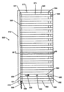
at one end as in FIGS. 2A-2E. As is shown, the first power bus 408 is
connected to the first
segments 422 at approximately the midpoint of the first segments, while the
second power bus
410 is connected to the second segments 422 at approximately the midpoint of
the second
segments. Thus, by coupling to the first and the second segments 420, 422 at
approximately
their midpoints, the first and the second power buses 408, 410 create multiple
parallel
connections and current paths through separate portions of the first and the
second segments
between the power buses.
[00881 In the embodiment shown in FIGS. 4A-4E, the first segments 420 of the
heating elements
404 are each formed from a strip of an electrically resistive thin film
attached to the first surface
412 of the substrate 402 and adapted to emit infrared radiation in response to
a current flow. For
example, in some cases the first segments 420 are formed from a carbon-based
thin film, such as
is described with respect to FIGS. 2A-2E. In this embodiment the second
segments 422 are each
formed from a strip of an electrically conductive material (e.g., a metal)
attached to the second
surface 414 of the substrate 402 opposite and parallel to a corresponding
first segment 420.
Other materials, including printed and/or resistive materials are also
contemplated for the second
segments 422.
[00891 Referring to FIG. 4E, the second segments 422 are shown in dashed
lines, indicating they
are placed on the second surface 414 or other side of the substrate 402 from
the first segments
420. FIG. 4E schematically illustrates the first segments 420 as being
slightly wider than the
second segments 422 to allow discernment of the different segments in the
views. In some
embodiments, though, the first and the second segments 420, 422 are formed
with consistently
identical, or substantially identical, widths and are placed on opposite
surfaces of the substrate in
an overlapping, parallel configuration.
[00901 The first and the second segments 420, 422 are electrically coupled
together at both ends
of the segments. In some cases the segments may be coupled together through
the substrate 402
with a connection made through a void (not shown), as discussed with respect
to FIG. 2G. In
some cases the segments may instead be coupled together about the edges of the
substrate (not
shown), such as with a conductive foil strip or band, in a similar manner to
the configuration
described with respect to FIG. 2H.
CA 02729500 2011-01-26
-22-
[00911 In the example shown in FIGS. 4A-4F, the power buses 408, 410 extend
transverse to the
segments between the end connections of the first and the second segments.
Referring again to
FIG. 4A , the first power bus 408 extends across (e.g., underneath) and
electrically couples to the
first segments 420 at approximately the midpoint of the segments 420 (other
points of connection
are also contemplated). As shown in FIG. 4D, the second power bus 410 extends
across and
electrically couples to the second segments 422 at approximately the midpoint
of the segments
422. The first and the second power buses 408, 410 can be coupled to the first
segments 420 and
the second segments 422 of the heating elements 404 in any suitable manner.
Turning to FIGS.
4C and 4F, in some cases the power buses and the heating element segments are
sandwiched
together about the substrate 402 in a laminating process. For example, as
shown in FIG. 4C, the
first power bus 408 is placed (e.g., deposited, formed, attached, etc.) on the
first surface 412 of
the substrate 402, and the second power bus 410 is placed on the second
surface 414 of the
substrate 402. The first segment 420 of electrically resistive material is
then formed over top of
the first surface 412 of the substrate as well as over top of the first power
bus 408, providing a
secure and reliable coupling between the first power bus and the first
segment. A similar
procedure can be used to attach the second segment 422 to the substrate's
second surface 414
and the second power bus 410.
[00921 Thus, the panel 400 is formed as a laminate having multiple layers
proximate to the
electrical connections between the heating element and the power buses.
Specifically, in the
illustrated embodiment the laminate includes in order from top down shown in
FIG. 4C, the first
segment 420, the first power bus 408, the substrate 402, the second power bus
410, and the
second segment 422. Of course other layers may also be present in between or
outside of the
illustrated stack. For example, in some cases an outer insulative layer may be
placed adjacent
the first segment 420 and also adjacent the second segment 422 to electrically
insulate the entire
panel 200.
[00931 Referring to FIGS. 4A-4D, when a particular heating element 404 is
energized, a first
current 430 flows through a first portion 440 of the first segment and a first
portion 442 of the
second segment between a first connection point 431 at the first power bus 408
to a second
connection point 433 at the second power bus 410. As the first current 430
flows through the
first portion 440 of the first segment 420, it flows in a first direction 432
relative to the substrate
CA 02729500 2011-01-26
- 23 -
402 that is opposite a second direction 434 that it flows in the first portion
442 of the second
segment 422. In addition, a second current 450 flows through a second portion
452 of the first
segment and a second portion 454 of the second segment between the first
connection point 431
and the second connection point 433. As the second current 450 flows through
the second
portion 452 of the first segment 420, it flows in a first direction 462
relative to the substrate 402
that is opposite a second direction 464 that it flows in the second portion
454 of the second
segment 422. Because the same first current 430 flows through both first
portions of the first and
second segments, and the same second current 450 flows through both second
portions of the
first and the second segments, the opposite polarity EM fields that are
generated by the portions
of the segments have the same or substantially the same magnitudes, leading to
improved field
canceling and low frequency EM field reduction.
[0094] FIG. 5A is a side surface view of an infrared heating panel 500
according to an
embodiment of the invention. FIG. 5B is an end view of the infrared heating
panel 500 from
along line 5B-5B, and FIG. 5C is an enlarged end view of portion 5C shown in
FIG. 5B. FIG.
5D is an enlarged view of portion 5D shown in FIG. 5B. In general, the heating
panel 500
generates infrared radiation from electrical power, and is useful for
generating heat such as in the
infrared sauna 100 shown in FIG. 1. The heating panel 500 is similar in many
respects to the
heating panel 200 discussed with respect to FIGS. 2A-2E, and portions of that
discussion are also
applicable to the embodiment shown in FIGS. 5A-5F.
[0095] The heating panel 500 includes a substrate 502 that carries multiple
heating elements 504
positioned in a row across the panel. Each heating element 504 includes a
first segment 520
attached to a first surface 512 of the substrate and a second segment 522
attached to a second
surface 514 of the substrate 502. The first and second segments 520, 522 are
electrically
connected together in series at one end of the segments, in this embodiment
about an edge of the
substrate 502. The segments are electrically coupled to power conductors 506
via a first power
bus 508 and a second power bus 510. Similar to the embodiment in FIGS. 2A-2E,
the power
buses 508, 510 extend across opposite surfaces of the substrate 502 in a
parallel configuration at
one end of the heating elements.
CA 02729500 2011-01-26
-24-
[0096] The second segment 522 is attached to the substrate's second surface
514 opposite the
substrate from and parallel to the first segment 520 on the substrate's first
surface 512, in order
to provide an EM field reducing/canceling configuration. In a preferred
embodiment, the widths
of the first and the second segments are substantially equal, and the segments
are attached
opposite each other on the substrate such that both segments are centered on
and extend along a
plane perpendicular to the substrate. FIG. 5F shows the first segment 520 and
the second
segment 522 of a single heating element 504 in cross-section. As shown, the
first and the second
segments are attached opposite each other on the substrate 502 such that
corresponding first
edges 570, 572 of the segments are substantially aligned and corresponding
second edges 571,
573 are substantially aligned. This arrangement can provide a high degree of
low EM field
cancellation, though it is not strictly required.
[0097] As in the embodiment shown in FIGS. 2A-2E, when a particular heating
element 504 is
energized, a current 530 flows through the heating element 504 between a first
connection point
531 at the first power bus 508 to a second connection point 533 at the second
power bus 510. As
the current 530 flows through the first segment 520, it flows in a first
direction 532 relative to the
substrate 502 that is opposite a second direction that it flows in the second
segment 522.
Because the same current 530 flows through both the first segment 520 and the
second segment
522 of a particular heating element 504, the opposite polarity EM fields that
are generated by the
segments have the same or substantially the same magnitudes, leading to
improved field
canceling and low frequency EM field reduction.
[0098] As in the embodiment in FIGS. 2A-2E, the first power bus 508 extends
across and is
attached to the first surface 512 of the substrate to electrically connect
each of the first segments
520 of the heating elements 504 to the panel's power conductors 506. The
second power bus
510 (electrically coupled to each of the second segments 522 of the heating
elements) is attached
to the second surface 514 of the substrate 502, opposite from and in a
parallel arrangement with
the first power bus 508. The first and the second power buses 508, 510 may be
formed from any
suitable electrically conductive material, such as a metal (e.g., copper or
another other metal or
alloy). In the illustrated embodiment, the first and the second power buses
508, 510 are each
formed from a flat metal strip that is secured to the substrate 502 during a
laminating process
similar to construction of a printed circuit board. As shown, in some cases
the power buses are
CA 02729500 2011-01-26
-25-
placed adjacent to the surfaces of the substrate and pressed into the
substrate, flush with the
substrate surfaces 512, 514 as part of the laminating process. Of course,
metal strips may be
attached in other ways, including for example, with an adhesive, welding, or
another mechanism.
In certain embodiments the first and/or the second power buses may
alternatively be formed with
a different process such as screen printing, etching, deposition, or another
type of formation
methods.
[00991 The placement of the first power bus 508 and the second power bus 510
between the
power conductors 506 and the heating elements 504 set up currents of opposite
polarity within
the first and the second power buses. According to some embodiments of the
invention, the first
and the second power buses 508, 510 are preferably configured to reduce the
magnitude of
unwanted low frequency EM fields emanating from the heating panel 500. The
inventors have
found that in some cases the configuration of the first and the second power
buses has an
increased effect upon the magnitude of certain low frequency EM radiation when
compared with
the effect caused by individual heating elements 504. It is believed that
relatively high levels of
current flowing through the power buses in comparison to the current levels in
each heating
element 504 contribute to this effect.
[001001 In certain embodiments, the second power bus 510 is attached to the
second surface 514
of the substrate opposite from and in a parallel arrangement with the first
power bus 508. For
example, in some cases the first power bus 508 and the second power bus 510
extend along a
common plane intersecting the power buses perpendicular to the substrate 502.
As shown in
FIG. 5C, in some cases the first and the second power buses can be considered
to be centered
along a common plane (not shown). In addition, in some cases the width of the
second bus 510
is substantially equal to the width of the first bus 508. In a preferred
embodiment the widths of
the first and the second power buses are substantially equal, and the buses
are attached opposite
each other on the substrate 502 such that corresponding first edges 516, 518
of the buses are
substantially aligned and corresponding second edges 517, 519 are
substantially aligned (as
shown by the dashed lines in FIG. 5C). FIGS. 6A-6D are simplified views of the
heating panel
500 without the heating elements 504, providing a cleaner view of the opposite
and parallel
arrangement of the power buses. This arrangement of the power buses can
provide a high degree
of low frequency EM field cancellation, though it is not strictly required in
all cases. For
CA 02729500 2011-01-26
-26-
example, it is contemplated that the first power bus and the second power bus
could potentially
be offset a small amount, or could have different widths and/or be offset from
an exact mirrored
placement upon opposing surfaces of the substrate depending upon the level of
EM field
cancellation desired.
[001011 According to some embodiments, the configuration of the connections
between the
heating elements and the first power bus and/or the second power bus can also
reduce the
magnitude of unwanted low frequency EM fields emanating from a heating panel.
In some cases
each connection between the first segments of the heating elements and the
first power bus is
substantially identical to and matched by each corresponding connection
between the second
segments and the second power bus. It is believed that substantially identical
or mirrored
connections can contribute to increased cancellation of unwanted low frequency
EM fields,
though substantial identity is not strictly required in all embodiments. For
example, one or more
imperfectly matched connections providing less than ideal cancellation may be
sufficient in some
cases based on tradeoffs in performance, cost, manufacturing tolerances, and
other such factors.
[001021 Referring to FIGS. 5A and 5C, the first segments 520 of the heating
elements extend
across the substrate 502 perpendicular to the first power bus 508 and connect
to the power bus
508 at one end (at the left end as illustrated in FIG. 5A). In this
embodiment, each of the first
segments 520 overlaps the entire width of the first power bus 508, extending
across the width to
end substantially flush with the first edge 516 of the bus. Extending the
first segments 520
across the entire width of the bus can provide a more uniform junction 531
across the width of
the bus. It is believed that this leads to more uniform and consistent current
densities in the first
power bus 508, which can be more easily matched by the configuration of the
second power bus
and heating element second segments on the second surface 514 of the
substrate. Referring to
FIG. 5C, in some cases each of the second segments 522 overlaps the entire
width of the second
power bus 510, extending across the width to end substantially flush with the
first edge 518 of
the second power bus.
[001031 As shown in FIGS. 5A-5F, in some cases the heating panel 500 is formed
as a laminate
stack of multiple layers at certain locations in the panel, including for
example the substrate 502,
the power buses 508, 510, and the heating element segments 520, 522. Other
layers may also be
CA 02729500 2011-01-26
-27-
present in between or exterior to the illustrated layers. For example, in some
cases a first outer
insulative layer may be placed adjacent the first segments 520 and a second
outer insulative layer
may be placed adjacent the second segments 522 to provide electrical
insulation for the entire
panel 500. In addition, the number of layers may vary depending upon the level
of integration of
the power buses and heating elements (e.g., a bus and one or more heating
segments may be a
single, integral layer, or may be separately combined together). Referring to
FIG. 5C, in certain
cases the panel 500 comprises a plurality of layers proximate the electrical
connection of each
first segment to the first power bus and each opposite and parallel second
segment to the second
power bus. The layers include, in order, the first segment 520, the first
power bus 508, the
substrate 502, the second power bus 510, and the second segment 522.
[00104] Preferably, the substrate 502 is constructed from an insulative
material that electrically
insulates the first power bus 508 from the second power bus 510 and the
heating element first
segments 520 from the heating element second segments 522. The substrate 502
also preferably
(but not necessarily) provides a sturdy base for mounting or attaching the
heating elements 504.
For example, the substrate may be formed from a fiberglass material, such as
an FR-4 sheet of
glass reinforced epoxy. In some cases one or more materials commonly used in
the
manufacturing of printed circuit boards may make up the substrate 502.
[00105] The first segment 520 of each heating element is formed from a strip
of an electrically
resistive (e.g., semi-conducting) material adapted to emit infrared radiation
in response to a
current flowing through the material. The first segments 520 of the heating
elements 504 are
each formed from a strip of an electrically resistive (e.g., semi-conducting)
thin film attached to
the first surface 512 of the substrate 502 and adapted to emit infrared
radiation in response to a
current flowing through the material. In this case the material is a carbon-
based thin film
including one of the materials described above with respect to the heating
panel 200 of FIGS.
2A-2E. Of course, the choice of resistive material and dimensions of the
resistive material strip
can vary depending upon the desired heat generation and performance
characteristics (e.g.,
resistivity of the material). A resistive thin film may be formed upon the
substrate in any
suitable manner, including by thin film deposition or etching. In certain
cases a thin integral
strip of resistive material may be placed upon the substrate. In the
illustrated embodiment, it is
contemplated that the first segments 520 are applied using a screen printing
process using a
CA 02729500 2011-01-26
-28-
carbon based ink (e.g., a colloidal graphite ink), examples of which are
provided above with
respect to FIGS. 2A-2E.
[001061 In the illustrated embodiment, each of the second segments 522 of the
heating elements
are formed from a strip of an electrically conductive material (e.g., a metal)
attached to the
second surface 514 of the substrate 502. However, the second segments 522 can
be formed from
a variety of materials. In certain embodiments the second segment 522 may
instead be formed
from a strip of electrically resistive material, such as the same material
used for the first segment
520.
[001071 In certain embodiments the second segments 522 are each formed from a
flat strip of an
electrically conductive material attached to the second surface 514 of the
substrate 502 opposite
and parallel to a corresponding first segment 520. As shown in FIGS. 5B-5F,
the conductive
material is provided in the form of a flat, metal strip, such as a strip of
copper or other suitable
metal pressed into and/or adhered to the second surface 514 of the substrate.
In certain
embodiments, though, the conductive material is a particulate material
deposited upon the
substrate. For example, a conductive material may be screen printed upon the
substrate to
provide the second segments. In this case the same or similar screen printing
patterns can be
used for the top and bottom surfaces of the substrate, therefore minimizing
manufacturing
complexity and variations. In addition, the second segments need not be a
purely conductive
material, but in some cases may instead be formed from a more resistive or
semi-conductive
material. In certain cases the second segments 522 may be formed from the same
resistive
material used to form the first segments 520, which can simplify material
requirements.
[001081 Accordingly, the composition and application of heating element
segments can vary.
Table 1 below provides a summary of four possible combinations of materials.
Segment Material Application
First Segment Electrically Resistive Material Printed
Second Segment Electrically Conductive Material Metal Strip
First Segment Electrically Resistive Material Printed
Second Segment Electrically Conductive Material Printed
First Segment Electrically Resistive Material Applied Strip
Second Segment Electrically Conductive Material Metal Strip
CA 02729500 2011-01-26
-29-
First Segment Electrically Resistive Material Printed
Second Segment Electrically Resistive Material Printed
Table I
Of course, other combinations of materials in addition to those listed above
are also possible.
[001091 Referring to the embodiment in FIGS. 5B-5C, the heating element second
segment 522
includes a thin, flat strip of copper that extends across the second surface
514 of the substrate
502. The second segment 522 is placed adjacent the second power bus 510, which
is also a thin
flat strip of copper extending across the second substrate surface 514
perpendicular to the second
segment 522. In this embodiment the second segment 522 and second power bus
510 are
separate components, placed adjacent one other and then held together with a
laminating process.
In certain embodiments, though, the second power bus 510 and some or all of
the second
segments 522 may be integrally formed in a single layer. For example, the
power bus and
segments may be stamped out of a single metal sheet. In another embodiment,
both the second
power bus 510 and the second segments 522 are printed upon the substrate in a
single, integral
layer using the same material. In these cases the heating panel would include
a number of layers,
including, in order, the first segment 520, the first power bus 508, the
substrate 502, and the
combined second power bus/second segment layer.
[001101 FIG. 5D is an enlarged cross-sectional view of the end of the infrared
heating panel 500
shown in FIGS. 5A-5C. As discussed above, in certain embodiments the first
segment and the
second segment of a given heating element are electrically connected in series
at one end of the
segments. As discussed above, the segments can be connected together in a
variety of manners,
including through the panel substrate or around an edge of the substrate. As
seen in FIGS. 5A
and 5D, in this embodiment a connecting strip 550 is folded about the edge of
the substrate 501
to connect the first segment 520 with the second segment 522. The connecting
strip is preferably
a flat metal (e.g., copper) strip with a width similar to the widths of the
first and second
segments, though other materials may be used. In the illustrated embodiment,
the connecting
strip 550 connects to the first segment at a junction 552, but is integral to
the second segment
522.
CA 02729500 2011-01-26
-30-
[001111 Turning to FIG. 5E, in some cases the connecting strip 550 maybe
separate from the
first and the second segments 520, 522. In this embodiment, the separate
connecting strip 550 is
folded about the edge of the substrate 502 opposite from the power buses 508,
510. The
connecting strip 550 makes contact with the heating element first segment 520
at a first junction
552, and with the second segment 522 at a second junction 554. In some cases
the connecting
strip 550 may be pressed into the substrate 502 and somewhat flush with the
substrate surfaces as
a result of making the panel 500 with a printed circuit board fabrication
process.
1001121 While the embodiments in FIGS. 5A-5F illustrates the use of a flat,
thin copper strip for
the heating element second segments 522, in certain embodiments the second
segments may
instead be formed from a conductive (or alternately semi-conductive)
particulate matter
deposited on the second surface 514 of the substrate over the second power bus
510 and the
connecting strip 550. For example, the second segments 522 may be applied
using a screen
printing process. The inventors have found that in some cases forming the
bus/segment junction
533 and the connecting strip/segment junction 554 in this manner provides a
superior connection
between the components in terms of connection clarity and uniformity when
compared with
connections between adjacent metal strips. For example, when compressing
multiple layers of
metal strips together in a printed circuit board fabrication process, epoxy or
resin can squeeze in
between the metal strips, which contaminates the junction and leads to current
density
imperfections that can affect the level of EM noise produced. In contrast,
depositing the
segments upon the substrate and power buses/connecting strips using a screen
printing process
can provide a substantially uniform interface and uniform current densities.
[001131 As discussed above, the inventors have found that in some cases the
configuration of
the first and the second power buses has an increased effect upon the
magnitude of certain low
frequency EM radiation when compared with the effect caused by individual
heating elements
504. According to some embodiments of the invention, the first and the second
power buses
508, 510 are preferably configured to reduce the magnitude of unwanted low
frequency EM
fields emanating from the heating panel 500.
[001141 In certain embodiments the connections between the first and the
second power buses
508, 510 and the power conductors 506 are configured to reduce undesirable low
frequency EM
CA 02729500 2011-01-26
-31-
radiation generated by the connections. Turning to FIGS. 5A and 5E, in the
illustrated
embodiment a first power conductor 506A (e.g., a 120 VAC line) is electrically
connected to the
first power bus 508 at a first connection point 580. Similarly, a second power
conductor 506B
(e.g., a 0 VAC line) is electrically connected to the second power bus 510 at
a second connection
point 581. In some cases the second power conductor 506B may connect to the
second power
bus 510 through the substrate as illustrated in FIG. 5F, or may instead simply
connect from the
opposite, second surface 514 of the substrate. A soldered connection or any
other suitable
manner of connecting the power conductors can be used. As seen most clearly in
FIG. 5F, the
first and the second power buses extend out away from the nearest heating
element segments
520, 522 so that the connection points 580, 581 are removed some distance from
the heating
elements. The inventors have found that this configuration promotes more
uniform current
densities within the power buses, which may lead to more effective
cancellation of EM fields
generated by the power buses.
[001151 In testing an embodiment of the invention having a configuration
similar to that shown
in FIGS. 5A-5D and 5E, the inventors have found that certain measured low
frequency magnetic
field intensities are maintained at or below a 1.0 milligauss level at two
inches from the panel
across substantially the entire area of the heating elements 504. In further
testing, the inventors
found that certain low frequency field intensities are at or below a 1.2
milligauss level at two
inches from the panel across substantially the entire length and width of the
first and the second
power buses 508, 510, in addition to the solder connection points between the
power buses and
the power conductors 506. Thus this configuration can in some cases enable the
use of larger
manufacturing tolerance windows, especially with respect to the power buses,
making it easier to
produce acceptable products.
[001161 FIG. 7A is a side surface view of an infrared heating panel 700
according to another
embodiment of the invention. FIG. 7B is a cross-sectional view of the infrared
heating panel 700
of FIG. 7A along line 7B-7B. FIG. 7C is an enlarged view of one end of the
infrared heating
panel 700 shown in FIG. 7B. FIG. 7D is an enlarged view of another end of the
infrared heating
panel 700 shown in FIG. 7B. FIG. 7E is an enlarged side end view of a
connection portion of the
infrared heating panel 700 of FIG. 7A. The heating panel 700 is similar in
many respects to the
CA 02729500 2011-01-26
-32-
heating panel 500 discussed with respect to FIGS. 5A-5F, and portions of that
discussion are also
applicable to the embodiment shown in FIGS. 7A-7E.
1001171 The heating panel 700 includes a substrate 702 that carries multiple
heating elements
704 positioned in a row across the panel. Each heating element 704 includes a
first segment 720
attached to a first surface 712 of the substrate and a second segment 722
attached to a second
surface 714 of the substrate 702. The first and second segments 720, 722 are
electrically
connected together in series at one end of the segments, in this embodiment
about an edge of the
substrate 702. The segments are electrically coupled to power conductors 706
via a first power
bus 708 and a second power bus 710.
[001181 Similar to the embodiment in FIGS. 5A-5F, the power buses 708, 710
extend across
opposite surfaces of the substrate 702 in a parallel configuration at one end
of the heating
elements. The first power bus 708 extends across and is attached to the first
surface 712 of the
substrate. The second power bus 710 is attached to the second surface 714 of
the substrate 702,
opposite from and in a parallel arrangement with the first power bus 708. The
first and the
second power buses 508, 510 may be any suitable electrically conductive
material, such as those
described elsewhere herein, and can be attached to the substrate in any
suitable manner (e.g.,
printed or applied).
1001191 In the illustrated embodiment, each of the first and the second power
buses 708, 710 is
an elongated flat strip of material having opposing ends and opposing sides,
as well as multiple
integral tabs extending out along one of the sides. For example, with
reference to FIGS. 7A and
7C, the first power bus 708 includes opposing first and second ends 743, 745,
and opposing first
and second sides 747, 749. The first power bus 708 also includes multiple tabs
760 extending
out from the second side 749 of the bus, in the direction of the heating
elements 704. The
heating elements 704 extend across and are attached to the substrate in a
perpendicular
orientation to the power buses in a similar fashion to other embodiments
described herein. In
this embodiment, the first and the second segments 720, 722 of the heating
elements extend
across the first and second surfaces of the substrate toward the power buses,
but do not contact
the power bus main flat strip. Instead, each of the first segments 720
attaches to one of the tabs
CA 02729500 2011-01-26
- 33 -
760 extending out from the first power bus at junction 731, and each of the
second segments 722
attaches to one of the tabs 762 extending out from the second power bus at
junction 733.
[00120] Accordingly, each of the heating element segments' connection to
either the first or
second power bus is removed some distance from the main, elongated flat strip.
The inventors
have found that this configuration can lead to more effective cancellation of
certain EM fields
generated by the power buses. It is believed that this configuration promotes
more uniform
current densities within the power buses (thus leading to better low frequency
EM field
cancellation) because the joints between the heating element segments and the
power bus are
moved into an area transporting less current than in the main strip of the
buses (each joint being
along a single heating element).
[00121] The bus configuration including a main strip with several tabs
extending out from one
side can be formed in any suitable manner known in the art. In a preferred
embodiment, the
main strip and tabs are integrally formed, thus avoiding the need for further
connections between
components which can lead to increased low frequency EM field generation. It
is contemplated
that in certain embodiments a stamping process or water jet cutting process
could be used to
form the main bus line and tabs from a sheet of metal. The sheared edges of
the work piece
preferably present continuous, sharp edges with minimum point defects to
reduce the likelihood
of short circuits forming between the first and the second power buses. Of
course a wide variety
of manufacturing tolerances may be suitable for forming the edges depending
upon the thickness
and insulative properties of the substrate, among other factors.
[00122] FIG. 8A is a side surface view of an infrared heating panel 800
according to an
embodiment of the invention. FIG. 8B is a cross-sectional view of the infrared
heating panel 800
of FIG. 8A along line 8B-8B. FIG. 8C is an enlarged view of one end of the
infrared heating
panel 800 shown in FIG. 8B. FIG. 8D is an enlarged view of another end of the
infrared heating
panel 800 shown in FIG. 8B. FIG. 8E is an enlarged side end view of a
connection portion of the
infrared heating panel 800 of FIG. 8A. The heating panel 800 is similar in
many respects to the
heating panel 500 discussed with respect to FIGS. 5A-5F, and portions of that
discussion are also
applicable to the embodiment shown in FIGS. 8A-8E.
CA 02729500 2011-01-26
-34-
[00123] The heating panel 800 includes a substrate 802 that carries multiple
heating elements
804 positioned in a row across the panel. Each heating element 804 includes a
first segment 820
attached to a first surface 812 of the substrate and a second segment 822
attached to a second
surface 814 of the substrate 802. The first and second segments 820, 822 are
electrically
connected together in series at one end of the segments, in this embodiment
about an edge of the
substrate 802. The segments are electrically coupled to power conductors 806
via a first power
bus 808 and a second power bus 810.
[00124] Similar to the embodiment in FIGS. 5A-5F, the power buses 808, 810
extend across
opposite surfaces of the substrate 802 in a parallel configuration at one end
of the heating
elements. The first power bus 808 extends across and is attached to the first
surface 812 of the
substrate. The second power bus 810 is attached to the second surface 814 of
the substrate 802,
opposite from and in a parallel arrangement with the first power bus 808. The
first and the
second power buses 508, 510 may be any suitable electrically conductive
material, such as those
described elsewhere herein, and can be attached to the substrate in any
suitable manner (e.g.,
printed or applied).
[00125] In this embodiment, the first segment 820 of each heating element 804
extends across
the first surface 812 of the substrate 802 and is electrically connected to
the first power bus 808
at a first junction 831. Each of the first segments 820 preferably overlaps
the entire width of the
first power bus 808, extending across the width to end substantially flush
with the edge of the
bus, although this is not required. Each of the second segments 822 extend
across the second
surface 814 of the substrate toward, but do not contact the second power bus
810. Instead, the
heating panel 800 includes multiple bridging strips 890 that connect each of
the second segments
to the second power bus. Accordingly, the heating panel has a laminate form in
which near the
power buses, the laminate has a plurality of layers including, in order, the
first segment, the first
power bus, the substrate, the second power bus, and a bridging strip.
[00126] As discussed above, the composition and application of heating element
segments can
follow any of a variety of combinations of materials and methods of
attachment. In the
embodiment shown in FIGS. 8A-8E, the first segments 820 of the heating
elements are
CA 02729500 2011-01-26
-35-
preferably printed strips of an electrically resistive material (e.g., a
graphite ink). The second
segments 822 are preferably flat strips of a conductive metal, such as copper.
[00127] As discussed above, in some cases depositing a particulate resistive
material to create
the bus/segment junction 831 is thought to provide a superior connection
between the first power
bus and each of the first segments 820 in terms of connection clarity and
uniformity when
compared with connections between adjacent metal strips (see, e.g., the
junction 533 between the
second power bus 510 and the second segments 522 in FIG. 5C). In addition, in
cases where it is
desirable to use a printed electrically resistive material for the first
segments 820 and a metal
strip for the second segments 822, the current profile surrounding the
respective junctions with
the first and the second power buses will vary, thus tending to generate
undesirable low
frequency EM emissions due to the mismatch in current densities in the first
and the second
power buses.
[00128] The use of multiple bridging strips 890 to connect each of the second
segments 822 to
the second power bus 810 can help provide more uniform current profiles in the
first and second
power buses, which can also reduce undesirable EM emissions generated at the
bus-segment
junctions. The bridging strips 890 are preferably made from the same material
as the heating
element first segments 820, which is this case is a printed electrically
resistive material. As
shown in FIG. 8C, the bridging strip 890 connects to the second power bus 810
at a first junction
835 and to the second segment 822 at a second junction 837. Because the
bridging strip is
formed from the same material as the first segment 820, the first junction 835
tends to mirror the
behavior of the junction 831 between the first segment and the first power
bus, thus leading to
increased EM field cancellation at the bus where current levels tend to be
higher than in each
individual heating element.
[00129] In the illustrated embodiment, each of the bridging strips 890 extends
from the second
power bus 810 and ends in the junction 837 at the second segment of each
heating element.
Although not shown, in some cases the bridging strips may extend further and
overlap a greater
portion of the second segments. In certain embodiments, the bridging strips
may extend across
the entire substrate between second power bus 810 and the connecting strip
850, thus entirely
CA 02729500 2011-09-09
-36-
overlapping the second segments 822. Other intermediate degrees of overlap are
also
contemplated.
[00130] Some embodiments of the invention provide methods for reducing
electromagnetic emissions in an infrared sauna. In some cases a method
includes providing one
of the infrared heating panels described above, mounting it in an infrared
sauna, and energizing
the panel to generate infrared radiation to warm a sauna user, while also
reducing, canceling, or
substantially canceling, certain low frequency and/or extremely low frequency
EM fields.
[00131] In another embodiment, a method for reducing electromagnetic emissions
in an
infrared sauna includes providing one or more infrared heating panels. Each
heating panel
includes an electrically insulative planar substrate and at least one infrared
heating element. The
heating element includes an elongated first segment attached to a first
surface of the substrate
and an elongated second segment attached to a second surface of the substrate.
The first and
second segments are electrically coupled together to provide a continuous
conduction path. The
method also includes producing a first current through the first segment of
the heating element to
generate infrared radiation for heating a human in the infrared sauna. The
first current flows
through the first segment in a first direction relative to the substrate, thus
generating a
corresponding first electromagnetic field at frequencies below the infrared
radiation. The
method also includes flowing the first current through the second segment of
the heating element
in a second direction relative to the substrate opposite the first direction
in order to generate a
corresponding second electromagnetic field that counteracts or cancels the
first electromagnetic
field.
[00132] Thus, embodiments of the invention are disclosed. Although the present
invention
has been described in considerable detail with reference to certain disclosed
embodiments, the
disclosed embodiments are presented for purposes of illustration and not
limitation and other
embodiments of the invention are possible.