Note: Descriptions are shown in the official language in which they were submitted.
CA 02729611 2010-09-13
WO 2009/114284 PCT/US2009/035338
SOLAR ENERGY PRODUCTION SYSTEM
Solar photovoltaic (PV) cells currently furnish power for remote sites on
earth and for
space vehicles, where other power sources are expensive or unavailable. Solar
PV
technologies cannot yet compete for most central site power generation
applications, because
they are all significantly more expensive than other available energy sources
(e.g. coal, gas,
and nuclear).
Yet solar PV technology remains of interest because the existing forms of
power
generation are certainly going to become more costly as their supplies
diminish. All forms of
solar power are also renewable and eoo-friendly. There is currently a push to
make solar PV
cells less costly and also to increase their efficiency (to convert solar
energy directly into
electricity).
The current global cost of electrical energy generation alone is roughly
$300M/hr; and
the overall "energy marketplace" is double that figure. Any energy production
capability that
can be installed at a lower cost than the current installation cost for coal
fired or nuclear
power will be warmly welcomed.
Current problems with solar PV cells are twofold. First, they cannot compete
with
traditional energy sources for central site power generation on the basis of
their installed cost
(roughly $7-$ 10/installed watt for solar versus $4-$5/watt for coal, nuclear,
or natural gas).
Second, solar PV cells currently require the same scarce semiconductor
materials that are
used in several numerous electronic industries (computers, LED, and diode
laser). In order to
make solar PV cells competitive as a source for electrical power generation,
they must have
much lower production costs, become significantly more efficient in their
conversion of solar
energy to electricity, and they must be made almost entirely of materials that
are cheap and
plentiful.
1
CA 02729611 2010-09-13
WO 2009/114284 PCT/US2009/035338
Current solar cell technology employs single junction cells for rooftop
applications.
Such cells typically are about 12% to 18% efficient and require purified
silicon - which is in
high demand by the electronics industry for other applications. In order to
increase solar cell
efficiency, numerous attempts have been made to build "multi junction" cells.
These stacked
cells are designed such that the different layers of the cell absorb different
energy bands of
the incident solar energy.
Such multi-junction cells have been demonstrated to be more efficient - the
best
examples achieving efficiencies just in excess of 40% in the laboratory.
However, the
complexity restricts the materials (such as Ge, IL[-V) that must be used in
their assembly and
they are currently much more expensive than the single junction cells.
In the current manufacture of concentrating solar cells, maximum efficiencies
of 40%
or more can be achieved (Spectrolab, Boeing), but only if the thickness of
each cell layer,
including coatings, can be vapor deposited with great precision. The thickness
of each cell
layer must be precisely controlled to maintain the same electrical current
production in every
part of the cell. This is especially true for nlulti-junction cells, where
equal currents between
junctions require expensive, precision tunnel diodes between each junction. In
addition to
higher processing costs associated with precision manufacturing, these multi
juunction
components must also be "lattice matched" with each other.
This means the cell designer is restricted to scarce, expensive, semiconductor
alloy
combinations in order to achieve precisely the same molecular lattice spacing
at each
junction.
To compete in the central site power generation marketplace, solar PV cells
and
concentrating systems must cost less than $2/installed Watt. Also, they must
attain high
efficiencies in order to make them "duty cycle" competitive. A typical central
site power
2
CA 02729611 2010-09-13
WO 2009/114284 PCT/US2009/035338
generation facility currently is "on station" for --- 20 hr/day. In the
southwestern US,
stationary, SOA solar panels produce electricity for only about 6 hours/day
for a "duty cycle"
of - 25%. A solar cell that tracks the sun will produce electricity for an
average of about 11
hours a day.
SUMMARY OF THE INVENTION
A device in accordance with the present invention for generating solar
photovoltaic
energy generally includes an optic for focusing the solar radiation, followed
by a collimating
optic, a semiconductor optical gate wedge disposed for dispersing incident
solar radiation into
a plurality of adjacent wavelength bands. The wedge may include multiple
coatings in order
to reduce reflection losses.
An array of photovoltaic cells is provided with each cell formed from material
for
absorbing and converting a corresponding wavelength band, dispersed by the
wedge, into
electrical energy. A refracting optic is disposed between the wedge and the
array for
directing separated wavelength bands onto corresponding photovoltaic cells.
In this manner, each semi-conducting material in a cell in the dispersed array
is
disposed to only the wavelength range from the incident solar spectrum that
matches the
materials ability to absorb and convert sunlight into electricity.
These "unstacked" solar cell arrays can be built with much lower processing
costs
using plentiful and less expensive materials than existing multi junction
cells. The resulting
photovoltaic (PV) cell array electrical/total power fraction (efficiency) will
exceed 40% once
each PV material and cell has been optimized for its appropriate photon
wavelength or energy
In contrast, as hereinabove noted, the state of the art solar panel systems
are restricted
to an overall efficiency of 18% or less,
3
CA 02729611 2010-09-13
WO 2009/114284 PCT/US2009/035338
More particularly, a refracting optic is disposed between the wedge and the
cell array
for the purpose of directing separated wavelength bands onto corresponding
photovoltaic
cells. Each cell comprises a single junction, either IH-V or Si, photovoltaic
cell which
significantly reduces the cost of the device.
More specifically, as an example, the array may include five cells with the
first cell
absorbing solar photons of energy between 0.95 and 1.15 eV, the second cell
absorbing solar
photons of energy between 1.2 and 1.4 eV, the third cell absorbing solar
photons of energy
between 1.45 and 1.7 eV, the fourth cell absorbing solar photons of energy
between 1.75 and
2.1 eV, and the fifth cell absorbing solar photons of energy between 2.15 and
2.8 eV.
Still more particularly, the first cell may be formed from GaInAsP the second
cell
may be formed from Si, the third cell may be formed from GaAs, the fourth cell
may be
formed from GaTnP and the fifth cell may be formed from Al2GaInP4.
To further increase the efficiency and effectiveness of the device, the
refracting optic
may be disposed for spatially dispersing light from the wedge onto the
photovoltaic cells
incident perpendicular to the cell surfaces.
A method in accordance with the present invention provides for optimization of
a
photovoltaic cell array, and generally includes focusing solar radiation onto
a semi-conductor
optical gate wedge, dispersing the solar radiation by way of the gate wedge
into a plurality of
adjacent wavelength bands, and directing the adjacent wavelengths bands such
that they are
incident perpendicular to the surfaces of the a photovoltaic cell array. More
particularly, the
method further includes arranging a plurality of single junction, either ffl-V
or Si,
photovoltaic cells which form a linear array.
4
CA 02729611 2010-09-13
WO 2009/114284 PCT/US2009/035338
BRIEF DESCRIPTION OF THE DRAWINGS
The present invention may be more readily understood by consideration of the
following detailed description when taken in conjunction with the accompanying
drawings, in
which:
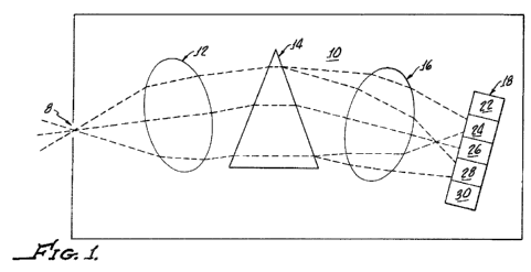
Figure 1 is a representation of the photovoltaic (PV) box in accordance with
the
present invention for generating solar photovoltaic energy which generally
shows a
collimation optic, a semi-conductor optical gate wedge, an array of
photovoltaic cells, and an
array optic disposed between the wedge and the array;
Figure 2 is a representation of the solar energy production system, including
a
focusing optic disposed in an operative relationship with the PV box
illustrated in Figure 1;
Figure 3 is a representation of one embodiment of the focusing optic shown in
Figure
2 in accordance with the present invention illustrating a Fresnel array with
four mirrors;
Figure 4 is a representative of an alternative embodiment of the focusing
optic shown
in Figure 2 in accordance with the present invention illustrating a thirty-six
mirror Fresnel
array; and
Figure 5 is a plot of electrical watts generated versus the solar spectrum as
a function
of photon energy in eV illustrating the efficiency of the device in accordance
with the present
invention through the use of an array of single junction diode photovoltaic
cells.
DETAILED DESCRIPTION
With reference to Figure 1, there is represented a photovoltaic (PV) box 10 in
accordance with the present invention for generating solar photovoltaic energy
which
5
CA 02729611 2010-09-13
WO 2009/114284 PCT/US2009/035338
The Fresnel lens used for the focusing optic 4 and the refracting optics 16
are
available from Edmunds Optics or Opto Sigma, or Newport Optical. The
semiconductor
optical gate wedges 14, as described in the hereinabove referenced U.S.
Patents are available
through TWO-SIX and Janos Optical,
A conventional solar tracker (not shown) may be utilized in order to cause the
focusing optic 4a, 4b to be normal to incoming solar radiation within 0.1
degree.
Importantly, the arrangement of the present invention enables a linear array
of
photovoltaic cells which can comprise a single junction, either IH-V or Si
photovoltaic cells.
Any number of suitable photovoltaic cells 22-30 may be utilized in the array,
while five are
shown, any number, for example three, may be utilized depending upon the size
of the solar
energy production system 2. These "unstacked" solar cell arrays 18 have much
lower
processing costs using plentiful and less expensive materials. The
photovoltaic cell array 18
may have an efficiency exceeding 40% since each photovoltaic material and cell
is optimized
for its appropriate photon wavelength or energy incident due to the wedges. In
turn., the
wedges 14 have refractive indices that are approximately the same as the
surface of
photovoltaic cell array 18 which are connected in series to increase voltage.
In addition,
these PV cells are preferably impedance snatched with one another by external
electrical
connections in order to maximize the total electrical output.
With an array of five cells, a first cell 22 may be constructed for absorbing
solar
photons of energy between 0.95 and 1,15 eV, the second cell 24 may be
constructed for
absorbing photons of energy between 1.20 and 1.4 eV, the third cell 26 may be
constructed
for absorbing solar photons of energy between 1.45 and 1.7 eV, a fourth cell
28 may be
constructed for absorbing solar photons of energy between 1.75 and 2.1 eV, and
the fifth cell
may be constructed for absorbing solar photons of energy between 2.15 and 2.18
eV.
7
CA 02729611 2010-09-13
WO 2009/114284 PCT/US2009/035338
generally includes a collimating optic 12, a semiconductor optical gate wedge
14 which may
be coated if desired to selectively reflect incident radiation, a refracting
optic 16 disposed
between the wedge 14 and an array 18 of photovoltaic cells 22, 24, 26, 28, 30.
The solar
radiation enters the PV box 10 through the window opening S.
As represented in Figure 2, the solar energy production system 2 consists of
the
focusing optic 4 which focuses solar radiation on the window opening 8 to the
PV box 10.
The PV box is attached to the support for the focusing optic 4 with several
struts 6.
The focusing optic 4 may be of any suitable configuration and size as
represented, for
example, in Figure 3 wherein focusing optic comprises a Fresnel array 4a of
four mirrors 34,
36, 38, 40 each having a diameter of 0.5 in, which are spaced apart from two
semiconductor
optical gate wedges 14 at a distance of about 0.5 m. The wedges 14 have an
area of about
0.04 m2. Given solar input of 920 Whn2 and a focusing optic collecting area of
0.78 m2, the
power at the wedges is about 722 W. With 40% efficiency, the power output
would be
almost 300 watts of electrical power. Suitable wedges 14 are described in U.S.
Patent Nos.
7,238,954 and 7,286,582 to Fay. These references are incorporated herewith in
their entirety
for the purpose of describing suitable wedges 14 for use in the present
invention.
The PV box 10 may be scaled to any suitable size by increasing the size of the
focusing optic 4, collimating optic 12, wedges 14, refracting optics 16, and
the photovoltaic
cell array 18. For example, as illustrated in Figure 4, the focusing optic 4b
may include an
array of thirty-six mirrors arranged in three circles with a total diameter of
l4m and a
collecting area of 113 m2. Given solar input of 920 W/m2 and a focusing optic
collecting area
of 113 m2, the power at the wedges is about 105,000 W. With 40% efficiency,
the power
output would be almost 42,000 watts of electrical power. In this instance,
nine wedges 14
may be utilized having an area of 0.18 m2. The amount of solar energy
collected utilizing the
focusing optics 4a and 4b represent embodiments suitable for home and
commercial power
production respectively.
6
CA 02729611 2010-09-13
WO 2009/114284 PCT/US2009/035338
More specifically, the cell 22 may be GaInAsP, the second cell 24 may be Si.,
the third
cell 26 may be GaAs, the fourth cell 28 may be GaInP2, and the fifth cell 30
may be
A12GaInP4. These cells are based on well established light emitting diode, or
LED, industry
technology. These LEDs convert electrical current into light of a plurality of
wavelengths,
each near the band gap of the material. These same LEDS can (with small design
modifications) receive sunlight within each wavelength band dispersed by the
wedge and
convert it into electrical current with high efficiency.
Such LED based photovoltaic cells are available from a number of manufacturers
such as, for example, Cree, Inc. However, suitable materials are not limited
to those
hereinabove recited, but may include materials .from class IV, III-V, or 11-VI
material types
which are utilized to optimize the photovoltaic conversion of the near
infrared invisible
regions of the solar spectrum to electricity. Further description of materials
suitable for use in
the present invention is described in U.S. 5,617,206, 7,238,954, and 7,286,582
to Fay. These
references are also incorporated herewith by this specific reference thereto.
As hereinabove noted, the efficiency of the photovoltaic cells 22-30 is
provided by the
optical gate wedge 18 which causes dispersion sufficient to overcome the
limitation imposed
by the optics of the angular diameter of the sun (9.3 milli-radians). The
refracting optic 16
completes the dispersion and focusing of the light from different wavelengths
(photon
energy) to the different cells 22-30. The refracting optic 16 further
spatially disperses the
light perpendicularly to the cells 22-30, in order to prevent overheating of
the photovoltaic
array 18 cells 22-3 0.
The efficiency of the device is illustrated in Figure 5. The solar spectrum
above the
atmosphere (described in the Fig.5 caption as AMO, or at air mass zero) is
illustrated as curve
52 and the watts of electricity produced illustrated as curve 54 across the
solar spectrum with
the range of solar conversion of each cell indicated by the panels 1, 2, 3, 4,
5 corresponding to
the cells 22, 24, 26, 28, 30.
8
CA 02729611 2010-09-13
WO 2009/114284 PCT/US2009/035338
Although there has been hereinabove described a specific solar energy
production
system and method in accordance with the present invention for the purpose of
illustrating the
manner in which the invention may be used to advantage, it should be
appreciated that the
invention is not limited thereto. That is, the present invention may suitably
comprise, consist
of, or consist essentially of the recited elements. Further, the invention
illustratively
disclosed herein suitably may be practiced in. the absence of any element
which is not
specifically disclosed herein. Accordingly, any and all modifications,
variations or equivalent
arrangements which may occur to those skilled in the art, should be considered
to be within
the scope of the present invention as defined in the appended claims.
9