Note: Descriptions are shown in the official language in which they were submitted.
CA 02730296 2014-09-02
,
1 METHOD AND APPARATUS FOR CURING THIN FILMS ON LOW-
2 TEMPERATURE SUBSTRATES AT HIGH SPEEDS
3
4 BACKGROUND OF THE INVENTION
6 1. Technical Field
7
8 The present invention relates to curing systems in general, and, in
particular, to a
9 method for curing thin films on substrates at low temperatures.
11 2. Description of Related Art
12
13 Printed electronics is the convergence of the semiconductor industry
and the
14 printing industry. The notion of printing electronic circuits instead of
printing reading
materials is seductive to printers as they can see the potential for doing
"high value" print
16 jobs without making major changes to their equipment. Similarly,
electronic circuit
17 manufacturers view the notion of printing electronic circuits as equally
seductive because
18 it allows them to fabricate electronic circuits in large volumes at a
relatively low cost.
19
During the manufacturing of electronic circuits, most thin film coatings need
to be
21 thermally processed, and the effectiveness of most thermal curing
processes is related to
22 the product of temperature and time. For example, the typical approach
to curing a thin
23 film is placing the thin film in an oven set to the maximum working
temperature of a
- 1 -
CA 02730296 2011-01-10
WO 2010/005609
PCT/US2009/039174
1 substrate on which the thin film is disposed, and allowing the thin film
to be cured within
2 some reasonable amount of time.
3
4 Since printed electronic circuits are typically associated
with high volume
and low cost, the substrates for the printed electronic circuits need to be
made of relatively
6 cheap materials such as paper or polymer instead of traditional substrate
materials such as
7 silicon, quartz, glass, ceramic, FR4, etc. However, paper or polymer has
a much lower
8 temperature of decomposition than silicon, quartz, glass, ceramic, FR4,
etc., and the much
9 lower temperature necessitates a longer cure time for thin films. For
example, the
lo maximum working temperature of polyethylene terephthalate (PET) is 150
C, and a typical
11 curing time for a silver based conductive film at this temperature is in
the order of minutes.
12 Such a long curing time makes the proposition of printing electronic
circuits on paper on
13 polymer much less economically attractive.
14
Consequently, it would be desirable to provide a method and apparatus for
16 thermally processing thin films on low-temperature substrates at a
relatively high speed.
- 2 -
CA 02730296 2016-09-19
1 SUMMARY OF THE INVENTION
2
3 Certain exemplary embodiments can provide a curing apparatus comprising:
a
4 conveyor system for transporting a layer of thin film mounted on a low-
temperature
substrate; a strobe head having a flash lamp for providing a plurality of
electromagnetic
6 pulses to said layer of thin film; a strobe control module for
controlling power, duration
7 and repetition rate of said plurality of electromagnetic pulses generated
by said flash
8 lamp; a conveyor control module, in conjunction with said strobe control
module, for
9 synchronizing in real-time said repetition rate of said plurality of
electromagnetic pulses
with the speed at which said low-temperature substrate is being moved past
said strobe
11 head; and means for blowing air to cool said thin film after said thin
film has been
12 exposed to one of said electromagnetic pulses.
13
14 Certain exemplary embodiments can provide a curing apparatus comprising:
a strobe
head having a flash lamp for providing a plurality of electromagnetic pulses
to a layer
16 of thin film mounted on a low-temperature substrate; a strobe control
module for
17 controlling power, duration and repetition rate of said plurality of
electromagnetic
18 pulses generated by said flash lamp; means for moving said low-
temperature substrate
19 past said strobe head; a control module for providing real-time
synchronization of said
repetition rate of said plurality of electromagnetic pulses with a speed at
which said
21 low-temperature substrate is being moved past said strobe head; and
means for blowing
22 air to cool said thin film after said thin film has been exposed to one
of said
23 electromagnetic pulses.
24
Certain exemplary embodiments can provide a curing apparatus comprising: a
conveyor
26 system for transporting a layer of thin film mounted on a low-
temperature substrate; a
27 strobe head having a flash lamp for providing a plurality of
electromagnetic pulses to said
28 layer of thin film; a strobe control module for controlling power,
duration and repetition
29 rate of said plurality of electromagnetic pulses generated by said flash
lamp; a conveyor
- 3 -
CA 02730296 2016-09-19
1 control module, in conjunction with said strobe control module, for
synchronizing in real-
2 time said repetition rate of said plurality of electromagnetic pulses
with the speed at
3 which said low-temperature substrate is being moved past said strobe
head; and means
4 for cooling said thin film by removing heat from said substrate via
conduction after said
thin film has been exposed to one of said electromagnetic pulses.
6
7 Certain exemplary embodiments can provide a curing apparatus comprising: a
strobe
8 head having a flash lamp for providing a plurality of electromagnetic
pulses to a layer of
9 thin film mounted on a low-temperature substrate; a strobe control module
for controlling
power, duration and repetition rate of said plurality of electromagnetic
pulses generated
11 by said flash lamp; means for moving said low-temperature substrate past
said strobe
12 head; a control module for providing real-time synchronization of said
repetition rate of
13 said plurality of electromagnetic pulses with a speed at which said low-
temperature
14 substrate is being moved past said strobe head; and means for cooling
said thin film by
removing heat from said substrate via conduction after said thin film has been
exposed to
16 one of said electromagnetic pulses.
17
18 All features and advantages of the present invention will become
apparent in the
19 following detailed written description.
- 3a -
CA 02730296 2011-01-10
WO 2010/005609
PCT/US2009/039174
1 BRIEF DESCRIPTION OF THE DRAWINGS
2
3 The invention itself, as well as a preferred mode of use,
further objects, and
4 advantages thereof, will best be understood by reference to the following
detailed
description of an illustrative embodiment when read in conjunction with the
accompanying
6 drawings, wherein:
7
8 Figure 1 is a diagram of a curing apparatus, in accordance
with a preferred
9 embodiment of the present invention;
11 Figure 2 is a diagram of a thermal barrier layer on a low-
temperature
12 substrate, in accordance with a preferred embodiment of the present
invention;
13
14 Figure 3 is a diagram of an air knife within the curing
apparatus from Figure
1, in accordance with a preferred embodiment of the present invention; and
16
17 Figure 4 is a diagram of a cooling roller within the curing
apparatus from
18 Figure 1, in accordance with a preferred embodiment of the present
invention.
- 4 -
CA 02730296 2011-01-10
WO 2010/005609
PCT/US2009/039174
1 DETAILED DESCRIPTION OF A PREFERRED EMBODIMENT
2
3
For the present invention, curing is defined as thermal processing, which
4
includes drying (driving off solvent), particle sintering, densification,
chemical reaction
initiation, phase transformation, grain growth, annealing, heat treating, etc.
When curing
6
materials on a low-temperature substrate, such as polymer or paper, one
limiting factor in
7
attaining a good cure is the decomposition of the substrate because a thin
film (which is
8
defined as a layer of material of less than 100 microns thick) often needs to
be processed
9
at temperatures close to or even beyond the decomposition temperature of the
substrate.
Furthermore, even if the thin films can be cured at a low temperature, the low
11
decomposition temperature of the substrate increases the amount of time to
thermally cure
12
the material on the substrate. The above-mentioned problems can be overcome by
the
13 curing apparatus of the present invention.
14
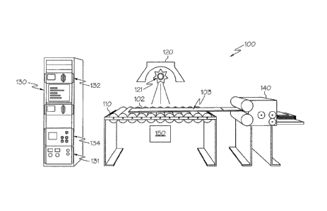
Referring now to the drawings and in particular to Figure 1, there is depicted
16 a
diagram of a curing apparatus, in accordance with a preferred embodiment of
the present
17
invention. As shown, a curing apparatus 100 includes a conveyor belt system
110, a strobe
18
head 120, a relay rack 130 and a reel-to-reel feeding system 140. Curing
apparatus 100
19
is capable of curing a thin film 102 mounted on a low-temperature substrate
103 situated
on a web or individual sheets being moved across a conveyor belt at a
relatively high
21
speed. Conveyer belt system 110 can operate at speeds from 2 to 1000 ft/min,
for example,
22
to move substrate 103. Curing apparatus 100 can accommodate a web of any width
in
23 6-
inch increments. Thin film 102 can be added on substrate 103 by one or
combinations
24
of existing technologies such as screen printing, inkjet printing, gravure,
laser printing,
xerography, pad printing, painting, dip-pen, syringe, airbrush, flexographic,
chemical vapor
26 deposition (CVD), PECVD, evaporation, sputtering, etc.
27
28
Strobe head 120, which is preferably water cooled, includes a high-intensity
29
pulsed xenon flash lamp 121 for curing thin film 102 located on substrate 103.
Pulsed
xenon flash lamp 121 can provide light pulses of different intensity, pulse
length and pulse
- 5 -
CA 02730296 2011-01-10
WO 2010/005609
PCT/US2009/039174
1 repetition frequency. For example, pulsed xenon flash lamp 121 can
provide 10 As to 10
2 ms pulses with a 3" by 6" wide beam pattern at a pulse repetition rate of
up to 1 kHz. The
3 spectral content of the emissions from pulsed xenon flash lamp 121 ranges
from 200 nm
4 to 2,500 nm. The spectrum can be adjusted by replacing the quartz lamp
with a cerium
doped quartz lamp to remove most of the emission below 350 nm. The quartz lamp
can
6 also be replaced with a sapphire lamp to extend the emission from
approximately 140 nm
7 to approximately 4,500 nm. Filters may also be added to remove other
portions of the
8 spectrum. Flash lamp 121 can also be a water wall flash lamp that is
sometimes referred
9 to as a Directed Plasma Arc (DPA) arc lamp.
11 Relay rack 130 includes an adjustable power supply 131, a
conveyor control
12 module 132, and a strobe control module 134. Adjustable power supply 131
can produce
13 pulses with an energy of up to 4 kiloJoules per pulse. Adjustable power
supply 131 is
14 connected to pulsed xenon flash lamp 121, and the intensity of the
emission from pulsed
xenon flash lamp 121 can be varied by controlling the amount of current
passing through
16 pulsed xenon flash lamp 121.
17
18 Adjustable power supply 131 controls the emission intensity of
pulsed xenon
19 flash lamp 121. The power, pulse duration and pulse repetition frequency
of the emission
from pulsed xenon flash lamp 121 are electronically adjusted and synchronized
to the web
21 speed to allow optimum curing of thin film 102 without damaging
substrate 103, depending
22 on the optical, thermal and geometric properties of thin film 102 and
substrate 103.
23
24 During curing operation, substrate 103 as well as thin film
102 are being
moved onto conveyor belt system 110. Conveyor belt system 110 moves thin film
102
26 under strobe head 120 where thin film 102 is cured by rapid pulses from
pulsed xenon flash
27 lamp 121. The power, duration and repetition rate of the emissions from
pulsed xenon
28 flash lamp 121 are controlled by strobe control module 134, and the
speed at which
29 substrate 103 is being moved past strobe head 120 is deteimined by
conveyor control
module 132.
- 6 -
CA 02730296 2011-01-10
WO 2010/005609
PCT/US2009/039174
1 A sensor 150, which can be a mechanical, electrical or optical
sensor, is
2 utilized to sense the speed of the conveyor belt of conveyor belt system
110. For example,
3 the conveyor belt speed of conveyor belt system 110 can be sensed by
detecting a signal
4 from a shaft encoder connected to a wheel that made contact with the
moving conveyor
belt. In turn, the pulse repetition rate can be synchronized with the conveyor
belt speed
6 of conveyor belt system 110 accordingly. The synchronization of the
strobe pulse rate f
7 is given by:
8 0.2 * S * 0
9 f ----------
11 where f= strobe pulse rate [Hz]
12 S = web speed [ft/min]
13 0 = overlap factor (i.e., the average number of strobe pulses
that are
14 received by the substrate)
W = curing head width [in]
16
17 For example, with a web speed of 200 ft/min, an overlap factor of 5, and
a curing head
18 width of 2.75 inches, the pulse rate of the strobe lamp is 72.7 Hz.
19
By combining a rapid pulse train with moving substrate 103, a uniform cure
21 can be attained over an arbitrarily large area as each section of thin
film 102 is exposed to
22 multiple pulses, which approximates a continuous curing system such as
an oven.
23
24 When thin film 102 is in direct contact with substrate 103,
its heating is
limited by the decomposition temperature of substrate 103 at the interface of
thin film 102.
26 This effect can be alleviated and better curing can be attained by
placing a layer of thermal
27 barrier material with a higher temperature of decomposition than
substrate 103 between thin
28 film 102 and substrate 103.
29
- 7 -
CA 02730296 2011-01-10
WO 2010/005609
PCT/US2009/039174
1 With reference now to Figure 2, there is depicted a diagram of
a thermal
2 barrier layer added onto a low-temperature substrate, in accordance with
a preferred
3 embodiment of the present invention. As shown, a theimal barrier layer
201 is inserted
4 between thin film 102 and substrate 103. Thermal barrier layer 201
enables a higher power
radiation pulse to more deeply cure thin film 102 on substrate 103 that is
thermally fragile.
6 The usage of theimal barrier layer 201 enables a higher power irradiation
and a slightly
7 higher total energy, which results in a pulse having a shorter pulse
length. When multiple
8 rapid pulses are used, the time scale of curing is increased to a level
that allows heat to be
9 removed from substrate 103 during the curing process.
11 Thermal barrier layer 201 is preferably a higher temperature
material than
12 substrate 103 yet with a lower thennal conductivity than substrate 103.
Thefinal barrier
13 layer 201 can be made of, for example, a layer of silicon dioxide
(Si02). Other materials
14 include silica particles or ceramic particles. Silane derivatives make
excellent high
temperature binders for these particles. A particularly convenient barrier
layer is spin-on-
16 glass (SOG), which is widely used in the semiconductor industry for
wafer planarization
17 as it can easily be applied to a large area with standard coating
techniques. SOG allows
18 thermal barrier layer 201 to be applied in-line in a reel-to-reel
process at a high processing
19 rate.
21 Referring now to Figure 3, there is depicted a diagram of an
air knife within
22 curing apparatus 100 from Figure 1, in accordance with a preferred
embodiment of the
23 present invention. As shown, an air knife 301 is utilized to cool
substrate 103 before,
24 during, and/or after curing of thin film 102. Air knife 301 is applied
from the top or
bottom of substrate 103. When applied from the top, air knife 301 may also aid
in
26 removing additional solvent from thin film 102 during the curing
process. Although there
27 can be little convective cooling during a single pulse (-1 ms), this
technique can provide
28 substantive cooling during a rapid pulse train that may be greater than
100 ms.
29
- 8 -
CA 02730296 2011-01-10
WO 2010/005609
PCT/US2009/039174
1
With reference now to Figure 4, there is depicted a diagram of a cooling
2
roller within curing apparatus 100 from Figure 1, in accordance with a
preferred
3
embodiment of the present invention. As shown, a cooling roller 401 is
utilized to cool
4
substrate 103. Substrate 103 is drawn over roller 401 before, during, or after
the curing
process. Roller 401 functions to remove heat via conduction from substrate 103
after the
6
curing process. Active cooling may be applied to roller 401 in order to
maintain roller 401
7
at a constant temperature. Aside from pre-cooling substrate 103, though there
can be little
8
external conductive cooling during a single pulse (-1 ms), this technique can
provide
9
additional substantive cooling during a rapid pulse train that may be greater
than 100 ms.
11
As has been described, the present invention provides a curing apparatus and
12
method for thermally processing thin films on low-temperature substrates at
relatively high
13 speeds.
14
The following is an example of curing using the curing apparatus of the
16
present invention with a sheet fed conveyor. A silver nanoparticle, aqueous-
based ink,
17
which is available commercially from Novacentrix Corporation, was loaded into
an ink jet
18
cartridge and printed onto a photopaper at approximately 300 nm thick. After
printing, the
19
ink layer had a sheet resistance of approximately 20,000 ohm/square. The
photopaper (i.e.,
substrate) was clamped onto a 1/4" thick aluminum plate maintained at 27 C
and placed
21
on a conveyor belt moving at 100 feet per minute. The curing region of the
curing lamp
22
was 2.75" wide in the web conveyance direction and 6" wide perpendicular to
the web
23
conveyance direction resulting in a beam area of 106 cm2. The strobe lamp was
activated
24
to provide multiple pulses at a frequency of 14.6 Hz with a pulse width of 450
microseconds, delivering 1.0 J/cm2 per pulse and an average radiant power of
2.2 KW/cm2.
26
Each portion of the substrate received 2 overlapping pulses for a total of 2.0
J/cm2 of total
27
energy. The total time of curing was approximately 0.15 seconds. After curing,
the sheet
28
resistance of the ink layer was reduced to 0.25 ohms per square. This
corresponded to a
29
resistivity of 8 micro-ohm-cm or five times the resistivity of bulk silver.
The area of the
ink layer was larger than the curing head, but the overlapping pulses
resulting from the
- 9 -
CA 02730296 2014-09-02
1 combination of rapid pulsing and a moving substrate allowed a uniform
cure for an
2 arbitrarily long pattern. In contrast, with conventional oven curing, an
identical
3 film/substrate can be placed in an oven at 100 C (which is the highest
working
4 temperature of the substrate). After 30 minutes of curing, the resulting
sheet resistance
reached only 1.8 ohms/square.
6
7 While the invention has been particularly shown and described with
reference to a
8 preferred embodiment, it will be understood by those skilled in the art
that various
9 changes in form and detail may be made therein.
- 10-