Note: Descriptions are shown in the official language in which they were submitted.
CA 02731294 2011-01-18
A MULTIPURPOSE MICRO ELECTRIC FIELD NETWORKING CELL
PROCESSING DEVICE
Technical Field
The invention belongs to the field of microbiology, in particular to a
microbiology device for cell processing.
Background of the Invention
In biological experiments, culture of bacteria or cells and various medical
research processes, a bacteria/cell culture dish (also known as Petri dish) is
an
essential test vessel or a cell processing device.
Generally, the bacterial/cell culture dish is made of a transparent material
and is a
disk-like or dish-like container with a raised rim, and culture medium or
culture
solution is contained therein; culture targets (bacteria or cells) are
arranged on the
culture medium or in the culture solution, and the culture dish is usually
equipped
with a cover for closing or sealing, thereby preventing the targets from being
contaminated.
In the experimental process, the culture dish carrying the culture medium or
the
culture solution and the culture targets is generally placed at a certain
temperature for
carrying out culture or preservation of the bacteria or the cells.
Due to the universality of using the culture dish in the biological industry,
the medical
industry or the light industry, the efforts to improve the structure of the
culture dish
have never been stopped. The Chinese patent application of Petri dish with
dual-side
use with the publication date of October 8, 2003 and the publication No. of CN
1446903A is the one of such efforts.
Along with the change in experimental means and the development of the
biomedical technologies, an external acting electric field often needs to be
added on
the culture targets for obtaining the growth results or the change trends of
the bacteria
or the cells under certain specific conditions.
The existing culture dish which can impose the acting electric field during
the culture
1
CA 02731294 2011-01-18
process usually adopts the structural form of using two external electrode
needles,
such as the Chinese patent cell culture dish with the publication date of
August 1,
2001 and the publication No. of CN 2440820, wherein a groove-shaped cell
culture
chamber is formed at the center, the height being 2.0mm at least, and the
outer
diameter being matched with a groove on a bracket. An upper cover with a hole
at the
center is arranged on the cell culture dish, two electrodes can be vertically
inserted on
the upper cover, and the inserting ends of the electrodes are mutually bent
into the
horizontal direction in parallel and positioned at the bottom part of the cell
culture
chamber.
Although the technical scheme solves the problem of introducing the acting
electric field during the cell culture and processing process, the acting
electric field
produced in the culture dish has non-uniform strength and is inconvenient to
observe
experimental results under a microscope and other inconveniences due to the
limited
structural form of the electrodes.
The inventor of the application provides and invents a method for effectively
introducing or delivering drugs, genes, siRNA (small interfering RNA), shRNA
(short
hairpin RNA), proteins, peptides, antibodies or other biomedical and
therapeutic
molecules and preparations into cells under the condition of an external weak
electric
field network through many years of studies and practices, which comprises the
steps
of adopting a network formed by an electrode array, using a low-voltage
electric field
to impose short-term pulses and/or a pulse group for a long time, carrying out
electroosmosis on cell membranes, and further conveying the genes, the
proteins and
the drugs into in vitro and in vivo skin, soft tissues and bones (in cells) in
a targeting
manner, and the specific contents can refer to the international patent
application of
method for delivering genes, proteins and drugs into in vitro cells under
mediation of
ultra-low strength electric field network with the international application
No. of
PCT/US2006/011355 and the application date of March 16, 2006 and the internal
patent application of method and device for delivering drugs, genes, siRNA,
shRNA,
proteins, peptides, antibodies or other biomedical and therapeutic molecules
and
preparations into skin, soft tissues, joints and bones under mediation of low
strength
2
CA 02731294 2011-01-18
electric field network with the international application No. of
PCT/US2007/008445
and the application date of April 2, 2007, as well as the related contents in
the Chinese
patent application biological and medical multi-channel low-voltage micro
electric
field generator with the application No. of 200810036767.4 and the PCT
application
biological and medical multi-channel low-voltage micro electric field
generator with
the application No. of PCT/CN/2008/001022. We should declare that the contents
disclosed in the reference documents shall be considered as background
information
or explanatory information of this application rather than certain limitation
or
definition of this application.
The nature of the mode of an electromagnetic field provided by the network in
the above-mentioned reference documents is different from the nature of the
mode of
the electromagnetic field provided by the conventional electroporation
technology;
the electromagnetic field is not the electromagnetic field of electroporation,
but is the
low strength electric field network (LSEFN).
The inventor of the application believes that the bioelectric mechanism and
the
nature used in the invention are different from those of the existing
electroporation
technology, thereby being misled and incorrect to call the bioelectric
application of
the invention as the electroporation. Therefore, the bioelectric application
of the
invention is called as the low strength electric field network (LSEFN) in the
following
text of the application and the medical field.
The low strength electric field network (LSEFN) can be used for carrying out
transfer of drugs and biomass in cells for the in vitro cells and the tissues.
The
bioengineered cells and the tissues can be further systematically input,
delivered or
implanted into various organs or tissues for treating diseases.
The low strength electric field network (LSEFN) can also be used for carrying
out targeting transfer of the drugs and the biomass in the cells for the in
vivo organs
and the tissues.
Now, there is no culture dish for imposing the acting electric field on the
culture
target cells under the condition of the low strength electric field network or
a cell
processing device which can impose the acting electric field on the culture
target cells
3
CA 02731294 2011-01-18
under the condition of meeting the low strength electric field network.
Summary of the Invention
The technical problem to be solved by the invention is to provide a
multipurpose
micro electric field network cell processing device which not only has the
conventional functions of the existing cell processing device, but also
provides a low
strength electric field network environmental condition for target cells,
thereby being
convenient to carry out drug transfer for the target cells, or effectively
introducing or
delivering drugs, genes, siRNA, shRNA, proteins, peptides, antibodies or other
biomedical and therapeutic molecules and preparations into cells, realizing
flowability,
replaceability and mensurability of cell culture/processing solution and
monitoring
and controlling the whole experimental/processing process more precisely
through
various measurement data.
The technical scheme of the invention is as follows: the invention provides a
multipurpose micro electric field networking cell processing device which
comprises
a hallow frame structure, wherein two transparent film layers are respectively
and
correspondingly arranged on the upper side surface and lower side surface of
the
frame; electrode groups are provided on the transparent film layer of at least
one side
of the frame for generating a low strength electric field; wire connecting
terminals of
the electrode groups are arranged on at least one end of the frame; an inlet
and an
outlet of culture-processing solution are arranged at two corresponding ends
of the
frame; a sandwich space surrounded by the two transparent film layers and the
frame
constitutes a cell culture-processing chamber.
Wherein the framework is in the shape of a rectangle or a regular polygon,
bearing edges are arranged on the upper side surface and the lower side
surface of an
inner edge of the framework, and the transparent film layers are
bondedly/fixedly
connected with the framework into a whole via the bearing edges.
The transparent film layers are transparent plastic thin film layers.
The electrode groups are printed circuit copper foil layers which are
distributed
4
CA 02731294 2011-01-18
in the transparent film layer or on the surface of the transparent film layer
by a
structure of leading positive electrodes and negative electrodes to be
arranged
alternately, wherein the positive and the negative electrode groups are
electrically
connected with the wire connecting terminals positioned at one end of the
framework
and an external instrument via omnibus bars.
The electrode groups are arranged in the transparent film layer, pass through
platinum/tungsten points which are connected with the electrode groups and
penetrate
the surface of the transparent film and further constitute an electrode
lattice group on
the surface of the transparent film.
Or the positive and the negative electrode groups can be arranged in the same
transparent film layer, or be arranged on two sides of the same transparent
film layer,
or be respectively correspondingly arranged in the two corresponding
transparent film
layers, or be respectively correspondingly arranged on one surface of the two
corresponding transparent film layers.
The inlet and the outlet of the culture/processing solution are arranged in a
framework body, one end of each is in a converging cone-like opening
structure, and
the other end of each is communicated with the cell culture/processing
chamber.
The cell culture/processing chamber is a thin-layer empty chamber, and the
thickness
is not more than 2mm.
Further, a scale/graduated scale is arranged on the periphery of the
framework.
Compared with the prior art, the invention has the following advantages:
1. The invention creates conditions for establishing a low strength electric
field
network environment for the cell culture/processing chamber by setting the
positive and the negative electrode groups, thereby realizing the purpose of
the
invention of effectively introducing or delivering the drugs, the genes, the
siRNA,
the shRNA, the proteins, the peptides, the antibodies or other biomedical and
therapeutic molecules and the preparations into the target cells under the
environmental condition of the low strength electric field network.
2. As the inlet and the outlet of the culture/processing solution are
arranged, the
invention can realize the flowability, the replaceability and the
mensurability of
CA 02731294 2011-01-18
the cell culture/processing solution, in addition to the conventional
functions of
the existing cell culture/processing device, the inlet and the outlet of the
culture/processing solution can also be connected with various biological,
physical and chemical meters, thereby monitoring and controlling the whole
experimental/processing process more precisely through the various measurement
data.
3. The adoption of the cuttable structure of the transparent film layers can
facilitate
the separation and the selection of the culture/processing target cells and be
convenient to be observed under a microscope as a whole.
Brief Description of the Drawings
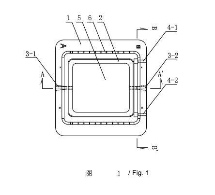
Figure 1 is a schematic diagram of structure of framework;
Figure 2 is an A-A' section view of framework in Figure 1.
Figure 3 is a B-B' section view of framework in Figure 1.
Figure 4 is a schematic diagram of structure of electrode groups in
transparent thin
film
Figure 5 is an amplified schematic diagram of local structure of C part in
Figure 4.
In the figures, 1 refers to framework, 2 refers to bearing edges, 3-1 and 3-2
refer to
inlet and outlet of culture/processing solution, 4-1 and 4-2 are wire
connecting
terminals of electrode groups, 5, 5-1 and 5-2 refer to transparent film
layers, 6 refers
to scale/graduated scale, 7 refers to cell culture/processing chamber, 8 and 9
refer to
omnibus bars of positive and negative electrodes, 10 refers to
platinum/tungsten
points, and I 1 and 12 refer to positive and negative electrodes.
Detailed Description of the Invention
In combination with figures, the invention is further described as follows:
In Figure 1, the processing device is provided with a hollow framework
structure
1, transparent film layers 5 are respectively correspondingly arranged on the
upper
side surface and the lower side surface of the framework, electrode groups
(which are
6
CA 02731294 2011-01-18
not shown in the figure for simplicity, and the specific is shown in Figure 4)
for
producing a low strength electric field are arranged on the transparent film
layer on at
least one side, wire connecting terminals 4-1 and 4-2 of the electrode groups
are
arranged at one end of the framework, an inlet and an outlet 3-1 and 3-2 of
culture/processing solution are correspondingly arranged at two corresponding
ends
of the framework, and sandwich space surrounded by the two transparent film
layers
and the framework constitutes a cell culture/processing chamber.
Wherein the framework is in the shape of a rectangle or a regular polygon,
bearing edges 2 are arranged on the upper side surface and the lower side
surface of
an inner edge of the framework, and the transparent film layers are
bonded/fixedly
connected with the framework into a whole via the bearing edges.
The transparent film layers are transparent plastic thin film layers.
In Figure 2, the inlet and the outlet 3-1 and 3-2 of the culture/processing
solution are
arranged in a framework I body, one end of each is in a converging cone-like
opening
structure, and the other end of each is communicated with the cell
culture/processing
chamber 7.
The sandwich space surrounded by the two transparent film layers 5-1 and 5-2
and the framework constitutes the cell culture/processing chamber 7.
It can be seen from the figure that the cell culture/processing chamber is a
thin-layer
chamber, and the thickness is not more than 2mm.
Further, a scale/graduated scale 6 is arranged on the periphery of the
framework.
In Figure 3, the wire connecting terminals 4-1 and 4-2 of the electrode groups
are
arranged at one end of the framework I and respectively in contact and
connection
with omnibus bars 8 and 9 of positive and negative electrodes (shown in Figure
4)
arranged on the transparent film layer for forming electrical pathways.
The inlet and the outlet of the culture/processing solution are arranged at
two
corresponding ends of the framework, and the outlet 3-2 of the
culture/processing
solution can be just seen in the section view direction shown in the figure.
In Figure 4, the electrode groups are printed circuit copper foil layers which
are
distributed in the transparent film layer 5 or on the surface of the
transparent film
7
CA 02731294 2011-01-18
layer by a structure of leading positive electrodes and negative electrodes 11
and 12 to
be arranged alternately, wherein the positive and the negative electrode
groups are
electrically connected with the wire connecting terminals (see 4-1 and 4-2 in
Figure 4)
positioned at one end of the framework and an external instrument via the
omnibus
bars 8 and 9.
The electrode groups 11 and 12 are arranged in the transparent film layer,
pass
through platinum/tungsten points 10 which are connected with the electrode
groups
and penetrate the surface of the transparent film and further constitute an
electrode
lattice group on the surface of the transparent film.
The distribution structure of the positive and the negative electrodes shown
in the
figure is only the schematic diagram of the structure, when in practical
implementation, the positive and the negative electrodes are not only limited
to the
distribution form shown in the figure, and can adopt the way of arranging them
alternately in a two-and-two way or other forms, in order to obtain the better
electric
field distribution effect.
In addition, the printed circuit copper foil layers constituting the electrode
groups
can be arranged in the same transparent film layer, or be arranged on two
corresponding side surfaces of the same transparent film layer, or be
respectively
correspondingly arranged in two corresponding transparent film layers, or be
respectively correspondingly arranged on certain surfaces of the two
corresponding
transparent film layers, aiming at obtaining the better electric field
distribution effect
or facilitating the processing and the manufacturing.
In Figure 5, the printed circuit copper foil layers 11 are arranged on one
side
surface of the transparent film layer, pass through platinum/tungsten points
10 which
are connected therewith and penetrate the surface of the transparent film 5
and further
constitute the electrode lattice group on the surface of the transparent film.
Due to the adoption of the structural form of the electrode lattice group,
compared
with the prior art, the electric field distribution of the produced low
strength electric
field network is more uniform, and the applied voltage can be as low as
millivolt level,
thereby being safer for target cells and avoiding that the long-time imposing
of the
8
CA 02731294 2011-01-18
acting electric field causes the electrical breakdown injuries to the target
cells.
The implementation of the invention is conductive to realizing the purposes of
effectively introducing or delivering drugs, genes, siRNA, shRNA, proteins,
peptides,
antibodies or other biomedical and therapeutic molecules and preparations into
the
target cells under the environmental condition of the low strength electric
field
network; simultaneously, in addition to having the conventional functions of
the
existing cell culture/processing device, the invention can further monitor and
control
the whole experimental/processing process, be convenient to be observed under
a
microscope as a whole and be conductive to separation and selection of the
culture/processing target cells.
The above embodiments are only used to explain and describe the invention
rather than limiting the technical scheme of the invention; and those of
ordinary skill
in the art shall recognize that any changes and variations within the real
spirit range
can be determined to fall within the protection scope of the claimed
invention.
The invention can be widely applied in the fields of clinical medicine, basic
experiments and bioscience
9