Note: Descriptions are shown in the official language in which they were submitted.
CA 02731426 2011-01-20
WO 2010/014089 PCT/US2008/071650
DATA TRANSLATION SYSTEM AND METHOD
Background of the Invention
1. Field of the Invention
The present invention relates to a data translation system and method, and
more
particularly, to a data translation system and method for performing a non-
linear data
translation.
2. Statement of the Problem
An optocoupler is a device that communicates signals from a first device to a
second device using light. The optocoupler therefore can be used to provide
electrical
isolation, such as between specific components or circuits. The electrical
isolation
advantageously can be used to prevent a component or circuit from drawing
excessive
electrical current. The electrical isolation can further be used to prevent a
short-circuit
or other problem in a device from affecting other devices. Consequently, an
optocoupler is often used for isolating electrical devices and/or electrical
circuits.
One isolation application is employed where a device is located within an
explosive or hazardous environment. An optocoupler can be used to ensure that
the
device does not and cannot draw excessive electrical current and therefore
cannot create
a spark or cause ignition.
An optocoupler has drawbacks. An optocoupler has a relatively slow switching
speed. As a result, an optocoupler has a limited signaling bandwidth. Further,
an
optocoupler is a passive device and does not perform any signal transmission
control or
regulation.
Aspects of the Invention
In one aspect of the invention, a data translation system for performing a non-
linear data translation on a digitized AC signal comprises:
an input for receiving the digitized AC signal;
an output for outputting a non-linearly translated signal; and
a processing system coupled to the input and to the output and configured to
receive the digitized AC signal, non-linearly translate the digitized AC
signal using a
1
CA 02731426 2011-01-20
WO 2010/014089 PCT/US2008/071650
predetermined transfer function to create the non-linearly translated signal,
and transfer
the non-linearly translated signal to the output.
Preferably, the predetermined transfer function creates the non-linearly
translated
signal with respect to a predetermined reference point.
Preferably, the predetermined transfer function is configured to alternatively
compress or amplify digital values of the digitized AC signal.
Preferably, the predetermined transfer function is configured to alternatively
compress or amplify digital values of the digitized AC signal in relation to a
distance
from the predetermined reference point.
Preferably, the non-linear data translation substantially preserves phase
information in the non-linearly translated signal.
Preferably, the non-linear data translation preserves zero-crossing
information in
the non-linearly translated signal.
Preferably, the non-linear data translation substantially reduces a signal
bandwidth of the non-linearly translated signal.
In one aspect of the invention, a data translation method for a digitized AC
signal
comprises:
receiving the digitized AC signal;
non-linearly translating the digitized AC signal using a predetermined
transfer
function to create a non-linearly translated signal; and
transferring the non-linearly translated signal.
Preferably, the predetermined transfer function creates the non-linearly
translated
signal with respect to a predetermined reference point.
Preferably, the predetermined transfer function is configured to alternatively
compress or amplify digital values of the digitized AC signal.
Preferably, the predetermined transfer function is configured to alternatively
compress or amplify digital values of the digitized AC signal in relation to a
distance
from the predetermined reference point.
Preferably, the non-linear data translation substantially preserves phase
information in the non-linearly translated signal.
Preferably, the non-linear data translation preserves zero-crossing
information in
the non-linearly translated signal.
2
CA 02731426 2011-01-20
WO 2010/014089 PCT/US2008/071650
Preferably, the non-linear data translation substantially reduces a signal
bandwidth of the non-linearly translated signal.
In one aspect of the invention, an optocoupler transmission system for
controlling signal transmission through an optocoupler transmission medium
comprises:
an optocoupler; and
a controller coupled to the optocoupler and configured to receive a transmit
attempt from a first device, determine if a second device is already
transmitting through
the optocoupler, determine if receiving the transmit attempt is outside a
deadband period
after a power-up occurrence, and transmit from the first device through the
optocoupler
if the second device is not transmitting and if the deadband period has
elapsed.
Preferably, the controller is further configured to hold off the first device
from
transmitting through the optocoupler until the second device has completed
transmission
if the second device is already transmitting.
Preferably, the controller being is configured to hold off the first device
from
transmitting through the optocoupler until the deadband period has elapsed if
the
transmit attempt is within the deadband period.
Preferably, the optocoupler transmission system includes at least two devices
communicating through the optocoupler.
Preferably, the optocoupler transmission system implements a master-slave
communication scheme.
In one aspect of the invention, a transmission control method for controlling
signal transmission through an optocoupler transmission medium comprises:
receiving a transmit attempt from a first device;
determining if a second device is already transmitting through the optocoupler
transmission medium;
determining if receiving the transmit attempt is outside a deadband period
after a
power-up occurrence; and
transmitting from the first device through the optocoupler transmission medium
if the second device is not transmitting and if the deadband period has
elapsed.
Preferably, the method further comprises holding off the first device from
transmitting through the optocoupler transmission medium until the second
device has
completed transmission if the second device is already transmitting.
3
CA 02731426 2011-01-20
WO 2010/014089 PCT/US2008/071650
Preferably, the method further comprises holding off the first device from
transmitting through the optocoupler transmission medium until the deadband
period
has elapsed if the transmit attempt is within the deadband period.
Preferably, the optocoupler transmission medium includes at least two devices
communicating through the optocoupler transmission medium.
Preferably, the method implements a master-slave communication scheme.
Description of the Drawings
The same reference number represents the same element on all drawings. It
should be understood that the drawings are not necessarily to scale.
FIG. 1 shows a bus loop system according to an embodiment of the invention.
FIG. 2 shows greater detail of an isolation feature of the signal processor
according to an embodiment of the invention.
FIG. 3 shows a translation system for performing a data translation on a
digitized
AC signal according to an embodiment of the invention.
FIG. 4 shows a transfer function according to an embodiment of the invention.
FIG. 5 shows an AC signal at the input of the translation system.
FIG. 6 shows the digitized AC signal after non-linear data translation
according
to the invention.
FIG. 7 is a flowchart of a data translation method for a digitized AC signal
according to an embodiment of the invention.
FIG. 8 shows a prior art optocoupler communication system that performs
duplex communications through an optocoupler transmission medium between
device A
and device B.
FIG. 9 shows an optocoupler communication system according to an
embodiment of the invention.
FIG. 10 shows further detail of the optocoupler communication system according
to an embodiment of the invention.
FIG. 11 is a flowchart of a transmission control method for controlling signal
transmission through an optocoupler transmission medium according to an
embodiment
of the invention.
4
CA 02731426 2015-07-13
Detailed Description of the Invention
FIGS. 1-11 and the following description depict specific examples to teach
those
skilled in the art how to make and use the best mode of the invention. For the
purpose of
teaching inventive principles, some conventional aspects have been simplified
or omitted.
Those skilled in the art will appreciate variations from these examples that
fall within the
scope of the invention. Those skilled in the art will appreciate that the
features described
below can be combined in various ways to form multiple variations of the
invention. As a
result, the invention is not limited to the specific examples described below,
but only by the
claims and their equivalents.
FIG. 1 shows a bus loop system 5 according to an embodiment of the invention.
The
bus loop 5 includes a host system 1, a bus loop 4, a bus instrument 10, and a
signal
processor 30 coupling the bus instrument 10 to the bus loop 4. The host system
1 generates
a loop voltage VL and a loop current IL over the bus loop 4. The host system 1
may
comprise a central control unit, a CPU, or some other processing system used
to process the
signals received over the bus loop 4. According to one embodiment of the
invention, the
bus loop 4 comprises a two-wire bus loop 4. However, it should be understood
that the bus
loop 4 does not have to comprise a two-wire bus loop.
The bus instrument 10 can include any manner of sensor or meter, such as a
flow
meter. In embodiments where the bus instrument 10 includes a flow meter, the
flow meter
may comprise a vibratory flow meter, such as a Coriolis flow meter or a
densitometer. As
shown in FIG. 1, the bus instrument 10 includes a sensor 13 and bus instrument
electronics
20. The bus instrument electronics 20 may comprise any manner of CPU,
processing
system, or micro-processing system. According to an embodiment of the
invention, the
sensor 13 is configured to generate first analog signals and input the first
analog signals to
the bus instrument electronics 20. The bus instrument electronics 20 can
generate second
analog signals that are in the form of a variable loop current IL flowing in
the bus loop 4.
The bus instrument 10 can be configured to draw a predetermined or limited
amount of
power when in use with the two-wire bus 4. Because of the measurement
communication
protocol and thc power limitations built into the bus loop system 5, the bus
instrument 10
may be isolated from the two-wire bus loop 4 using a signal processor 30. In
some
embodiments, the signal processor 30 can comprise an intrinsically safe (I.S.)
barrier
(dashed line).
5
CA 02731426 2011-01-20
WO 2010/014089 PCT/US2008/071650
The isolation limits the electrical power that the bus instrument 10 can draw
from
the two-wire bus loop 4 and the host system 1. The isolation prevents damage
to the
two-wire bus loop 4 and the host system 1 upon the event of catastrophic
failure of the
bus instrument 10. In addition, the isolation limits electrical power transfer
through the
I.S. barrier in order to eliminate an explosion hazard and prevent ignition of
any
explosive or flammable materials in the environment of the bus instrument 10.
FIG. 2 shows greater details of an isolation feature of the signal processor
30
according to an embodiment of the invention. The signal processor is shown as
receiving a first analog signal from the bus instrument 10. However, it should
be
understood that the first analog signal does not have to originate from the
bus instrument
10, but rather, the signal processor 30 may be utilized in other environments
where
analog signal processing is required. The analog signal received from bus
instrument 10
over leads 220 are received by an analog to digital converter 240 where the
signals are
digitized. According to one embodiment of the invention, the analog-to-digital
converter 240 comprises a delta sigma converter, which converts the analog
signal into a
serial bit stream. However, it should be understood that other analog-to-
digital
converters may be used and the particular analog-to-digital converter used
should not
limit the scope of the invention.
According to an embodiment of the invention, the signal processor 30 includes
an optocoupler 115 that is connected between the two-wire bus loop 4 and the
analog-
to-digital converter 240. The optocoupler 115 may also be referred to as an
opto-
isolator, optical coupler, or photocoupler. The optocoupler 115 electrically
isolates the
bus instrument 10 from the host system 1. Consequently, the bus instrument 10
cannot
short out the two-wire bus loop 4. Furthermore, catastrophic failure of the
bus
instrument 10 cannot draw excessive current from the host system 1. The
optocoupler
115 comprises a transmitter light source 122 and a receiver light source 123.
The
transmitter and receiver light sources 122, 123 can comprise any manner of
light-
reactive electronic components, including laser transmitter and receiver light
sources,
LED transmitter and receiver light sources, LED laser transmitter and receiver
light
sources, etc.
The transmitter light source 122 and the receiver light source 123 are
commonly
formed adjacent to each other wherein light generated by the transmitter light
source
6
CA 02731426 2011-01-20
WO 2010/014089 PCT/US2008/071650
122 is directly received by the receiver light source 123. In other
embodiments, the
transmitter light source 122 and the receiver light source 123 are separated
by some
optical device, such as a fiber optic cable, for example. In some embodiments,
the two
components are formed into a single package as shown in FIG. 2. However, it
should be
understood that in other embodiments the transmitter light source 122 and the
receiver
light source 123 may comprise separate components.
The transmitter light source 122 generates a light-encoded signal that
comprises
a conversion of electrical current into emitted light. The receiver light
source 123
receives the light-encoded signal and converts the received light back into an
electrical
signal that is substantially identical to the original electrical signal at
the transmitter
light source 122. The optocoupler 115 is therefore well suited for
transferring digital
signals.
In the embodiment shown in FIG. 2, the bus instrument 10 generates a first
analog signal, which is sent to the analog-to-digital converter 240. The
analog-to-digital
converter 240 outputs a digital signal. The digital signal is received by the
transmitter
light source 122 and sent to the receiver light source 123. The receiver light
source 123
can then transmit the received signal to a signal conditioner 250.
The signal conditioner 250 can process the digital signals, which may be in
the
form of a serial bit stream, for example and convert the digital signal into a
scaled pulse
width modulation (PWM) signal. The PWM signal can then be converted into a
second
analog signal and output to the bus loop 4.
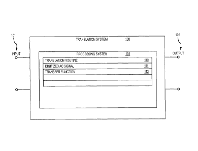
FIG. 3 shows a translation system 100 for performing a non-linear data
translation on a digitized AC signal according to an embodiment of the
invention. The
translation system 100 includes one or more inputs 101 and one or more outputs
102.
The translation system 100 receives the digitized AC signal at the input 101
and outputs
a translated signal at the output 102. The translated signal can be translated
into a form
that is more efficient and usable for transmission over a transmission medium,
such as
transmission through the optocoupler 115, for example. However, other
transmission
media are contemplated and are within the scope of the description and claims.
The translation system 100 is configured to receive the digitized AC signal,
non-
linearly translate the digitized AC signal using a predetermined transfer
function to
create a translated signal portion, and transfer the translated signal
portion. The
7
CA 02731426 2011-01-20
WO 2010/014089 PCT/US2008/071650
translation system 100 can translate the digitized AC signal with respect to a
predetermined reference point. The translation system 100 can translate the
digitized
AC signal with respect to a distance from the predetermined reference point,
such as a
vertical distance (i.e., voltage) from the reference point.
The translation system 100 can comprise any manner of system, including a part
of the signal processor 30 or other barrier device, an analog-to-digital (AID)
converter, a
processor or microprocessor, a pre-processor, etc. Alternatively, in some
embodiments
the translation system 100 can comprise a portion or subsystem of the bus
instrument
10.
The translation system 100 can include a processing system 104 and storage
(not
shown). The processing system 104 can include a translation routine 110, a
digitized
AC signal storage 111 (or storage for at least a portion of the digitized AC
signal, such
as a signal portion), and a predetermined transfer function 112. The
predetermined
transfer function 112 is employed to process the digitized AC signal or signal
portion
thereof and perform the non-linear translation of the signal portion (see
discussion
below).
FIG. 4 shows a transfer function according to an embodiment of the invention.
The transfer function is non-linear, including both compression and
amplification. This
is shown in the legends above the graph. Further, in some embodiments the
compression and amplification can also be non-linear.
The transfer function modifies the digitized AC signal, such as by adjusting
specific values or regions, yet without changing the overall shape of the
input
waveform. The transfer function can comprise a mathematical function that
translates
the digitized AC signal. Alternatively, the transfer function can comprise a
series of
coefficients that are multiplied by the digitized AC signal, essentially a
digital filter.
The digitized AC signal is translated in order to improve the transfer of the
digitized AC
signal and in order to improve the efficiency of the transfer. The data
translation
enhances transmission by limiting bandwidth. The data translation retains
phase
information and advantageously retains the phase information while decreasing
bandwidth. The data translation achieves this by both compressing and
amplifying the
digitized AC signal.
8
CA 02731426 2011-01-20
WO 2010/014089 PCT/US2008/071650
In some embodiments, the digitization can comprise a digital communication
protocol that is imposed onto a time-varying AC signal, such as on an analog
measurement signal. For example, a HART digital communication protocol can be
superimposed on an analog voltage or analog current signal. The HART protocol
in
some embodiments can employ a Continuous Phase Frequency-Shift Keying (CP-FSK)
modulation. However, it should be understood that other communication
protocols and
modulations are contemplated and are within the scope of the description and
claims.
The transfer function performs amplification on input values that are within a
specified distance of a reference point. One reference point can be an AC
signal zero-
crossing point, even where the zero-crossing point has been shifted above or
below a
zero voltage level. However, other reference points are contemplated and are
within the
scope of the description and claims.
The amplification can achieve a predetermined gain. The amplification can be
substantially linear or can be non-linear. In some embodiments, the gain can
vary with
distance from the reference point. The amplification around the reference
point
preserves the zero-crossing information. The amplification around the
reference point
can make zero-crossing discrimination easier.
Conversely, the transfer function performs compression on a signal portion
that
is more than the predetermined distance from the reference point, such as the
previously
discussed zero-crossing point. The compression can be substantially linear or
can be
non-linear. The compression can achieve a predetermined compression. In some
embodiments, the compression can vary with a distance from the reference
point.
FIG. 5 shows an AC signal at the input of the translation system 100. The AC
signal comprises a time-varying signal including an amplitude and period. The
AC
signal can be already digitized or alternatively in some embodiments can be
digitized by
the translation system 100 before translation.
FIG. 6 shows the digitized AC signal after non-linear data translation
according
to the invention. It can be seen from this figure that the overall peak-to-
peak amplitude
of the AC signal has been significantly reduced and compressed without
changing the
waveform shape. In this example, the original AC signal has been compressed
from an
original amplitude of about 250 down to an amplitude of about 30. However, at
the
same time the amplitude around the reference point, which here is a zero-
crossing point
9
CA 02731426 2011-01-20
WO 2010/014089 PCT/US2008/071650
(even though the amplitude is not zero), has been amplified. In contrast to
the
compressed regions where the digital values are about one unit apart
vertically, in the
amplified region around the reference point the digital values are about three
units apart.
This is done so that the reference points in the digitized AC signal doe not
become
closer together and harder to discriminate, such as if the signal regions
around the
reference point had been compressed. Compressed digital values may be
difficult to
determine, especially in the presence of noise superimposed onto the digital
values.
The end result is that digital values away from the reference point (such as
near
the peaks) are relatively close in terms of vertical distance as a result of
the
compression. Conversely, the digital values around the reference point are
moved
vertically apart by the amplification. The result is that the reference points
are easier to
discriminate while the overall AC signal requires less overall bandwidth.
FIG. 7 is a flowchart 700 of a data translation method for a digitized AC
signal
according to an embodiment of the invention. In step 701, the digitized AC
signal is
received.
In step 702, the digitized AC signal is non-linearly translated. Using the
transfer
function, the signal away from a reference point is compressed (i.e., large
digital values
are compressed). The compression can be of any desired amount and can employ
any
desired compression. The compression of the signal portion in this voltage
region
operates to reduce the bandwidth of the digitized AC signal and makes the
transmission
of the digitized AC signal through the optocoupler more efficient. Further
using the
transfer function, the signal close to the reference point is amplified by a
predetermined
gain (i.e., small digital values are amplified). The amplification can be by
any desired
gain amount. The amplification preserves the phase information, including the
phase
information provided by zero crossings of the digitized AC signal. Further,
the
amplification can make the zero crossing points easier to discriminate in the
digitized
AC signal after the digitized AC signal passes through the optocoupler.
In step 703, after the signal portion is compressed/amplified, the non-
linearly
translated signal is transferred to the optocoupler for transmission. After
transmission,
the phase information can be determined from the non-linearly translated
signal,
including the zero-crossing information. Further, if desired, the compression
and
amplification can optionally be reversed after the transmission, such as by
using a
CA 02731426 2011-01-20
WO 2010/014089 PCT/US2008/071650
mirror-image (i.e., reverse) transfer function. Subsequently, the method can
loop back
up to step 701 and iteratively receive and process signal portions.
FIG. 8 shows a prior art optocoupler communication system that performs
duplex communications through an optocoupler transmission medium between
device A
and device B. The optocoupler transmission medium includes an optocoupler and
associated wires or other conductors. Two separate transmission paths are
included so
that duplex communications (i.e., communications in both directions) can be
performed.
In some embodiments, the communications comprise half-duplex communications
wherein only one device can transmit at a time.
The prior art optocoupler communication system has drawbacks. Both device A
and device B can attempt to communicate at the same time. Simultaneous
communication attempts in a half-duplex communication system will result in a
failure
of transmission. Further, if a transmission from device A creates an echo back
to device
A, then device A can misinterpret the received echo as a legitimate
transmission from
device B.
FIG. 9 shows an optocoupler communication system 900 according to an
embodiment of the invention. The optocoupler communication system 900 includes
a
controller 920 that regulates communications between device A 905 and device B
907
through a transmission medium including the optocoupler 115. The optocoupler
115 in
some embodiments performs half-duplex (or simplex) communication between
devices,
wherein only one device can transmit at a time.
It should be understood that the controller 920 can be located anywhere in the
optocoupler communication system 900 and is shown at the right of the
optocoupler 115
merely for illustration. In some embodiments, the controller 920 can comprise
a
component of the signal processor 30. Further, the controller 920 in some
embodiments
can comprise a component of device A 905 or device B 907, wherein the device
operates like a master communication device. At the same time, the other
device(s)
operates as a slave communication device(s).
The optocoupler communication system 900 is configured to prevent the
reception of echoes. Alternatively or in addition, the optocoupler
communication
system 900 is configured to prevent more than one device from transmitting at
a time.
11
CA 02731426 2011-01-20
WO 2010/014089 PCT/US2008/071650
The optocoupler communication system 900 in some embodiments is configured
to receive a transmit attempt from a first device A 905, determine if a second
device B
907 is already transmitting through the optocoupler 115, determine if
receiving the
transmit attempt is outside a deadband period after a power-up occurrence, and
transmit
from the first device A 905 through the optocoupler 115 if the second device B
907 is
not transmitting and if the deadband period has elapsed.
FIG. 10 shows further detail of the optocoupler communication system 900
according to an embodiment of the invention. In this embodiment, the
controller 920
and the optocoupler 115 are combined into one device. The combined device can
include additional capabilities and additional circuitry. The controller 920
can include
switches 931 and 932 that are switched by the controller 920 in order to
regulate
transmission through the optocoupler 115. The switches can comprise any manner
of
switches.
FIG. 11 is a flowchart 1100 of a transmission control method for controlling
signal transmission through an optocoupler transmission medium according to an
embodiment of the invention. In step 1101, a transmit attempt is received from
a device
such as device A. It should be understood that the transmit attempt can be
from any
device, but device A is used in this figure and example for purposes of
clarity.
In step 1102, it is determined whether device B is already transmitting. If
device
B is already transmitting, then the method proceeds to step 1103. If device B
is not
already transmitting, then the method branches to step 1105.
In step 1103, where device B is already transmitting, device A is held off
from
transmitting. The holding off is done until device B has completed
transmitting.
In step 1104, the method holds off other transmission attempts until the
transmission from device B is complete. The transmission can comprise a
transmission
from device B to device A in some embodiments, although other devices are
contemplated and are within the scope of the description and claims.
In step 1105, where device B was not already transmitting, the method checks
to
see if the attempt is outside of a deadband. If the transmit attempt is not
outside of the
deadband, then the method loops back up to step 1101 and all transmissions are
held off
until the deadband period has elapsed. If instead the transmit attempt is
outside the
deadband, then the method proceeds to step 1106.
12
CA 02731426 2011-01-20
WO 2010/014089 PCT/US2008/071650
For some bus instruments, during a power-up phase the instrument may generate
and put out measurements or other data that are not within specifications and
should not
be transmitted. For this reason, the method can implement a deadband period
for a
predetermined time after power-up. Signals received during this deadband
period can
be judged unreliable and can be ignored. Signals arriving after the deadband
has
expired are judged acceptable.
In step 1106, device B is held off from transmitting. This can include
additional
devices if more that two devices can transmit through the optocoupler
transmission
medium.
In step 1107, device A is allowed to transmit.
In step 1108, the method checks to see if device A is done transmitting. If
device A is
not done transmitting, the method loops back to step 1106. If (and when)
device A is
done transmitting, then the method loops back up to step 1101 and waits for
further
transmit attempts.
13