Note: Descriptions are shown in the official language in which they were submitted.
CA 02731693 2013-10-23
Two-Sided Splice for High Temperature Superconductor Laminated Wires
[0001] This application claims the benefit of U.S. Utility Application No.
12/178469, filed July
23, 2008.
[0002] This invention was made with Government support under Agreement No.:
HSHQDC-08-
9-00001. The Government has certain rights in the invention.
Technical Field
[0003] This application relates to the field of high temperature
superconductors.
Background
[0004] High temperature superconductor (HTS) materials provide a means for
carrying
extremely large amounts of current with extremely low loss. HTS materials lose
all resistance to
the flow of direct electrical current and nearly all resistance to the flow of
alternating current
when cooled below a critical temperature. The development of HTS wires (the
expression
"wires" is used here for a variety of conductors, including tape-like
conductors) using these
materials promises a new generation of high efficiency, compact, and
environmentally friendly
electrical equipment, which has the potential to revolutionize electric power
grids, transportation,
materials processing, and other industries. However, a commercially viable
product has stringent
engineering requirements, which has complicated the implementation of the
technology in
commercial applications.
[0005] In second generation HTS wire (coated conductor) technology, currently
under
development, the HTS material is generally a polycrystalline rare-
earth/alkaline-earth/copper
oxide, e.g. yttrium-barium-copper oxide (YBCO). The current carrying
capability of the HTS
material is strongly related to its crystalline alignment or texture. Grain
boundaries formed by the
misalignment of neighboring crystalline superconductor grains are known to
form an obstacle to
superconducting current flow, but this obstacle decreases with the increasing
degree of alignment
or texture. Therefore to make the material into a commercially viable product,
e.g. an
1
CA 02731693 2011-01-20
WO 2010/011739
PCT/US2009/051392
HTS wire, the superconducting material must maintain a high degree of
crystalline
alignment or texture over relatively long distances. Otherwise, the
superconducting
current carrying capacity (critical current density) will be limited.
[0006] A schematic of a typical second-generation HTS wire 100 is shown
in
Fig. 1. The wire includes substrate 110, buffer layer 120 (which could include
multiple buffer layers), superconductor layer 130, and gap or cap layer 140,
and is
fabricated as described below. It should be noted that in this and all
subsequent
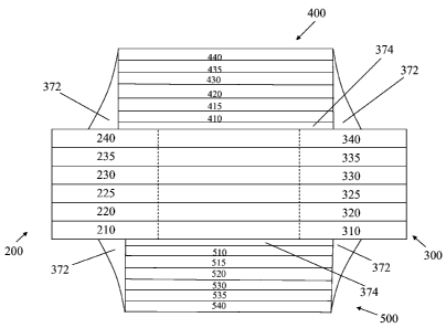
figures, the dimensions are not to scale. Superconductor materials can be
fabricated
with a high degree of crystallographic alignment or texture over large areas
by
growing a thin layer 130 of the material epitaxially on top of a flexible tape-
shaped
substrate 110 and buffer layer 120, which are fabricated so that the surface
of the
topmost layer has a high degree of crystallographic texture at its surface.
When the
crystalline superconductor material is grown epitaxially on this surface, its
crystal
alignment grows to match the texture of the substrate. In other words, the
substrate
texture provides a template for the epitaxial growth of the crystalline
superconductor
material. Further, the substrate provides structural integrity to the
superconductor
layer.
[0007] Substrate 110 and/or buffer 120 can be textured to provide a
template
that yields an epitaxial superconductor layer 130 with excellent
superconducting
properties such as high critical current density. Materials such as nickel,
copper,
silver, iron, silver alloys, nickel alloys, iron alloys, stainless steel
alloys, and copper
alloys can be used, among others, in the substrate. Substrate 110 can be
textured
using a deformation process, such as one involving rolling and
recrystallization
annealing the substrate. An example of such a process is the rolling-assisted
biaxially textured substrate (RABiTS) process. In this case large quantities
of metal
can be processed economically by deformation processing and annealing and can
achieve a high degree of texture.
[0008] One or more buffer layers 120 can be deposited or grown on the
surface
of substrate 110 with suitable crystallographic template on which to grow the
superconductor layer 130. Buffer layers 120 also can provide the additional
benefit
of preventing diffusion over time of atoms from the substrate 110 into the
crystalline
2
CA 02731693 2011-01-20
WO 2010/011739
PCT/US2009/051392
lattice of the superconductor material 130 or of oxygen into the substrate
material.
This diffusion, or "poisoning," can disrupt the crystalline alignment and
thereby
degrade the electrical properties of the superconductor material. Buffer
layers 120
also can provide enhanced adhesion between the substrate 110 and the
superconductor layer 130. Moreover, the buffer layer(s) 120 can have a
coefficient
of thermal expansion that is well matched to that of the superconductor
material.
For implementation of the technology in commercial applications, where the
wire
may be subjected to stress, this feature is desirable because it can help
prevent
delamination of the superconductor layer from the substrate.
[0009] Alternatively, a non-textured substrate 110 such as HASTELLOY, a
corrosion resistant alloy manufactured by Haynes International, Inc. (Kokomo,
In)
can be used, and textured buffer layer 120 deposited by means such as the ion-
beam-
assisted deposition (IBAD) or inclined substrate deposition (ISD). Additional
buffer
layers 120 may be optionally deposited epitaxially on the IBAD or ISD layer to
provide the final template for epitaxial deposition of an HTS layer 130.
[0010] By using a suitable combination of a substrate 110 and one or more
buffer layers 120 as a template, superconductor layer 130 can be grown
epitaxially
with excellent crystal alignment or texture, also having good adhesion to the
template surface, and with a sufficient barrier to poisoning by atoms from the
substrate. The superconductor layer 130 can be deposited by any of a variety
of
methods, including the metal-organic deposition (MOD) process, metal-organic
chemical vapor deposition (MOCVD), pulsed laser deposition (PLD), thermal or e-
beam evaporation, or other appropriate methods. Lastly, a cap layer 140 can be
added to the multilayer assembly, which helps prevent contamination of the
superconductor layer from above. The cap layer 140 can be, e.g., silver or a
silver-
gold alloy, and can be deposited onto the superconductor layer 130 by, e.g.,
sputtering. In the case where slitting is performed after lamination, the cap
layer
may also include an additional laminated metal "stabilizer" layer, such as a
copper
or stainless steel layer, bonded to the cap layer, e.g., by soldering, forming
a gap
layer.
3
CA 02731693 2011-01-20
WO 2010/011739
PCT/US2009/051392
[0011] An exemplary as-fabricated multilayer HTS wire 100 includes a
biaxially
textured substrate 110 of nickel with 5% tungsten alloy; sequentially
deposited
epitaxial buffer layers 120 of Y203, yttria stabilized zirconia ("YSZ"), and
Ce02;
epitaxial layer 130 of YBCO; and a gap layer 140 of Ag. Exemplary thicknesses
of
these layers are: a substrate of about 25-75 micrometers, buffer layers of
about 75
nm each, an YBCO layer of about 1 micrometer, and a gap layer of about 1-3
micrometers. HTS wires 100 as long as 100 m have been manufactured thus far
using techniques such as those described above.
[0012] During use, it is desirable that the HTS wire is able to tolerate
bend
strains. A bend induces tensile strain on the convex outer surface of the
bend, and
compressive strain on the concave inner surface of the bend, thereby
subjecting the
HTS layer to tensile or compressive strains depending on the direction in
which the
wire is bent. While a modest amount of compressive stress can actually enhance
the
current carrying capacity of an HTS layer, in general subjecting the whole
assembly
to stress (especially repeated stress) places the wire at risk of mechanical
damage.
For example, cracks could be formed and propagate in the HTS layer, degrading
its
mechanical and electrical properties, or the different layers could delaminate
from
each other or from the substrate.
[0013] Methods for reducing stress in the HTS layer are described, e.g.,
in U.S.
Patent No. 6,745,059 and U.S. Patent No. 6,828,507. For example, a copper
strip,
chosen to have similar thickness and mechanical features to the substrate, can
be
bonded onto the upper surface of the insert. This sandwiches the HTS layer
roughly
in the middle of the overall structure, so if the assembly is bent, the HTS
layer is
neither at the outer nor inner surface of the bend. Two of these assemblies
can also
be bonded together at their respective copper strips to form a single HTS wire
assembly. In this case, the two substrates face outward, and the copper tapes
are in
the middle of the assembly. In this case the inclusion of a second assembly
provides
additional current carrying capacity; however, electrical contact to the HTS
layers
requires splicing the wire open, or partially removing one of the inserts in
the
contact section.
4
CA 02731693 2011-01-20
WO 2010/011739
PCT/US2009/051392
[0014] A further issue for coated conductor HTS wires is that of
environmental
contamination when the wire is in use. Environmental exposure can slowly
degrade
the electrical performance of HTS layers. Also, in the presence of cryogenic
liquids
such as liquid nitrogen in contact with the wire, the liquid can diffuse into
pores
within the wire, and on warming can form "balloons" that can damage the wire.
Sealing the wire is desirable to prevent either environmental exposure of the
HTS
layers or penetration of the liquid cryogen into the wire. Seals for HTS
assemblies
are described in, e.g. U.S. Patent No. 6,444,917.
[0015] The coated conductor approach has been greatly advanced in recent
years
to the point where long length manufacturing of reinforced tapes is being
established. However, the utility of these tapes would be greatly increased if
they
could be made to any required length via low resistance joints that are
mechanically
robust and conform to tight geometric tolerances.
[0016] HTS wires must be joined in the field to each other and to
terminations
and leaders. As well, yield and wire quality can improve with factory
splicing,
thereby reducing wire price and enabling shipment of wires of lengths beyond
inherent manufacturing limits. These splices must meet similar requirements as
the
wire.
[0017] Early splices were lap joints. A lap joint is a process of joining
two
pieces of material by overlapping them. Thus, in the case of HTS wires, two
HTS
wires can be joined by overlapping the ends of the wires over a set distance
and then
soldering the wires together. The lap joint method creates a splice that is
about 2.0
to 2.2 times the thickness of the original wire.
[0018] Although the lap method is feasible for first generation wires or
tapes, the
second generation tape, where the insulating layer is between the YBCO film
and
substrate, requires the use of a face¨to¨face strap or a conductive bridge
with a lap
joint at each end to retain the original orientation of the parent wire being
spliced
and to minimize splice resistance. Co-pending U.S. application Ser. No.
11/880,586
discloses the conductive bridge splice in greater detail and the disclosure of
which is
hereby incorporated by reference in its entirety. However, the conductive
bridge
CA 02731693 2011-01-20
WO 2010/011739
PCT/US2009/051392
structure takes twice as long to make as the simple lap joint, because
essentially two
laps joints must be made, e.g. one for each end of the strap, doubles splice
resistance, and introduces two lumps in the wire per splice. As with first
generation
wire, if the conductive bridge is the same material as the parent, then the
splice will
typically be 2.0 to 2.2 times the thickness of the parent wire. The splice
should be
similar in thickness and mechanical properties to the parent wire the better
for
cabling, as a stiffer thick region requires greater tension in cabling
increases the
likelihood of splice splitting in bending, and as short a length as possible
to
minimize local deviations from cable pitch. These issues are aggravated by the
need
for thicker lamination strips for adequate wire stabilization in the cable.
Therefore, a
need exists for a physically and mechanically near symmetric (two-sided),
mechanically robust, yet compliant, splice that requires only one joint per
splice,
while still preserving the mechanical and electrical properties of each of the
spliced
wires.
Summary
[0019] In view of these considerations, one or more embodiments relate to
a
splice technique that is twice as fast to make than techniques used to make a
double
lap conductive bridge splice, provides a wire with symmetric mechanical
response
about its axis and improves splice robustness while reducing splice stifthess.
[0020] Two-sided, low cost, low resistance, mechanically robust, thin and
geometrically uniform joints for thick superconductor wires are described.
[0021] The embodiments disclosed herein relate to a two-sided joint for a
HTS
laminated wire, where the two-sided joint includes: a first laminated HTS wire
having a tapered end across the width of the first laminated wire and
comprising a
first laminate layer, a substrate layer overlaying the first laminate layer, a
buffer
layer overlaying the substrate layer, a superconductor layer overlaying the
buffer
layer, a gap layer overlaying the superconductor layer, and a second laminate
layer
overlaying the gap layer; a second laminated HTS wire having a tapered end
across
the width of the second laminated wire and comprising a first laminate layer,
a
substrate layer overlaying the first laminate layer, a buffer layer overlaying
the
6
CA 02731693 2011-01-20
WO 2010/011739
PCT/US2009/051392
substrate layer, a superconductor layer overlaying the buffer layer, a gap
layer
overlaying the buffer layer, and a second laminate layer overlaying the gap
layer,
wherein the tapered end of the first laminated HTS wire is adjacent to and
mated
with the tapered end of the second laminated HTS wire; a first HTS strap in
electrical communication with the second laminate layer of the first laminated
HTS
wire and the second laminate layer of the second laminated HTS wire; and a
backing
strap proximate to the first laminate layer of the first laminated HTS wire
and the
first laminate layer of the second laminated HTS wire.
[0022] The first HTS strap can include a gap layer, a superconductor
layer
overlaying the gap layer, a buffer layer overlaying the superconductor layer,
and a
substrate layer overlaying the buffer layer, wherein the gap layer is adjacent
to and
in electrical communication with the second laminate layer of the first
laminated
HTS wire and the second laminate layer of the second laminated HTS wire.
Additionally, the first HTS strap can include a laminate layer overlaying the
substrate layer and/or a second laminate layer interposed between the
electrically
conductive gap layer and the first and second HTS wires.
[0023] The backing strap can be selected to be within about 50 % and about 150
% or about 90% to about 105% of the thickness of the first HTS strap and/or
can
include a metal or alloy containing aluminum, zinc, copper, silver, nickel,
iron,
chrome, lead, silver or molybdenum. Additionally, the backing strap can be a
second HTS strap. The second HTS strap can include a substrate layer, a buffer
layer overlaying the substrate layer, a superconductor layer overlaying the
buffer
layer, and a gap layer overlaying the superconductor layer, wherein the gap
layer is
adjacent to and in electrical communication with the first laminate layer of
the first
laminated HTS wire and the first laminate layer of the second laminated HTS
wire.
The second HTS strap can further include a laminate layer proximate to the
substrate
layer and/or a second laminate layer interposed between the electrically
conductive
gap layer and the first and second HTS wires. Additionally, the backing strap
can be
selected such that a first load to impart a 0.5% tensile strain in the backing
strap is
within a 30% to 150% range of a second load required to impart a 0.5% tensile
strain to the first HTS strap. Further, the backing strap and the first HTS
strap can
7
CA 02731693 2011-01-20
WO 2010/011739
PCT/US2009/051392
be selected such that a first load required to impart 0.5% tensile strain in
the backing
strap and the first HTS strap combined is less than a second load required to
impart
0.5% strain in either of the first laminated wire or the second laminated HTS
wire.
[0024] In one or more embodiments, the electrical communication can include a
metal or alloy with a melting temperature below 240 degrees C and the metal or
alloy can have an ambient temperature resistivity below 50 micro-ohm-cm.
Additionally, the metal or alloy can contain any one of Pb, Sn, Ag, Cu or In.
[0025] In one or more embodiments, the first laminated HTS wire and the second
laminated HTS wire each further include a non-laminated HTS wire interposed
between the first laminate layer and the substrate layer, wherein the non-
laminated
HTS wire comprises a second gap layer overlaying the first laminate layer, a
second
HTS film layer overlaying the gap layer, a second buffer layer overlaying the
second
HTS film layer, and a second substrate layer overlaying the second buffer
layer,
wherein the gap layer of the non-laminated HTS wire is in electrical
communication
with the first laminate layer. Additionally, a second HTS strap can be in
electrical
communication with the first laminate layer.
[0026] In some embodiments, the first laminated HTS wire and the second
laminated HTS wire each have a thickness greater than or equal to about 250
micrometers or greater than or equal to about 300 micrometers. Further, the
first
HTS strap can have a thickness of less than about 250 micrometers or about 50
micrometers to about 200 micrometers. In some embodiments, the first HTS strap
can be between about 2% to about 70% longer than the length of the backing
strap
and/or about 20% to about 50% longer than the length of the backing strap.
[0027] In some embodiments, the angle of each of the tapered first ends
relative to
the thick laminated wire ranges from about 3 degrees to about 50 degrees.
Further,
the length of the tapered ends can range about 0.4 cm to about 10 cm. The HTS
strap
can have a length from about 2 cm to 26 cm or from about 5 cm to 26 cm. The
backing strap can have a length from about 6 cm to about 16 cm or from about
1.5
cm to 25 cm.
8
CA 02731693 2011-01-20
WO 2010/011739
PCT/US2009/051392
[0028] In one or more embodiments, the laminate of the each laminated wire can
be selected from a material consisting of brass, stainless steel, copper or
alloys
containing zinc, lead, silver, tin, nickel, iron, and aluminum.
[0029] In one or more embodiments, the resistance through the joint can be
less
than 3.0 micro ohms in the 77 K to 293 K temperature range.
[0030] In one or more embodiments, bending the two-sided joint on a diameter
of
cm or less does not produce a physical kiffl( in the joint, does not reduce
critical
current by more than 15 %, does not increase joint resistance by more than 5
%.
Further, spiral winding the two-sided joint onto a former, wherein the former
has a
diameter 5 cm or less, with an axial tension in the first and second thick
laminated
wires of less than 1 kg to 5 kg and a pitch of at least 65 mm such that a gap
between
the two-sided joint and former is less than 1.5 mm
[0031] In one or more embodiments, the two-sided joint for an HTS laminated
wire includes: a first laminated HTS wire having a tapered first end across
the width
of the first laminated HTS wire and comprising a first laminate layer, a
substrate
layer overlaying the first laminate layer, a HTS film layer overlaying the
substrate
layer; and a second laminate layer overlaying the HTS film layer; a second
laminated HTS wire having a tapered first end across the width of the second
laminated HTS wire and comprising a first laminate layer, a substrate layer
overlaying the first laminate layer, a HTS film layer overlaying the substrate
layer,
and a second laminate layer overlaying the HTS film layer, and wherein the
tapered
first end of the first laminated HTS wire is adjacent to and mated with the
angled
tapered end of the second laminated HTS wire; an upper support in electrical
communication with second laminate of the first laminated HTS wire and the
second
laminate layer of the second laminated HTS wire; and a lower support proximate
to
the first laminate layer of the first laminated HTS wire and the first
laminate layer of
the second laminated HTS wire, wherein the materials and dimensions of the
joint
are selected to provide a neutral axis for the HTS films in the first
laminated HTS
wire and the second laminated HTS wire.
9
CA 02731693 2011-01-20
WO 2010/011739
PCT/US2009/051392
[0032] In one or more embodiments, the two-sided joint for a HTS
laminated
wire includes: a first laminated HTS wire having a tapered first end and
comprising
a first laminate layer, a substrate layer overlaying the first laminate layer,
a HTS
film layer overlaying the substrate layer; and a second laminate layer
overlaying the
HTS film layer; a second laminated HTS wire having a tapered first end and
comprising a first laminate layer, a substrate layer overlaying the first
laminate
layer, a HTS film layer overlaying the substrate layer, and a second laminate
layer
overlaying the HTS film layer, and wherein the tapered first end of the first
laminated HTS wire is adjacent to and mated with the tapered end of the second
laminated HTS wire; a first HTS strap in electrical communication with the
second
laminate layer of the first laminated HTS wire and the second laminate layer
of the
second laminated HTS wire; and a backing strap proximate to the first laminate
layer
of the first laminated HTS wire and the first laminate layer of the second
laminated
HTS wire, wherein the materials and dimensions of the joint are selected to
provide
a continuity of mechanical stress across the joint.
[0033] Another aspect relates to a superconducting cable including a
former
having a diameter of 5 cm or less and a plurality of HTS wires, wherein at
least one
wire has one or more two-sided joints, according to the embodiments disclosed
herein, and one or more gaps between the each of the two-sided joint and the
former,
wherein the gap is less than 1.5 mm. The superconducting cable can have a
plurality
of wires that are spirally wound around the former at an axial tension between
about
0.1 kg to about 7 kg, preferably about 5 kg, and a pitch of 65 mm or greater.
[0034] Another aspect relates to a method of winding a superconducting
wire
including splicing one or more HTS wires to form one or more two-sided joints,
according to the embodiments disclosed herein, wrapping the one or more HTS
wires around a former in a spiral pattern and creating a gap between the two
side
joint and the former, wherein the gap is less than about 1.5 mm. In one or
more
embodiments of the method the plurality of wires are spirally wound around the
former at an axial tension between about 0.1 kg to about 7 kg and a pitch of
65 mm
or greater.
CA 02731693 2011-01-20
WO 2010/011739
PCT/US2009/051392
[0035] The expression "HTS wire" or "HTS tape" is intended to indicate a
multilayer structure for use in carrying current. The wire or tape may be
substantially sealed or isolated from the environment. An HTS wire or tape
typically includes a substrate, one or more buffer layers, a superconductor
layer, a
gap layer, and optionally a stabilizer layer that can be considered part of
the gap
layer. Generally in this HTS wire or tape, the superconductor layer can be
electrically isolated from the metallic substrate by the buffer layer(s).
However, if
electrically conductive buffer layers are used, the superconductor layer can
be
electrically connected to the metal substrate. Alternatively, an electrically
conductive gap layer can be in contact with both the superconductor layer and
the
substrate, and provide electrical contact between the two.
[0036] The expression "HTS film" is intended to indicate the layers of
the HTS
wire or tape that are not involved in mechanical support or sealing.
Typically, the
HTS film includes one or more buffer layers, the superconductor layer, and a
gap
layer.
[0037] The expression "sealed" is intended to mean substantially
surrounded and
substantially physically isolated from the environment. The expression
"sealed"
may include, but is not required to include, substantial impermeability to
penetration
from gas or liquid under normal circumstances.
[0038] Typical operating pressures of a cabled wire are up to about 20
bar, but
the wire is typically reliability tested up to 30 bar.
[0039] The expression "Ic" refers to a critical current of the
superconducting
wire. The critical current is the maximum current that a superconductor can
hold. If
the current in the superconductor exceeds the critical current, the
superconducting
wire loses its superconductivity.
[0040] The term "tapered edge" refers to a taper along the width of the
superconducting wire where the width of the wire changes and the thickness of
the
wire remains constant along the taper.
[0041] A "kink" is a local bend in a wire with a diameter of less than 3
cm.
11
CA 02731693 2011-01-20
WO 2010/011739
PCT/US2009/051392
Brief Description of the Drawings
[0042] In the drawings:
[0043] Fig. 1 is a cross-sectional view of a typical HTS wire.
[0044] Fig. 2 is a perspective side view of a laminated HTS wire having a
tapered end according to one or more embodiments of the invention.
[0045] Fig. 3 is a cross-sectional view of a first laminated HTS wire
spliced to a
second laminated HTS wire by a top strap and a bottom strap according to one
or
more embodiments of the invention.
[0046] Fig. 4 is a cross-sectional side view of a first laminated HTS
wire spliced
to a second laminated HTS wire by a first HTS strap and a bottom strap
according to
one or more embodiments of the invention.
[0047] Fig. 5 is a cross-sectional side view of a first laminated HTS
wire spliced
to a second laminated HTS wire by a first HTS strap and a second HTS strap
according to one or more embodiments of the invention.
[0048] Fig. 6 is a cross-sectional side view of a 4-ply laminated HTS
wire
according to one or more embodiments of the invention.
[0049] Fig. 7 is a flow chart of a method for fabricating two HTS wires
and
splicing them together with a two-sided joint according to one or more
embodiments
of the invention.
[0050] Fig. 8(a) is a plot depicting Ic retention in LN2 PT and cabling
cycles
testing for an HTS wire, according to one or more embodiments of the present
invention.
[0051] Fig. 8(b) is a plot depicting normalized splice resistance through
LN2 PT
and cabling cycles for an HTS wire, according to one or more embodiments of
the
present invention.
12
CA 02731693 2011-01-20
WO 2010/011739
PCT/US2009/051392
[0052] Fig. 9(a) is graph of retained Ic vs. former diameter for a 0.4 mm
thick
brass laminated cable wire splice where the average initial Ic was 77.2 A,
according
to one or more embodiments of the present invention.
[0053] Fig. 9(b) is a graph of the ratio of final and initial splice
resistance vs.
former diameter for 0.4 mm thick brass laminated cable wire at an average
initial
splice resistance at 77K was 0.39 micro ohms, according to one or more
embodiments of the present invention.
Detailed Description
[0054] Laminated high temperature superconductor (HTS) wires are spliced
together at joints to form wires that are arbitrarily long. Each HTS wire has
a
tapered edge for mating to the other HTS wire. A top strap and a bottom strap
provide mechanical stability so that the joint can be flexed or bent without
breaking
the electrical connection between the wires and without damaging the HTS
layers of
the wires. Either or both of the top strap or bottom strap can be an HTS
strap.
Furthermore, the embodiments disclosed herein reduce tension in the cable or
coil
winding for the superconducting wire, reduce the lump impact on coils and
cables,
preserve the HTS wire orientation through the joint and provide a tempered
mechanical response through the joint (reducing the likelihood of a kink and
current
degradation). The flexibility in the geometry and material selection provides
optimized versions for different wires and applications.
[0055] Fig. 2 illustrates a laminated HTS wire 200 having a tapered end
250.
The laminated HTS wire 200 includes a first laminate layer 210, a substrate
layer
220, a buffer layer 225, a superconductor layer 230, a gap layer 235 and a
second
laminate layer 240. The laminated wire 200 includes a tapered end 250 for
mating
with a complementary tapered end of a second laminated HTS wire (not shown).
"Complementary" or "mated," as those terms are used herein, is intended to
indicate
that the tapered edges of two wires are of similar, but opposite,
orientations, so that,
when placed with tapered edges facing one another, the two tapers form a joint
region of dimensions (e.g., width, thickness) substantially similar to the HTS
wires.
The first laminate layer 210 and the second laminate layer 240 can be brass,
stainless
13
CA 02731693 2011-01-20
WO 2010/011739
PCT/US2009/051392
steel, copper or alloys containing zinc, lead, tin, nickel, iron, or aluminum
and can
provide reinforcement to the wire. The buffer layer 225 and the gap layer 235
are
substantially similar to the buffer layer 120 and gap layer 140 discussed in
reference
to Fig. 1. The substrate layer 220 is similar to the substrate layer 110 in
the HTS
wire shown in Fig. 1 and discussed above and can be, for example, biaxially
textured
substrate of nickel with 5% tungsten alloy. An HTS film layer includes
sequentially
deposited buffer layers 225, e.g., epitaxially deposited layers of Y203, YSZ
and
Ce02; a layer 230 of HTS oxide, e.g., epitaxial layer of YBCO (the
superconductor
layer 230) and the gap layer 235, e.g., Ag and solder as shown in Fig. 1, as
discussed
above. The current is carried by the superconductor layer 230.
[0056] The tapered end 250 can be at various angles, ranging from 3
degrees to
50 degrees, with a preferred angle range between about 5 and about 10 degrees.
The
tapered end 250 may range in length (depending on the taper angle and wire
thickness) from about 0.4 cm to about 10 cm, preferably from about 1 cm to
about 5
cm. A second HTS wire (not shown) can have a complementary tapered end to mate
with the tapered end 250 of this HTS wire 200. The use of a tapered end 250
reduces the profile of the joint. Because the two sections of wire mate
instead of
stack upon each other, the profile of the wire does not double at the site of
the splice.
Instead, even with the use of two support straps, the thickness profile of the
wire at
the site of the splice is less than 2 times the thickness profile of the
original wire,
preferably not more than 1.6 times the thickness.
[0057] The laminated HTS wire 200 can be a thick laminated HTS wire, with
the additional thickness arising from increased thickness of the laminate. A
thick
laminated HTS wire is a wire having a thickness of at least 250 micrometers,
preferably greater than 300 micrometers, for example, between 360 micrometers
and
440 micrometers or between 550 micrometers and 650 micrometers. A thin
laminated HTS is a wire with a thickness of less than 250 micrometers,
preferably
between about 50 micrometers and about 200 micrometers. A thick laminated wire
can be used, for example, as a current-limiting wire. A thick laminated wire
is
preferable for (1) increased electrical and thermal stability, (2) reduced
temperature
rise in a fault current situation due to larger heat capacity, (3) increased
resistance to
14
CA 02731693 2011-01-20
WO 2010/011739
PCT/US2009/051392
axial compressive strain induced buckling, (4) increased axial tensile load
tolerance,
and stress tolerance, and (5) increased resistance to impact or surface
contact
degradation
[0058] Thicker laminate materials provide the HTS wire with enhanced
robustness, which is important in cabling applications, where the wire is
subjected to
multiple cycles of complex torsion, bending and axial stress and strain during
stranding and also in use. The application of additional overlayers of
laminate
applies compressive stresses, which can locally deform the wire to conform to
any
irregularities on the cylindrically rounded cable former surface to which it
is
wrapped.
[0059] The thicker tapes also exhibit much greater resistance to buckling
in
axially compressive stress/strain conditions which are typical of conditions
on the
inner side of a bent cable. However, as wire and splice thickness increase,
their
bending stiffness increases as the cube of the thickness, rapidly making
thicker wires
and splices difficult to cable unless the temper of the laminate can be
reduced to an
annealed state.
[0060] Further, the thick laminated cables are more robust to permit the
cabled
HTS wire to experiences stress and strain, as it can be bent and pulled
multiple times
during use, without substantial performance degradation. When the HTS wire is
bent and pulled, the wire sections on the outer and inner sides of the bent
cable are
subjected to axial tensile and the compressive strain in addition to the
winding.
Further, once the cable is created, the cable can be cooled with liquid
nitrogen at
pressures up to about 20 atm, exposing the HTS wires to low temperatures and
high
pressures. If the cable is heated after cooling, the liquid nitrogen boils
away and no
longer can cool the cable and associated HTS wires. Thus, the HTS wires can be
thermally and pressure-cycled multiple times during typical cable life, i.e.,
during
the cooling and heating phases.
[0061] For current-limiting cable applications, the laminate strips also
function
as heat sinks, so the proportionally higher heat capacity of the thicker
material
likewise decreases the temperature rise in the wire during a fault, thereby
improving
CA 02731693 2011-01-20
WO 2010/011739
PCT/US2009/051392
the wire's current-limiting characteristics and reducing the likelihood of
boiling the
liquid nitrogen from the temperature rise caused by a fault.
[0062] Fig. 3 illustrates a first taper ended laminated HTS wire 200
spliced to a
second taper ended laminated HTS wire 300 (having a first a first laminate
layer
310, a substrate layer 320, a buffer layer 325, a superconductor layer 330, a
gap
layer 335 and a second laminate layer 340, similar to the first laminated HTS
wire
200). The tapered end of the second laminated HTS wire 300 has a tip 350 and
the
spliced joint has a length 360 which extends from the tip 350 of the second
laminated HTS wire 300 to the tip 365 (shown in phantom) of the first
laminated
HTS wire 200. The length of the joint 360 typically ranges from about 1 cm to
about 6 cm.
[0063] The two wires can be held together by a top strap 370 and a bottom
strap
380, also referred to herein as a "backing strap". The use of laminated HTS
wires
with tapered ends and the top and bottom straps creates a joint that can be
less than
twice the thickness of the individual wires and preferably 1.6 or less times
the
thickness. The top strap 370 can be in electrical communication with the
second
laminate layers of the first laminated HTS wire 200 and the second laminated
HTS
wire 300. The bottom strap 380 can be in electrical communication with the
first
laminate layers 210, 310 of the first laminated HTS wire 200 and the second
laminated HTS wire 300. Solder layers 372 may be used as the electrical
communication or connection. Solder may also be used to join the tapered faces
of
the two HTS wires. The joint also includes edge seals 372 of low resistance
solder
at the end of the top and bottom straps. Each of the top and bottom straps
370, 380
can be composed of a conductive metal, for example, aluminum, brass, copper,
silver, nickel, iron, stainless steel, aluminum alloy, copper alloy, silver
alloy, nickel
alloy, iron alloy, or mixtures thereof Furthermore, each of the top and bottom
straps 370,380 can be HTS wire straps, as discussed in detail below.
[0064] In operation, current flows from the first superconductor layer
230,
through the gap layer 235 to the laminate 240 of the first laminated HTS wire
200,
through the solder 374 and into top strap 370, then flows back through solder
374,
into the laminate 340 of the second laminated HTS wire 300 and through the gap
16
CA 02731693 2011-01-20
WO 2010/011739
PCT/US2009/051392
layer 335 into the second superconductor layer 330. Additionally, some current
may
flow directly from the superconductor layer 230 of the first laminated HTS
wire to
the superconductor layer 330 of the second laminated wire. In contrast, the
substrate
layers 220 and 320 and the buffer layers 225, 235 have a relatively high
electrical
resistance, and may even be insulating, so the bottom strap 380 contacting the
substrate sides of wires 210, 310 would be unsatisfactorily resistive and
current
would not flow through from the superconducting layer 230 through the buffer
layer
225 and the substrate layer 220 to the bottom joint 380 to the second wire
300.
[0065] This kind of low profile two-sided joint is particularly useful
for
asymmetrical HTS wires, where one side of the wire has a much lower electrical
resistance than the other side. Joining two such wires with a top strap 370,
e.g., as
illustrated in Fig. 3, allows current to flow through the low resistance sides
of each
of the two wires 200, 300 and top strap 370, and also maintains the overall
symmetry of the wire, so that the substrate 220, 320 will generally remain on
the
same side of the wire on both sides of the joint. In contrast, a simple lap
joint
between two wires would result in the substrate being on opposite sides of the
wire
on either side of the joint, and a butt joint between two wires would exhibit
high
resistivity as well as low mechanical stability.
[0066] A further aspect of top and bottom straps is that the joint has
structural
symmetry. The symmetry of the joint, both above and below the laminated HTS
wires, improves winding and cabling operations and increases the mechanical
strength and stability of the joint. The top strap 370 and the bottom strap
380 may
have the same length or different lengths. Typically, the top strap 370 and
the
bottom strap 380 range in length from about 1.5 inches to about 30 inches. The
top
strap 370 can be longer than the bottom strap 380. For example, the length of
the top
strap can be from about 2% to about 70% longer than the length of the bottom
strap,
and preferably from about 20% to about 50% longer than the length of the
bottom
strap. For example, the top strap 370 can range from about 6 cm to about 24 cm
while the bottom strap 380 can range from about 6 cm to about 16 cm. Exemplary
length combinations are listed in Table 1 below as well as in Table 2 and
Table 3
below:
17
CA 02731693 2011-01-20
WO 2010/011739 PCT/US2009/051392
TABLE 1: EXEMPLARY TOP AND BOTTOM
STRAP LENGTHS
Top Strap Length (cm) Bottom Strap Length (cm)
8 6
24 16
8 6
6 6
[0067] Each of the top and bottom straps can have a thickness of less
than about
250 micrometers, preferably from about 30 micrometers to about 200
micrometers.
The bottom strap can be selected to be between about 50% to about 150% of the
thickness of the top strap. Further, the top strap and the bottom strap may be
selected to be between about 90% and about 105% of the width of the first
laminated
HTS wire and the second laminated HTS wires. The normal state resistance
through
the joint or splice is decreased by the increased length, but when the length
is
increased, there is a corresponding increase in stiffness.
[0068] The joint itself may be relatively long, providing a long
electrical
pathway, i.e., a large contact area, over which the current is transferred
from the first
laminated HTS wire 200 into top strap 370 and then into second laminated HTS
wire
300, and thus reducing the resistance of the joint. The limiting factor for
the length
of the joint is the angle of the tapered edge. For example, the joint 360 may
range in
length from 1.5 cm to about 40 cm. This way, although a joint may not be as
conductive as a single HTS wire, the electrical resistance of the joint may be
made
low enough to allow the spliced wire to carry a normal operating current.
[0069] As mentioned above, a low resistance solder 374 provides the
bonding or
electrical communication between top strap 370 and the second laminate layers
240,
340 and the bottom strap 380 and the first laminate layers 210, 310. In some
embodiments, the electrical communication may be a metal or alloy with a
melting
temperature below 240 degrees C and/or an ambient temperature resitivity below
50
18
CA 02731693 2011-01-20
WO 2010/011739
PCT/US2009/051392
micro-ohm-cm. For example, the electrical communication may be a metal or an
alloy containing any one of Pb, Sn, Ag, Cu, In, Sb, Bi, As or Cd. In some
embodiments, the solder may be indium, Pb-Sn, or Pb-Sn-Ag. Wetting of the
solder
374 may be enhanced with chemical flux that is applied in situ or prior to
melting,
by mechanical abrasion induced surface activation, or by surface treatments
such as
plasma etching. The four transition regions from strap to wire can optionally
be
treated by forming solder edge seals or solder "ramps" 372 from the top of the
ledge
at the end of the strap down to and along the wire. This substantially seals
the end to
the environment, and also reduces the stress and strain that the wire
experiences
because of the sharp ledge, which in some circumstances could otherwise lead
to
kinking, delamination, and/or degradation of the superconductor layer and its
critical
current. However, as discussed in greater detail below, the use of certain
materials
and architectures reduces mechanical stress in the joint, thus obviating the
need for
providing solder edge seals, in some applications.
[0070] Note however that the solder "ramps" 372 such as illustrated in
Fig. 3
need not be included in all embodiments. For example, the ends of straps 370,
380
can instead be sealed with solder beads of arbitrary shape. Or, for example,
the ends
of straps 370, 380 need not be sealed using edge seals 372 at all, but rather
the
presence of a filler can be used to seal the ends. An additional material also
can be
used to enhance adhesion of the filler to the ends of straps 370, 380, since
the edge
seals are not required to carry current.
[0071] Fig. 4 illustrates an embodiment in which the top strap is a first
HTS
strap 400. The HTS strap 400 can include an optional laminate layer 410, a gap
layer 415, a superconductor layer 420, a buffer layer 430, a substrate layer
435, and
an optional second laminate layer 440. In one or more embodiments, the HTS
strap
400 is thinner than HTS wires 200, 300. For example, the HTS strap 400 can be
less
than about 250 microns, and preferably between about 50 microns and about 200
microns. The superconductor layer 420 is positioned such that the
superconductor
layer 420 is in electrical communication through the gap layer 415 with the
superconductor layer 230, 330 of the first laminated HTS wire and the second
laminated HTS wire through the gap layer 415 and the solder 374. The substrate
19
CA 02731693 2011-01-20
WO 2010/011739
PCT/US2009/051392
430 of the HTS strap 400 is therefore spaced apart from HTS wires 200, 300,
with
the gap layer 415, the superconducting layer 420, and the buffer layer 430
disposed
in between. The HTS strap 400 can be composed of the same or similar materials
as
the first laminated HTS wire 200 and the second laminated HTS wire 300.
Preferably, the HTS strap 400 includes an HTS film on a high strength
substrate, for
example HASTELLOY, a corrosion resistant alloy manufactured by Haynes
International, Inc. (Kokomo, In) or a 25 micrometer 316L stainless steel per
side
laminated HTS tape (PN 8600) manufactured by American Superconductor
(Devens, MA). The HTS strap 400 also can be an Ion Beam Assisted Deposition
"IBAD" coated conductor HTS strap. Further the HTS strap 400 can be a section
of
HTS wire manufactured by Superpower, Inc. (Schenectady, NY). The HTS strap
400 can have a length and width similar to that of the top strap 370.
[0072] The HTS strap 400 can be soldered to the second laminates 240 and
340
of the first and second laminated wires by a solder strip 374 in a manner
similar to
how the top strap is attached to the second laminate. The HTS strap 400 also
can
have solder ramps 372.
[0073] The resistivity of the joint with the HTS strap 400 is lower than
the
resistivity of the joint with a plain metal strap (Fig. 3). The use of the HTS
strap
400 can reduce the resistance through the joint to less than 3.0 micro ohms in
the 77
K to 293 K temperature range.
[0074] The HTS strap 400 can include one or more laminate strips 410,
440.
The first laminate strip 440 may overlay the substrate 435. The second
laminate
strip 410 may be positioned between the gap layer 415 and the second laminate
layers 240, 340 of the first and second laminated HTS wires 200, 300. The
laminate
strips or layers 410, 440 may be composed of brass, stainless steel, copper or
alloys
containing zinc, lead, silver, tin, nickel, iron or aluminum and can be added
to
provide additional mechanical strength to the HTS strap 400.
[0075] If the HTS strap is constructed from previously laminated wire,
the
laminate strip on one side of each of the wires may be removed or reduced in
thickness from the intended overlap region of each end, by for example
etching,
CA 02731693 2011-01-20
WO 2010/011739
PCT/US2009/051392
mechanical abrasion or melt ¨ peeling. Removing or reducing the thickness of
the
laminate strip reduces the joint resistance, because the laminate strip may
have a
somewhat higher resistivity than is desirable over the length of the joint.
Alternatively, the laminate strip may be left in the wire or added to a wire
that does
not have laminate strip(s), and the overlap joint may be lengthened within
practical
limits to compensate for the additional through joint resistance the laminate
strip
causes. If a higher resistance joint is desired (fault current limiter wire),
a layer of
stainless steel or other high resistance metal in between the splice can be
used to
raise the overall resistance of the splice. Also, for example, electrical-
insulation
coated and/or sealed HTS wires can be joined using the methods described
herein.
Here, the insulation is removed from the overlap region before or during the
splicing
operation. Insulation may also be applied or re-applied after the splice joint
is made
to electrically insulate and/or to seal the splice region.
[0076] In some embodiments, the bottom strap 380 also can be an HTS strap
500 as shown in Fig. 5. The bottom HTS strap 500 can have the same properties
and configurations as the top HTS strap 400, including an optional first
laminate
layer 510, a gap layer 515, a superconductor layer 520, a buffer layer 530, a
substrate layer 535, and an optional second laminated layer 540, except that
the gap
layer of the bottom HTS strap 500 can be facing the first laminated layer 210
and the
second laminated layer 310 of the first HTS wire 200 and the second HTS wire
300,
such that the cap layer of the bottom HTS strap 500 is in electrical
communication
with the laminate layers 210, 310 of the first and second laminated HTS wires
200,
300. The bottom HTS strap 500 also can be configured to have laminated strips
inserted into the bottom HTS strap 500 in a similar manner as the laminated
strips
are inserted into the top HTS strap 400.
[0077] In the embodiment illustrated in Fig. 6, the first laminated HTS
wire 200
and the second laminated HTS wire are four-ply wires which include, in
addition to
the substrate layer 220, 320, a buffer layer 225, 325 and a superconductor
layer 230,
330, a gap layer 235, 335, a second gap layer 600, 605 overlaying the first
laminate
layer 210, 310, a second superconductor layer 610, 615 overlaying the gap
layer,
600, 605, a second buffer layer 620, 625 overlaying the second superconductor
layer
21
CA 02731693 2011-01-20
WO 2010/011739
PCT/US2009/051392
610, 615 and a second substrate layer 630, 635 overlaying the second buffer
layer
620, 625. In this embodiment, both the top strap and the bottom strap are HTS
straps 620, 630. The second HTS strap 620 can permit the flow of current from
the
second gap layer 600 to the second HTS strap 620 to the second gap layer 605.
The
orientations of the HTS straps 620, 630 are selected to provide a conductive
pathway
through the straps, as described above. Further the HTS straps 620, 630 as
shown in
Fig. 6 do not contain laminate layers. However, as shown above, each of the
HTS
strap layers can include one or more laminate layers.
[0078] In the embodiments illustrated in Figs. 2-6, the materials and
dimensions
can be selected to provide a neutral axis for the HTS films in the laminated
wires.
For example, the lengths of the top and bottom straps can be adjusted, as well
as the
amount of laminate in each, in order to reduce mechanical stresses on the HTS
films.
Additionally, the material and dimensions can be selected to provide a
mechanical
continuity between the first and second wires.
[0079] In one or more embodiments, the lengths of the top and bottom
straps are
selected to provide a gradual mechanical property transition between the
splice and
the laminated HTS wire, which in turn mitigates kinking when, for example, the
splice region is bent to the 30 ¨ 100 mm bend diameter range (kinking here is
defined as local bending of some part of the splice or wire region to < about
3 cm
diameter, often to well below 1 cm diameter, even though the overall bend
diameter
of the region may be 5 cm or greater). For example, the two-sided joint
disclosed
herein when bent to a diameter of 10 cm or less (for example, 5 cm or 3 cm)
does
not produce a physical kink in the joint, does not reduce critical current by
more
than 15 %, and does not increase joint resistance by more than 5 %.
[0080] Furthermore, HTS wires using previous joints, when used in a
superconducting cable application (where the superconducting wires are wound
around a former to create a cable) result in large gaps, of greater than about
2 mm,
between the cable and the former. These large gaps can be caused by stiffness
in the
joints or splices and can weaken the superconducting wire and negatively
affect
current flow. However, the use of the HTS wires having two-sided joints, as
disclosed herein, in a superconducting cable application can reduce the size
of the
22
CA 02731693 2011-01-20
WO 2010/011739
PCT/US2009/051392
gaps between the wire and the former, thus improving the strength of the wire
and
the current performance. For example, when creating a superconducting cable by
spiral winding one or more superconducting wires having one or more two-sided
joints as disclosed herein onto a former of diameter 5 cm or less, the gap
between
joint region and the former can be less than 1.5 mm. The parameters of the
winding
can include an axial tension in the first and second laminated HTS wires
between
about 0.1 kg to 7 kg and a pitch of 65 mm or greater.
[0081] Furthermore, the backing strap and the first HTS strap 400 can be
selected to achieve optimal loading across the joint to create a neutral axis
for the
superconducting layers. Creating a neutral axis for the superconducting layer
reduces the stress and strain on the superconducting layer when it is cabled
and
contorted, i.e., during normal operation in a cabling application. This
reduction in
stress and strain on the superconducting layer during normal operation permits
optimum current flow through the superconducting wire. For example, the
backing
strap can be selected such that a load to impart between about a 0.3% to a
0.5%
tensile strain in the backing strap is within a 30% to 150% range of a second
load
required to impart a 0.5% tensile strain the first HTS strap. Thus, the load
that
imports the same strain on the back strap can be different from the load that
imports
the same strain on the HTS strap. Additionally, the backing strap and the
first HTS
strap can be selected such that the load that imports a strain in both the
backing strap
and the HTS strap is less than the load required to impart the same strain on
the
laminated HTS wires. For example, the load required to impart 0.5% tensile
strain
in the backing strap and the first HTS strap combined is less than a second
load
required to impart 0.5% strain in either of the first laminated wire or the
second
laminated HTS wire. Thus, the first HTS strap and the backing strap are chosen
such that they will not substantially increase the stiffness of the joint and
will not
substantially affect the mechanical continuity of the joint.
[0082] In some embodiments, the solder ramp at the transition from the
strap
ends to the thick tape extension can provide mechanical continuity through the
joint.
This ramp is produced by reflowing solder and pulling the bead from the end of
the
strap about 5 ¨ 10 mm along the thick tape surface. The ramp enhances the
gradual
23
CA 02731693 2011-01-20
WO 2010/011739
PCT/US2009/051392
transition from the mechanical properties of the thick spliced region to
laminated
HTS wire.
[0083] In the embodiments illustrated in Figs. 2-6, the back side of the
substrates
(the side opposite the HTS) can be treated to enhance wetting of the substrate
by a
filler. For example, as described in U.S. Patent Application No. 11/193,262,
filed
July 19, 2005 and entitled "Architecture for High Temperature Superconductor
Wire," the entire contents of which are incorporated by reference, some useful
wetting layers include Ag, Cu, Ni, Ti, and TiN, which can be coated onto the
substrate using, e.g., sputtering.
[0084] In embodiments in which current flows through laminate strips as
it
passes through the joint, the surface of the laminate strip can be modified
prior to
lamination in order to improve the resistivity of the joint and/or adhesion of
filler or
solder to the laminate strip. For example, for Cu laminate strips, a layer of
low
melting point metal, such as solder or Sn, can be applied to the strips in
order to
enable faster bonding. Or, for example, for stainless steel laminate strips, a
Ni strike
layer and a layer of pure Sn can be applied, although other low melting point
alloys
could be used. The Ni strike layer is used to improve the adhesion of Sn to
the
stainless steel. The Sn layer improves the wettability of the stainless steel
by the
solder during later lamination to the superconductor wire. The thickness of
the Sn
layer can range, e.g., from 40 micro inches to 200 or more micro inches, e.g.,
50
micro inches. Before application of the Ni and Sn layers, the stainless steel
laminate
strips are prepared by electrically, chemically or mechanically cleaning the
surface,
e.g., by using a fully activated stainless steel flux, or by scrubbing the
surface with
an abrasive wheel. This preparation activates the stainless steel, eliminating
Cr203
oxide from the surface and thus reducing the resistivity of the surface. Or,
for
example, for brass laminate strips, such stringent activation is not
necessary. The
brass can be cleaned with a mild detergent and plated with Sn, Sn-Pb, or Cu,
for
example.
[0085] In different embodiments, different materials are suitable for use
as filler
and/or solder in the joint and/or wires. For example, although many of the
example
wires described below use indium solder, Sn-Pb and Sn-Pb-Ag may also be
suitable.
24
CA 02731693 2011-01-20
WO 2010/011739
PCT/US2009/051392
Depending on the filler used to reinforce laminate strips to the assembly, Sn-
Pb and
Sn-Pb-Ag may have a similar melting point and a similar mechanical strength to
the
filler, and thus reduce thermal and mechanical mismatch between the solder and
the
filler which can result in delamination upon stress. For example, in the case
where
both the filler and the solder used is Sn-Pb, the mismatch would be negligible
and
thus result in a particularly strong joint. Thus in some embodiments, solder
"ramps"
372 need not have the same configuration as that shown in Fig. 3 in order to
mitigate
kinking, delamination, and/or degradation of the superconductor layer.
[0086] It is advantageous to produce a splice with lower electrical
resistance as
this reduces energy loss, cooling cost and local overheating during electric
current
passage through the splice. Lower electrical resistance of the electrical
connection
material reduces splice resistance. At the same time the melting temperature
of the
electrical connection material has to be sufficiently low, if the splice is
made by a
soldering method, so as to not damage the HTS material (around 300 degrees C
max) and impair the thick laminated tape structural integrity by excessively
melting
the lamination solder attaching the different components.
[0087] For example, laminated HTS tape can be made with an Sn-Pb-Ag based
solder that melts in the 170 ¨ 180 C range (Sn-36% +/-3% Pb - 2% +/-1% Ag).
Additional solders with higher melting temperatures and lower electrical
resistivities
have been tested for use. These lamination solders include Sn-3.5% +/-1.5% Ag
with melting in the 215 C ¨225 C range, Sn-3.8% +/- 1.5% Ag ¨ 0.7%+/-0.3% Cu
with melting in 212 C ¨222 C range, and Sn-5% +/-1.5% Sb with melting in 230 ¨
250 C range.
[0088] However, splice connection solder requires a material with melting
temperature approximately at or below the melting temperature of the
lamination
solder. For the Sn-Pb-Ag lamination solder, both In-based solders that melt in
the
155 ¨ 165 C range, and the lamination solder itself with 170 ¨ 180 C melting
temperature as described above have been used as splice solders. The above
described solders therefore all can be used as splice solders as long as the
lamination
solder melting temperature is substantially equivalent to or exceeds the
splice solder
melting temperature.
CA 02731693 2011-01-20
WO 2010/011739
PCT/US2009/051392
[0089] The above solders also are selected because of their relatively
low
electrical resistivity, none exceed 25 micro ¨ ohm cm at ambient, and some are
as
low as 12 micro-ohm cm, as well as their relatively high strength (35 ¨ 55
MPa).
Further, it is also advantageous to employ a lead free solder ¨ such as In, or
the high
melting temperature solders listed above.
[0090] It is also possible to use the same solder for both lamination and
splicing
to limit splice solder/lamination solder compatibility and contamination
issues that
can degrade the properties and reliability of the splice and wire. In summary,
the
range of solders contemplated is 10 to 25 micro ohms at ambient, with tensile
strengths exceeding 35 MPa and melting temperatures in the 155 C to 240 C
range.
[0091] Fig. 7 illustrates an exemplary method for producing the joined
HTS
wires illustrated in Figs. 2-6. First, the first HTS wire is fabricated. A
substrate is
provided (700); an HTS film (including buffer, superconductor, and cap layers)
is
deposited on the substrate to form a wire (710); the substrate and the HTS
film layer
are laminated (720); a tapered edge is cut into the laminated wire (730).
Separately,
the second HTS wire is fabricated by providing a substrate (700'); depositing
a HTS
film (including buffer, superconductor, and cap layers) over the substrate to
form a
wire (710'); laminating the substrate and the HTS film layer (720'), and
cutting a
tapered edge into the laminated wire (730'). The tapered end can be achieved
with a
precision shearing tool or clippers, although sawing may also be used. The
surfaces
of the components are then wiped clean, fluxed, reflowed with splice solder,
and
placed in the required architecture in the splice fixture.
[0092] Next, the first HTS wire and the second HTS wire are mated at
their
respective tapered edges (740). Then, the top strap and the bottom strap are
provided from a third HTS wire or from a metal strap (750). The straps for the
splice are manufactured and cut into the required lengths, preferably so as to
not
introduce significant burrs at the cut ends, and not degrade the
superconducting or
mechanical properties. The lengths of the straps are selected to provide a
satisfactory
electrical resistance over the entire length of the joint. Next, the top and
bottom
straps are bonded to the two mated laminated HTS wires, for example, through
soldering (760). A fixture press is then applied, with heat, increasing the
26
CA 02731693 2011-01-20
WO 2010/011739
PCT/US2009/051392
temperature of the local components adequately to melt the splice solder and
compress the parts, followed by cooling while compressed, and allowing the
solder
to solidify. Lateral and through-tape alignments of each tape end is
maintained
during splice soldering and re-flow by edge guides or channels, as well as a
sled or
pressure bar or fixture for the top and bottom surfaces. Afterwards, splice
dimensions, Ic, and resistance are typically measured to assess splice quality
and
conformance to standard specifications, and they are also visually inspected
for
structural integrity.
[0093] If the HTS straps (top and/or bottom) are reinforced with a lamination
strip as described below, the splice and re-flow temperatures are kept below
the
incipient melting temperature of the material that reinforces the laminate
strip to
HTS film, e.g., solder or its related phases formed from solder interaction
with the
cap layer and the laminate strip.
27
CA 02731693 2011-01-20
WO 2010/011739
PCT/US2009/051392
Lamination
[0094] The method for laminating together the laminate strips consists of
feeding the wire (HTS/Substrate) to be laminated into a solder lamination
line,
comprised of an initial cleaning and flux application station, then an
immersion into
a molten solder bath, while the laminate strips and wire are forced together
by
tooling as well as to keep them properly aligned laterally. The assembly then
passes
out of the solder chamber and is cooled rapidly to solidify the solder and
produce a
fully bonded composite. Several architecture variations can be readily
produced by
this method, including 4-ply (discussed below), 3-ply, 2-ply and 1-ply HTS
wires.
The 3-ply architecture can include two laminate strips, one attached by solder
to
either side of the HTS/substrate wire, where the HTS portion can include a
buffer
layer and a superconducting layer. The substrate wire may also contain a
silver
"cap" layer for enhanced wetting and protection. The 2-ply architecture can
include
a single laminate strip solder laminated onto the substrate side of the
HTS/substrate
wire ¨ for example, for use as an HTS strap tape. The 1-ply architecture can
be
simply the HTS/substrate tape, with possibly an inner layer of silver, in the
0 to 5
micrometer thickness range, and an outer, preferably Cu layer, of a thickness
of
about 25 micrometers, but possibly as thick as 50 micrometers.
[0095] In the 4-ply variation, two HTS/substrate tapes are fed into the
lamination line, along with two laminate strips, one for each side of the
HTS/substrate assembly, resulting in the two HTS/substrate tapes sandwiched
between the two laminates, such that the substrate sides are adjacent to each
other,
and the HTS films face the laminate strips.
[0096] If desired, or sealing material such as an electrically insulating
coating,
can be applied to one or both sides of the spliced wire, or completely
surrounding
the spliced wire.
[0097] In general, the steps of the method can be executed in a different
order
than that given. The steps of the method can be performed manually and/or
automatically. For example, cutting the ends of the wires can be performed
manually, and pressing the solder-wetted conductive bridge and wire(s)
together can
28
CA 02731693 2011-01-20
WO 2010/011739
PCT/US2009/051392
be performed automatically, e.g., in a die. Note also that the joint need not
solely be
used to join two separately fabricated wires; the joint is also useful for
repairing a
break in a single wire, or generally for providing a low-resistance electrical
connection between any two HTS wires.
[0098] A method for making an YBCO HTS wire that can be joined using the
methods described herein is described. Other kinds of HTS wires can be joined
using the methods described herein, and the splice, first wire, and second
wire need
not be identical. For example the HTS wire can be a bismuth-strontium-calcium
copper oxide (BSCCO) superconductor or a MgB superconductor.
Fabricating and Splicing HTS Wires
Textured Metal Substrate
[0099] The template is provided in widths of about 1 to 10 cm, or larger.
Optionally, it is textured. A method of preparing a textured metal substrate
suitable
for use as a substrate for an HTS wire first is described. At a first station,
a substrate
is treated to obtain biaxial texture. Preferably, the substrate surface has a
relatively
well-defined crystallographic orientation. For example, the surface can be a
biaxially textured surface (e.g., a (113)[211] surface) or a cube textured
surface
(e.g., a (100)[011] surface or a (100)[001] surface). Preferably, the peaks in
an X-
ray diffraction pole figure of surface 110 have a FWHM of less than about 20
(e.g.,
less than about 15 , less than about 10 , or from about 5 to about 10 ).
[0100] The surface of the substrate can be prepared, for example, by
rolling and
annealing. Surfaces can also be prepared using vacuum processes, such as ion
beam
assisted deposition, inclined substrate deposition and other vacuum techniques
known in the art to form a biaxially textured surface on, for example, a
randomly
oriented polycrystalline surface. In certain embodiments (e.g., when ion beam
assisted deposition is used), the surface of the substrate need not be
textured (e.g.,
the surface can be randomly oriented polycrystalline, or the surface can be
amorphous).
29
CA 02731693 2011-01-20
WO 2010/011739
PCT/US2009/051392
[0101] The substrate can be formed of any material capable of supporting
a
buffer layer stack and/or a layer of superconductor material. Examples of
substrate
materials that can be used as the substrate include for example, metals and/or
alloys,
such as nickel, silver, copper, zinc, aluminum, iron, chromium, vanadium,
palladium, molybdenum and/or their alloys. In some embodiments, the substrate
can be formed of a superalloy. In certain embodiments, the substrate can be in
the
form of an object having a relatively large surface area (e.g., a tape or a
wafer). In
these embodiments, the substrate is preferably formed of a relatively flexible
material.
[0102] In some of these embodiments, the substrate is a binary alloy that
contains two of the following metals: copper, nickel, chromium, vanadium,
aluminum, silver, iron, palladium, molybdenum, tungsten, gold and zinc. For
example, a binary alloy can be formed of nickel and chromium (e.g., nickel and
at
most 20 atomic percent chromium, nickel and from about five to about 18 atomic
percent chromium, or nickel and from about 10 to about 15 atomic percent
chromium). As another example, a binary alloy can be formed of nickel and
copper
(e.g., copper and from about five to about 45 atomic percent nickel, copper
and from
about 10 to about 40 atomic percent nickel, or copper and from about 25 to
about 35
atomic percent nickel). As a further example, a binary alloy can contain
nickel and
tungsten (e.g., from about one atomic percent tungsten to about 20 atomic
percent
tungsten, from about two atomic percent tungsten to about 10 atomic percent
tungsten, from about three atomic percent tungsten to about seven atomic
percent
tungsten, about five atomic percent tungsten). A binary alloy can further
include
relatively small amounts of impurities (e.g., less than about 0.1 atomic
percent of
impurities, less than about 0.01 atomic percent of impurities, or less than
about
0.005 atomic percent of impurities).
[0103] In certain of these embodiments, the substrate contains more than
two
metals (e.g., a ternary alloy or a quaternary alloy). In some of these
embodiments,
the alloy can contain one or more oxide formers (e.g., Mg, Al, Ti, Cr, Ga, Ge,
Zr,
Hf, Y, Si, Pr, Eu, Gd, Tb, Dy, Ho, Lu, Th, Er, Tm, Be, Ce, Nd, Sm, Yb and/or
La,
with Al being the preferred oxide former), as well as two of the following
metals:
CA 02731693 2011-01-20
WO 2010/011739
PCT/US2009/051392
copper, nickel, chromium, vanadium, aluminum, silver, iron, palladium,
molybdenum, gold and zinc. In certain of these embodiments, the alloy can
contain
two of the following metals: copper, nickel, chromium, vanadium, aluminum,
silver,
iron, palladium, molybdenum, gold and zinc, and can be substantially devoid of
any
of the aforementioned oxide formers.
[0104] In embodiments in which the alloys contain an oxide former, the
alloys
can contain at least about 0.5 atomic percent oxide former (e.g., at least
about one
atomic percent oxide former, or at least about two atomic percent oxide
former) and
at most about 25 atomic percent oxide former (e.g., at most about 10 atomic
percent
oxide former, or at most about four atomic percent oxide former). For example,
the
alloy can include an oxide former (e.g., at least about 0.5 aluminum), from
about 25
atomic percent to about 55 atomic percent nickel (e.g., from about 35 atomic
percent
to about 55 atomic percent nickel, or from about 40 atomic percent to about 55
atomic percent nickel) with the balance being copper. As another example, the
alloy
can include an oxide former (e.g., at least about 0.5 atomic aluminum), from
about
five atomic percent to about 20 atomic percent chromium (e.g., from about 10
atomic percent to about 18 atomic percent chromium, or from about 10 atomic
percent to about 15 atomic percent chromium) with the balance being nickel.
The
alloys can include relatively small amounts of additional metals (e.g., less
than about
0.1 atomic percent of additional metals, less than about 0.01 atomic percent
of
additional metals, or less than about 0.005 atomic percent of additional
metals).
[0105] A substrate formed of an alloy can be produced by, for example,
combining the constituents in powder form, melting and cooling or, for
example, by
diffusing the powder constituents together in solid state. The alloy can then
be
formed by deformation texturing (e.g., annealing and rolling, swaging,
extrusion
and/or drawing) to form a textured surface (e.g., biaxially textured or cube
textured).
Alternatively, the alloy constituents can be stacked in a jelly roll
configuration, and
then deformation textured. In some embodiments, a material with a relatively
low
coefficient of thermal expansion (e.g., Nb, Mo, Ta, V, Cr, Zr, Pd, Sb, NbTi,
an
intermetallic such as NiAl or Ni3A1, or mixtures thereof) can be formed into a
rod
and embedded into the alloy prior to deformation texturing.
31
CA 02731693 2011-01-20
WO 2010/011739
PCT/US2009/051392
[0106] In some embodiments, stable oxide formation at the surface can be
mitigated until a first epitaxial (for example, buffer) layer is formed on the
biaxially
textured alloy surface, using an intermediate layer disposed on the surface of
the
substrate. Intermediate layers include those epitaxial metal or alloy layers
that do
not form surface oxides when exposed to conditions as established by P02 and
temperature required for the initial growth of epitaxial buffer layer films.
In
addition, the buffer layer acts as a barrier to prevent substrate element(s)
from
migrating to the surface of the intermediate layer and forming oxides during
the
initial growth of the epitaxial layer. Absent such an intermediate layer, one
or more
elements in the substrate would be expected to form thermodynamically stable
oxide(s) at the substrate surface which could significantly impede the
deposition of
epitaxial layers due to, for example, lack of texture in this oxide layer.
[0107] In some of these embodiments, the intermediate layer is transient
in
nature. "Transient," as used herein, refers to an intermediate layer that is
wholly or
partly incorporated into or with the biaxially textured substrate following
the initial
nucleation and growth of the epitaxial film. Even under these circumstances,
the
intermediate layer and biaxially textured substrate remain distinct until the
epitaxial
nature of the deposited film has been established. The use of transient
intermediate
layers may be preferred when the intermediate layer possesses some undesirable
property, for example, the intermediate layer is magnetic, such as nickel.
[0108] Exemplary intermediate metal layers include nickel, gold, silver,
palladium, and alloys thereof. Additional metals or alloys may include alloys
of
nickel and/or copper. Epitaxial films or layers deposited on an intermediate
layer
can include metal oxides, chalcogenides, halides, and nitrides. In some
embodiments, the intermediate metal layer does not oxidize under epitaxial
film
deposition conditions.
[0109] Care should be taken that the deposited intermediate layer is not
completely incorporated into or does not completely diffuse into the substrate
before
nucleation and growth of the initial buffer layer structure causes the
epitaxial layer
to be established. This means that after selecting the metal (or alloy) for
proper
attributes such as diffusion constant in the substrate alloy, thermodynamic
stability
32
CA 02731693 2011-01-20
WO 2010/011739
PCT/US2009/051392
against oxidation under practical epitaxial buffer layer growth conditions and
lattice
matching with the epitaxial layer, the thickness of the deposited metal layer
has to be
adapted to the epitaxial layer deposition conditions, in particular to
temperature.
[0110] Deposition of the intermediate metal layer can be done in a vacuum
process such as evaporation or sputtering, or by electro-chemical means such
as
electroplating (with or without electrodes). These deposited intermediate
metal
layers may or may not be epitaxial after deposition (depending on substrate
temperature during deposition), but epitaxial orientation can subsequently be
obtained during a post-deposition heat treatment.
[0111] In certain embodiments, sulfur can be formed on the surface of the
substrate in a surface treatment. The sulfur can be formed on the surface of
the
substrate, for example, by exposing the intermediate layer to a gas
environment
containing a source of sulfur (e.g., H2S) and hydrogen (e.g., hydrogen, or a
mix of
hydrogen and an inert gas, such as a 5% hydrogen/argon gas mixture) for a
period of
time (e.g., from about 10 seconds to about one hour, from about one minute to
about
30 minutes, from about five minutes to about 15 minutes). This can be
performed at
elevated temperature (e.g., at a temperature of from about 450 C to about 1100
C,
from about 600 C to about 900 C, 850 C). The pressure of the hydrogen (or
hydrogen/inert gas mixture) can be relatively low (e.g., less than about one
torr, less
than about 1x10⁻³ torr, less than about 1x10⁻⁶ ton) or relatively high (e.g.,
greater
than about 1 ton, greater than about 100 ton, greater than about 760 ton).
[0112] Without wishing to be bound by theory, it is believed that
exposing the
textured substrate surface to a source of sulfur under these conditions can
result in
the formation of a superstructure (e.g., a c(2x2) superstructure) of sulfur on
the
textured substrate surface. It is further believed that the superstructure can
be
effective in stabilizing (e.g., chemically and/or physically stabilizing) the
surface of
the intermediate layer.
[0113] While one approach to forming a sulfur superstructure has been
described, other methods of forming such superstructures can also be used. For
example, a sulfur superstructure (e.g., c(2x2)) can be formed by applying an
33
CA 02731693 2011-01-20
WO 2010/011739
PCT/US2009/051392
appropriate organic solution to the surface of the intermediate layer by
heating to an
appropriate temperature in an appropriate gas environment. It can also be
obtained
by allowing sulfur, which can be added to the substrate material, to diffuse
to the
surface of the substrate.
[0114] Moreover, while formation of a sulfur superstructure on the
surface of
the intermediate layer has been described, it is believed that other
superstructures
may also be effective in stabilizing (e.g., chemically and/or physically
stabilizing)
the surface. For example, it is believed that an oxygen superstructure, a
nitrogen
superstructure, a carbon superstructure, a potassium superstructure, a cesium
superstructure, a lithium superstructure or a selenium superstructure disposed
on the
surface may be effective in enhancing the stability of the surface.
[0115] The substrate may also be untextured, for example, using
HASTELLOY,
a corrosion resistant alloy manufactured by Haynes International, Inc.
(Kokomo, IN)
or other commercial metals.
Buffer Layer
[0116] In a second processing station, a buffer layer is formed on the
textured
substrate.
[0117] Examples of buffer materials include metals and metal oxides, such
as
silver, nickel, Tb0, Ce02, yttria-stabilized zirconia (YSZ), Y203, Gd203,
LaA103,
SrTiO3, LaNi03, LaCu03, SrRu03, NdGa03, NdA103 and/or nitrides as known to
those skilled in the art.
[0118] In certain embodiments, an epitaxial buffer layer can be formed
using a
low vacuum vapor deposition process (e.g., a process performed at a pressure
of at
least about 1 x 10³ ton). The process can include forming the epitaxial layer
using a
relatively high velocity and/or focused gas beam of buffer layer material.
[0119] The buffer layer material in the gas beam can have a velocity of
greater
than about one meter per second (e.g., greater than about 10 meters per second
or
greater than about 100 meters per second). At least about 50% of the buffer
layer
34
CA 02731693 2011-01-20
WO 2010/011739
PCT/US2009/051392
material in the beam can be incident on the target surface (e.g., at least
about 75% of
the buffer layer material in the beam can be incident on the target surface,
or at least
about 90% of the buffer layer material in the beam can be incident on the
target
surface).
[0120] The method can include placing a target surface (e.g., a substrate
surface
or a buffer layer surface) in a low vacuum environment, and heating the target
surface to a temperature which is greater than the threshold temperature for
forming
an epitaxial layer of the desired material on the target surface in a high
vacuum
environment (e.g., less than about 1 x 10⁻³ torr, such as less than about 1 x
10-4 torr)
under otherwise identical conditions. A gas beam containing the buffer layer
material and optionally an inert carrier gas is directed at the target surface
at a
velocity of at least about one meter per second. A conditioning gas is
provided in the
low vacuum environment. The conditioning gas can be contained in the gas beam,
or
the conditioning gas can be introduced into the low vacuum environment in a
different manner (e.g., leaked into the environment). The conditioning gas can
react
with species (e.g., contaminants) present at the target surface to remove the
species,
which can promote the nucleation of the epitaxial buffer layer.
[0121] The epitaxial buffer layer can be grown on a target surface using
a low
vacuum (e.g., at least about 1 x 10⁻³ torr, at least about 0.1 ton, or at
least about 1
torr) at a surface temperature below the temperature used to grow the
epitaxial layer
using physical vapor deposition at a high vacuum (e.g., at most about 1 x 10⁻⁴
ton).
The temperature of the target surface can be, for example, from about 25 C to
about
800 C (e.g., from about 500 C to about 800 C, or from about 500 C to about
650 C).
[0122] The epitaxial layer can be grown at a relatively fast rate, such
as, for
example, at least about 50 Angstroms per second.
[0123] These methods are described in U.S. Pat. No. 6,027,564, issued
Feb. 22,
2000, and entitled "Low Vacuum Process for Producing Epitaxial Layers;" U.S.
Pat.
No. 6,022,832, issued Feb. 8, 2000, and entitled "Low Vacuum Process for
Producing Superconductor Articles with Epitaxial Layers;" and/or commonly
owned
CA 02731693 2013-10-23
U.S. patent application Ser. No. 09/007,372 filed Jan. 15, 1998, and entitled
"Low Vacuum
Process for Producing Epitaxial Layers of Semiconductor Material".
101241 In some embodiments, an epitaxial buffer layer can be deposited by
sputtering from a
metal or metal oxide target at a high throughput. Heating of the substrate can
be accomplished by
resistive heating or bias and electric potential to obtain an epitaxial
morphology. A deposition
dwell may be used to form an oxide epitaxial film from a metal or metal oxide
target.
101251 The oxide layer typically present on substrates can be removed by
exposure of the
substrate surface to energetic ions within a reducing environment, also known
as Ion Beam
etching. Ion Beam etching can be used to clean the substrate prior to film
deposition, by
removing residual oxide or impurities from the substrate, and producing an
essentially oxide-free
preferably biaxially textured substrate surface. This improves the contact
between the substrate
and subsequently deposited material. Energetic ions can be produced by various
ion guns, for
example, which accelerate ions such as Ar+ toward a substrate surface.
Preferably, gridded ion
sources with beam voltages greater than 150 eV are utilized. Alternatively, a
plasma can be
established in a region near the substrate surface. Within this region, ions
chemically interact
with a substrate surface to remove material from that surface, including metal
oxides, to produce
substantially oxide-free metal surface.
101261 Another method to remove oxide layers from a substrate is to
electrically bias the
substrate. If the substrate is made negative with respect to the anode
potential, it will be
subjected to a steady bombardment by ions from the gas prior to the deposition
(if the target is
shuttered) or during the entire film deposition. This ion bombardment can
clean the substrate
surface of absorbed gases that might otherwise be incorporated in the film and
also heat the
substrate to elevated deposition temperatures. Such ion bombardment can be
further
advantageous by improving the density or smoothness of the epitaxial film.
36
CA 02731693 2011-01-20
WO 2010/011739
PCT/US2009/051392
[0127] Upon formation of an appropriately textured, substantially oxide-
free
substrate surface, deposition of a buffer layer can begin. One or more buffer
layers,
each including a single metal or oxide layer, can be used. In some preferred
embodiments, the substrate is allowed to pass through an apparatus adapted to
carry
out steps of the deposition method of these embodiments. For example, if the
substrate is in the form of a tape, the substrate can be passed linearly from
a payout
reel to a take-up reel, and steps can be performed on the substrate as it
passes
between the reels.
[0128] According to some embodiments, substrate materials are heated to
elevated temperatures which are less than about 90% of the melting point of
the
substrate material but greater than the threshold temperature for forming an
epitaxial
layer of the desired material on the substrate material in a vacuum
environment at
the predetermined deposition rate. In order to form the appropriate buffer
layer
crystal structure and buffer layer smoothness, high substrate temperatures are
generally preferred. Typical lower limit temperatures for the growth of oxide
layers
on metal are approximately 200 C to 800 C, preferably 500 C to 800 C, and more
preferably, 650 C to 800 C. Various well-known methods such as radiative
heating,
convection heating, and conduction heating are suitable for short (2 cm to 10
cm)
lengths of substrate, but for longer (1 m to 100 m) lengths, these techniques
may not
be well suited. Also to obtain desired high throughput rates in a
manufacturing
process, the substrate must be moving or transferring between deposition
stations
during the process. According to particular embodiments, the substrates are
heated
by resistive heating, that is, by passing a current through the metal
substrate, which
is easily scaleable to long length manufacturing processes. This approach
works well
while instantaneously allowing for rapid travel between these zones.
Temperature
control can be accomplished by using optical pyrometers and closed loop
feedback
systems to control the power supplied to the substrate being heated. Current
can be
supplied to the substrate by electrodes that contact the substrate in at least
two
different segments of the substrate. For example, if the substrate, in the
form of a
tape, is passed between reels, the reels themselves could act as electrodes.
Alternatively, if guides are employed to transfer the substrate between reels,
the
guides could act as electrodes. The electrodes could also be completely
independent
37
CA 02731693 2013-10-23
of any guides or reels as well. In some preferred embodiments, current is
applied to the substrate
tape between current wheels.
[0129] In order that the deposition is carried out on a substrate that is at
the appropriate
temperature, the metal or oxide material that is deposited onto the substrate
is desirably
deposited in a region between the current wheels. Because the current wheels
can be efficient
heat sinks and can thus cool the tape in regions proximate to the wheels,
material is desirably not
deposited in regions proximate to the wheels. In the case of sputtering, the
charged material
deposited onto the substrate is desirably not influenced by other charged
surfaces or materials
proximate to the sputter flux path. For this reason, the sputter chamber is
preferably configured
to place components and surfaces which could influence or deflect the sputter
flux, including
chamber walls, and other deposition elements, in locations distant from the
deposition zone so
that they do not alter the desired linear flux path and deposition of metal or
metal oxide in
regions of the tape at the proper deposition temperature.
[0130] More details are provided in commonly owned U.S. patent application
Ser. No.
09/500,701, filed on Feb. 9, 2000, and entitled "Oxide Layer Method," and
commonly owned
U.S. patent application Ser. No. 0/615,669, filed on Jul. 14, 2000, and
entitled "Oxide Layer
Method".
[0131] In preferred embodiments, three buffer layers are used. A layer OfY203
or Ce02 (e.g.,
from about 20 nanometers to about 75 nanometers thick) is deposited (e.g.,
using electron beam
evaporation) onto the substrate surface. A layer of YSZ (e.g., from about 0.20
nanometers about
700 nanometers thick, such as about 75 nanometers thick) is deposited onto the
surface of the
Y203 or Ce02 layer using sputtering (e.g., using magnetron sputtering). A Ce02
layer (e.g., about
20 nanometers thick) is deposited (e.g., using magnetron sputtering) onto the
YSZ surface. The
surface of one or more of these layers can be chemically and/or thermally
conditioned as
described herein.
38
CA 02731693 2011-01-20
WO 2010/011739
PCT/US2009/051392
[0132] In certain embodiments, a buffer layer material can be prepared
using
solution phase techniques, including metal-organic deposition, which is known
to
those skilled in the art. Such techniques are disclosed in, for example, S. S.
Shoup et
al., J. Am. Cer. Soc., Vol. 81, 3019; D. Beach et al., Mat. Res. Soc. Symp.
Proc.,
vol. 495, 263 (1988); M. Paranthaman et al., Superconductor Sci. Tech., vol.
12, 319
(1999); D. J. Lee et al., Japanese J. Appl. Phys., vol. 38, L178 (1999) and M.
W.
Rupich et al., I.E.E.E. Trans. on Appl. Supercon. vol. 9, 1527.
[0133] In certain embodiments, solution coating processes can be used for
deposition of one or a combination of any of the oxide layers on textured
substrates;
however, they can be particularly applicable for deposition of the initial
(seed) layer
on a textured metal substrate. The role of the seed layer is to provide 1)
protection of
the substrate from oxidation during deposition of the next oxide layer when
carried
out in an oxidizing atmosphere relative to the substrate (for example,
magnetron
sputter deposition of yttria-stabilized zirconia from an oxide target); and 2)
an
epitaxial template for growth of subsequent oxide layers. In order to meet
these
requirements, the seed layer should grow epitaxially over the entire surface
of the
metal substrate and be free of any contaminants that may interfere with the
deposition of subsequent epitaxial oxide layers.
[0134] In certain embodiments, the buffer layer can be formed using ion
beam
assisted deposition (IBAD). In this technique, a buffer layer material is
evaporated
using, for example, electron beam evaporation, sputtering deposition, or
pulsed laser
deposition while an ion beam (e.g., an argon ion beam) is directed at a smooth
amorphous surface of a substrate onto which the evaporated buffer layer
material is
deposited.
[0135] For example, the buffer layer can be formed by ion beam assisted
deposition by evaporating a buffer layer material having a rock-salt like
structure
(e.g., a material having a rock salt structure, such as an oxide, including
MgO, or a
nitride) onto a smooth, amorphous surface (e.g., a surface having a root mean
square
roughness of less than about 100 Angstroms) of a substrate so that the buffer
layer
material has a surface with substantial alignment (e.g., about 13 or less),
both in-
plane and out-of-plane.
39
CA 02731693 2011-01-20
WO 2010/011739
PCT/US2009/051392
[0136] The conditions used during deposition of the buffer layer material
can
include, for example, a substrate temperature of from about 0 C to about 750 C
(e.g., from about 0 C to about 400 C, from about room temperature to about 750
C,
from about room temperature to about 400 C), a deposition rate of from about
1.0
Angstrom per second to about 4.4 Angstroms per second, an ion energy of from
about 200 eV to about 1200 eV, and/or an ion flux of from about 110
microamperes
per square centimeter to about 120 microamperes per square centimeter.
[0137] In some embodiments, when using IBAD, the substrate is formed of a
material having a polycrystalline, non-amorphous base structure (e.g., a metal
alloy,
such as a nickel alloy) with a smooth amorphous surface formed of a different
material (e.g., Si3N4).
[0138] In certain embodiments, a plurality of buffer layers can be
deposited by
epitaxial growth on an original IBAD surface. Each buffer layer can have
substantial alignment (e.g., about 13 or less), both in-plane and out-of-
plane.
[0139] The formation of oxide buffer layers can be carried out so as to
promote
wetting of an underlying substrate layer. Additionally, in particular
embodiments,
the formation of metal oxide layers can be carried out using metal alkoxide or
carboxylate precursors (for example, "sol gel" precursors).
[0140] As described above, if desired, the buffer layer or layers can be
patterned
either during or subsequent to their deposition.
Precursor Layer
[0141] Once the textured substrate including buffer layers is prepared, a
precursor solution is deposited at a station as described above. One or more
layers
are deposited to form a precursor layer having the desired thickness and
overall
composition.
[0142] Suitable precursor components include soluble compounds of one or
more rare earth elements, one or more alkaline earth metals and one or more
transition metals. As used herein, "soluble compounds" of rare earth elements,
CA 02731693 2011-01-20
WO 2010/011739
PCT/US2009/051392
alkaline earth metals and transition metals refers to compounds of these
metals that
are capable of dissolving in the solvents contained in the precursor solution.
Such
compounds include, for example, salts (e.g., nitrates, acetates, alkoxides,
halides,
sulfates, and trifluoroacetates), oxides and hydroxides of these metals. At
least one
of the compounds is a fluorine-containing compound, such as the
trifluoroacetate.
[0143] Examples of metal salt solutions that can be used are as follows.
[0144] In some embodiments, the metal salt solution can have a relatively
small
amount of free acid. In aqueous solutions, this can correspond to a metal salt
solution with a relatively neutral pH (e.g., neither strongly acidic nor
strongly basic).
The metal salt solution can be used to prepare multi-layer superconductors
using a
wide variety of materials that can be used as the underlying layer on which
the
superconductor layer is formed.
[0145] The total free acid concentration of the metal salt solution can
be less
than about 1x10⁻³ molar (e.g., less than about 1x10⁻⁵ molar or about 1x10⁻⁷
molar).
Examples of free acids that can be contained in a metal salt solution include
trifluoroacetic acid, acetic acid, nitric acid, sulfuric acid, acids of
iodides, acids of
bromides and acids of sulfates.
[0146] When the metal salt solution contains water, the precursor
composition
can have a pH of at least about 3 (e.g., at least about 5 or about 7).
[0147] In some embodiments, the metal salt solution can have a relatively low
water
content (e.g., less than about 50 volume percent water, less than about 35
volume
percent water, less than about 25 volume percent water).
[0148] In general, the rare earth metal salt can be any rare earth metal
salt that is
soluble in the solvent(s) contained in the precursor solution and that, when
being
processed to form an intermediate (e.g., a metal oxyhalide intermediate),
forms rare
earth oxide(s) (e.g., Y203). The rare earth elements may be selected from the
group
of yttrium, cerium, neodymium, samarium, europium, gadolinium, terbium,
dysprosium, holmium, erbium, thulium, ytterbium, and lutetium. Typically, the
alkaline earth metal is barium, strontium or calcium. Such salts can have, for
41
CA 02731693 2011-01-20
WO 2010/011739
PCT/US2009/051392
example, the formula M(02C-(CH2)õ-CXX'X")(02C-(CH2)m-CX"X"X")(02C-
(CH2)p-CX"X"X") or M(OR)3. M is the rare earth metal. n, m and p are
each at least one but less than a number that renders the salt insoluble in
the
solvent(s) (e.g., from one to ten). Each of X, X', X", X", X", X", X', X"
and X" is H, F, Cl, Br or I. R is a carbon containing group, which can be
halogenated (e.g., CH2CF3) or nonhalogenated. Examples of such salts include
nonhalogenated carboxylates, halogenated acetates (e.g., trifluoroacetate,
trichloroacetate, tribromoacetate, triiodoacetate), halogenated alkoxides, and
nonhalogenated alkoxides. Examples of such nonhalogenated carboxylates include
nonhalogenated actetates (e.g., M(02C-CH3)3). Generally, the alkaline earth
metal
salt can be any alkaline earth metal salt that is soluble in the solvent(s)
contained in
the precursor solution and that, when being processed to form an intermediate
(e.g.,
a metal oxyhalide intermediate), forms an alkaline earth halide compound
(e.g.,
BaF2, BaC12, BaBr2, BaI2) prior to forming alkaline earth oxide(s) (e.g.,
BaO). Such
salts can have, for example, the formula M'(02C-(CH2)õ-CXX'X")(02C-(CH2)m-
or M'(OR)2. M' is the alkaline earth metal. n and m are each at least
one but less than a number that renders the salt insoluble in the solvent(s)
(e.g., from
one to ten). Each of X, X', X", X", X" and X" is H, F, Cl, B or, I. R can be a
halogenated or nonhalogenated carbon containing group. Examples of such salts
include halogenated acetates (e.g., trifluoroacetate, trichloroacetate,
tribromoacetate,
triiodoacetate). Generally, the transition metal is copper. The transition
metal salt
should be soluble in the solvent(s) contained in the precursor solution. In
one or
more embodiments of the present invention, the rare earth and the alkaline
earth
elements can form a metal or mixed metal oxyfluoride in place of or in
addition to a
rare earth oxide and an alkaline earth fluoride.
[0149] Suitable copper precursor solutions contain a copper salt that is
soluble at
the appropriate concentration in the solvent(s). Such compounds include copper
nitrates, carboxylates, alkoxides, halides, sulfates or trifluoroacetates.
Preferably,
during conversion of the precursor to the intermediate (e.g., metal
oxyhalide),
minimal cross-linking occurs between discrete transition metal molecules
(e.g.,
copper molecules). Such transition metals salts can have, for example, the
formula
M"(CXX'X"-CO(CH)aCO-CX"X"X")(CX"X"X"-CO(CH)bCO
42
CA 02731693 2011-01-20
WO 2010/011739
PCT/US2009/051392
CX"X"X"), M"(02C-(CH2)-00CX") (02C-(CH2)m-CX"X"X") or
M"(OR)2. M" is the transition metal. a and b are each at least one but less
than a
number that renders the salt insoluble in the solvent(s) (e.g., from one to
five).
Generally, n and m are each at least one but less than a number that renders
the salt
insoluble in the solvent(s) (e.g., from one to ten). Each of X, X', X", X",
X", X",
X""", X"""', X"""", X""""', X""""", """""'is I-1, F, Cl, Br or I. R is a
carbon
containing group, which can be halogenated (e.g., CH2CF3) or nonhalogenated.
These salts include, for example, nonhalogenated actetates (e.g., M"(02C-
CH3)2),
halogenated acetates, halogenated alkoxides, and nonhalogenated alkoxides.
Examples of such salts include copper trichloroacetate, copper
tribromoacetate,
copper triiodoacetate, Cu(CH3COCHCOCF3)2, Cu(00CC7H15)25
Cu(CF3COCHCOF3)2, Cu(CH3COCHCOCH3)2, Cu(CH3CH2CO2CHCOCH3)25
CuO(C5H6N)2 and Cu303Ba2(0-CH2CF3)4. A suitable compound is copper
proprionate. An example of a nonhalogenated propionate salt of a transition
metal is
Cu(02CC2H5)2. In some embodiments, the transition metal salt is a simple salt,
such
as copper sulfate, copper nitrate, copper iodide and/or copper oxylate. In
some
embodiments, n and/or m can have the value zero. In certain embodiments, a
and/or
b can have the value zero. An illustrative and nonlimiting list of Lewis bases
includes nitrogen-containing compounds, such as ammonia and amines. Examples
of amines include CH3CN, C5H5N and R1R2R3N. Each of R1 R2 R3 is independently
H, an alkyl group (e.g., a straight chained alkyl group, a branched alkyl
group, an
aliphatic alkyl group, a non-aliphatic alkyl group and/or a substituted alkyl
group) or
the like. Without wishing to be bound by theory, it is believed that the
presence of a
Lewis base in the metal salt solution can reduce cross-linking of copper
during
intermediate formation. It is believed that this is achieved because a Lewis
base can
coordinate (e.g., selective coordinate) with copper ions, thereby reducing the
ability
of copper to cross-link.
[0150] While the precursor solution typically contains stoichiometric
amounts of
the component metal compounds, i.e., 3:2:1 Cu:Ba:RE, in some embodiments an
excess of copper or a deficiency of barium is used. The ratio of the
transition metal
to the alkaline earth metal can be greater than 1.5, and the precursor
solution can
43
CA 02731693 2011-01-20
WO 2010/011739
PCT/US2009/051392
include at least about 5 mol% excess copper, or at least about 20 mol% excess
copper.
[0151] In addition to precursor components for the formation of a rare-
earth/alkaline-earth-metal/transition-metal oxide, the precursor solution may
include
additive components and/or dopant components for the formation of flux pinning
sites is used in a solution-based method to obtain a superconducting film
having
pinning centers. The additive compound can be metal compounds, such as soluble
compounds of rare earths, alkaline earths or transition metals, cerium,
zirconium,
silver, aluminum, or magnesium, that form metal oxide or metal in the oxide
superconductor film. The precursor solution can provide a dopant metal that
partially substitutes for a metal of the precursor component of the precursor
solution.
Generally, a dopant component can be any metal compound that is soluble in the
solvent(s) contained in the precursor solution and that, when processed to
form an
oxide superconductor, provided a dopant metal that substitutes for an element
of the
oxide superconductor.
[0152] The solvent or combination of solvents used in the precursor
solution can
include any solvent or combination of solvents capable of dissolving the metal
salts
(e.g., metal carboxylate(s)). Such solvents include, for example, alcohols or
acids,
including methanol, ethanol, isopropanol and butanol, propionic acid or water.
[0153] In embodiments in which the metal salt solution contains
trifluoroacetate
ion and an alkaline earth metal cation (e.g., barium), the total amount of
trifluoroacetate ion can be selected so that the mole ratio of fluorine
contained in the
metal salt solution (e.g., in the form of trifluoroacetate) to the alkaline
earth metal
(e.g., barium ions) contained in the metal salt solution is at least about 2:1
(e.g., from
about 2:1 to about 18.5:1, or from about 2:1 to about 10:1).
[0154] The methods of disposing the superconducting composition on the
underlying layer (e.g., on a surface of a substrate, such as a substrate
having an alloy
layer with one or more buffer layers disposed thereon) include spin coating,
dip
coating, slot coating, web coating and other techniques known in the art.
44
CA 02731693 2011-01-20
WO 2010/011739
PCT/US2009/051392
Decomposition of the Precursor Layer
[0155] At a subsequent station, the precursor components are decomposed.
The
conversion of the precursor components into an oxide superconductor is carried
out
as has been previously reported for continuous thick precursor films. In the
case of
precursor components including at least one fluoride-containing salt, the
first step of
the heating step is performed to decompose the metalorganic molecules to one
or
more oxyfluoride intermediates of the desired superconductor material.
[0156] An intermediate oxyfluoride film is considered to be any film that
is a
precursor to a rare earth metal-alkaline earth metal-transition metal oxide
superconductor (hereinafter "RE-123") film that is comprised of (1) a mixture
of
BaF2, a rare earth oxide or fluoride and/or transition metal, transition metal
oxide or
transition metal fluoride, (2) a mixture of a compound comprised of a RE-Ba-O-
F
phase, a rare earth oxide or fluoride and/or transition metal oxide or
fluoride, or (3)
as a mixture of a compound comprised of a Ba-O-F phase, rare earth oxides or
fluorides and/or transition metal oxide or fluoride. The intermediate film can
then
be further processed to form a RE-123 oxide superconductor film. The oxide
superconductor film also indicates a small, but detectable, fluoride residue.
[0157] Typically, the initial temperature in this step is about room
temperature,
and the final temperature is from about 190 C to about 210 C, preferably to a
temperature to about 200 C. Preferably, this step is performed using a
temperature
ramp of at least about 5 C per minute, more preferably a temperature ramp of
at
least about 10 C per minute, and most preferably a temperature ramp of at
least
about 15 C per minute. During this step, the partial pressure of water vapor
in the
nominal gas environment is preferably maintained at from about 5 torr to about
50
torr, more preferably at from about 5 ton to about 30 ton, and most preferably
at
from about 20 ton to about 30 ton. The partial pressure of oxygen in the
nominal
gas environment is maintained at from about 0.1 ton to about 760 ton and
preferably at about 730 ¨ 740 ton.
[0158] Heating is then continued to a temperature of from about 200 C to
about
290 C using a temperature ramp of from about 0.05 C per minute to about 5 C
per
CA 02731693 2011-01-20
WO 2010/011739
PCT/US2009/051392
minute (e.g., from about 0.5 C per minute to about 1 C per minute).
Preferably, the
gas environment during this heating step is substantially the same as the
nominal gas
environment used when the sample is heated to from the initial temperature to
from
about 190 C to about 215 C.
[0159] Heating is further continued to a temperature of about 650 C, or
more
preferably to a temperature of about 400 C, to form the oxyfluoride
intermediate.
This step is preferably performed using a temperature ramp of at least about 2
C per
minute, more preferably at least about 3 C per minute, and most preferably at
least
about 5 C per minute. Preferably, the gas environment during this heating step
is
substantially the same as the nominal gas environment used when the sample is
heated to from the initial temperature to from about 190 C to about 215 C.
[0160] In alternate embodiments, barium fluoride is formed by heating the
dried
solution from an initial temperature (e.g., room temperature) to a temperature
of
from about 190 C to about 215 C (e.g., about 210 C) in a water vapor pressure
of
from about 5 ton to about 50 ton water vapor (e.g., from about 5 ton to about
30
ton water vapor, or from about 10 ton to about 25 ton water vapor). The
nominal
partial pressure of oxygen can be, for example, from about 0.1 ton to about
760 ton.
In these embodiments, heating is then continued to a temperature of from about
220 C to about 290 C (e.g., about 220 C) in a water vapor pressure of from
about 5
ton to about 50 ton water vapor (e.g., from about 5 ton to about 30 ton water
vapor,
or from about 10 ton to about 25 ton water vapor). The nominal partial
pressure of
oxygen can be, for example, from about 0.1 ton to about 760 ton. This is
followed
by heating to about 400 C at a rate of at least about 2 C per minute (e.g., at
least
about 3 C per minute, or at least about 5 C per minute) in a water vapor
pressure of
from about 5 ton to about 50 ton water vapor (e.g., from about 5 ton to about
30
ton water vapor, or from about 10 ton to about 25 ton water vapor) to form
barium
fluoride. The nominal partial pressure of oxygen can be, for example, from
about 0.1
ton to about 760 ton.
[0161] In certain embodiments, heating the dried solution to form barium
fluoride can include putting the coated sample in a pre-heated furnace (e.g.,
at a
temperature of at least about 100 C, at least about 150 C, at least about 200
C, at
46
CA 02731693 2011-01-20
WO 2010/011739
PCT/US2009/051392
most about 300 C, at most about 250 C, about 200 C). The gas environment in
the
furnace can have, for example, a total gas pressure of about 760 torr, a
predetermined partial pressure of water vapor (e.g. at least about 10 torr, at
least
about 15 torr, at most about 25 ton, at most about 20 ton, about 17 ton) with
the
balance being molecular oxygen. After the coated sample reaches the furnace
temperature, the furnace temperature can be increased (e.g., to at least about
225 C,
to at least about 240 C, to at most about 275 C, to at most about 260 C, about
250 C) at a predetermined temperature ramp rate (e.g., at least about 0.5 C
per
minute, at least about 0.75 C per minute, at most about 2 C per minute, at
most
about 1.5 C per minute, about 1 C per minute). This step can be performed with
the
same nominal gas environment used in the first heating step. The temperature
of the
furnace can then be further increased (e.g., to at least about 350 C, to at
least about
375 C, to at most about 450 C, to at most about 425 C, about 450 C) at a
predetermined temperature ramp rate (e.g., at least about 5 C per minute, at
least
about 8 C per minute, at most about 20 C per minute, at most about 12 C per
minute, about 10 C per minute). This step can be performed with the same
nominal
gas environment used in the first heating step.
[0162] The foregoing treatments of a metal salt solution can result in an
oxyfluoride intermediate film in which the constituent metal oxides and metal
fluorides are homogeneously distributed throughout the film. Preferably, the
precursor has a relatively low defect density and is essentially free of
cracks through
the intermediate thickness. While solution chemistry for barium fluoride
formation
has been disclosed, other methods can also be used for other precursor
solutions.
Forming the Oxide Superconductor
[0163] The superconductor intermediate film can then be heated to form
the
desired superconductor layer at a further processing station. Typically, this
step is
performed by heating from about room temperature to a temperature of from
about
700 C to about 825 C, preferably to a temperature of about 740 C to 800 C and
more preferably to a temperature of about 750 C to about 790 C, at a
temperature
ramp of about greater than 25 C per minute, preferably at a temperature rate
of
about greater than 100 C per minute and more preferably at a temperature rate
about
47
CA 02731693 2011-01-20
WO 2010/011739
PCT/US2009/051392
greater than 200 C per minute. This step can also start from the final
temperature of
about 400 ¨ 650 C used to form the intermediate oxyfluoride film. During this
step,
a process gas is flowed over the film surface to supply the gaseous reactants
to the
film and to remove the gaseous reaction products from the film. The nominal
gas
environment during this step has a total pressure of about 0.1 torr to about
760 torr
and is comprised of about 0.09 ton to about 50 ton oxygen and about 0.01 ton
to
about 150 ton water vapor and about 0 ton to about 750 ton of an inert gas
(nitrogen or argon). More preferably, the nominal gas environment has a total
pressure of about 0.15 ton to about 5 ton and includes about 0.1 ton to about
1 ton
oxygen and about 0.05 ton to about 4 ton water vapor.
[0164] The film is then held at a temperature of about 700 C ¨ 825 C,
preferably at a temperature of about 740 C to 800 C and more preferably at a
temperature of about 750 C to about 790 C, for a time of about at least 5
minutes to
about 120 minutes, preferably for a time of at least about 15 minutes to about
60
minutes, and more preferably for a time of at least about 15 minutes to about
30
minutes. During this step, a process gas is flowed over the film surface to
supply the
gaseous reactants to the film and to remove the gaseous reaction products from
the
film. The nominal gas environment during this step has a total pressure of
about 0.1
ton to about 760 ton and is comprised of about 0.09 ton to about 50 ton oxygen
and
about 0.01 ton to about 150 ton water vapor and about 0 ton to about 750 ton
of an
inert gas (nitrogen or argon). More preferably, the nominal gas environment
has a
total pressure of about 0.15 ton to about 5 ton and is comprised of about 0.1
ton to
about 1 ton oxygen and about 0.05 ton to about 4 ton water vapor.
[0165] The film is then cooled to room temperature in a nominal gas
environment with an oxygen pressure of about 0.05 ton to about 150 ton,
preferably
about 0.1 ton to about 0.5 ton and more preferably from about 0.1 ton to about
0.2
ton.
[0166] The resultant superconductor layer is well ordered (e.g.,
biaxially
textured in plane, or c-axis out of plane and biaxially textured in plane). In
embodiments, the bulk of the superconductor material is biaxially textured. A
superconductor layer can be at least about one micrometer thick (e.g., at
least about
48
CA 02731693 2011-01-20
WO 2010/011739
PCT/US2009/051392
two micrometers thick, at least about three micrometers thick, at least about
four
micrometers thick, at least about five micrometers thick). The oxide
superconductor
has a c-axis orientation that is substantially constant across its width, the
c-axis
orientation of the superconductor being substantially perpendicular to the
surface of
the wire or tape.
[0167] The superconductor layer can also be deposited in-situ (no
precursor
deposition and separate reaction steps) by laser ablation, MOCVD, or other
techniques known in the art.
Further Processing
[0168] Further processing by cap layer deposition, oxygen anneal, and
splicing
to a second wire are carried out. By splicing wires together using low
resistance,
mechanically robust joints, wires of length that is useable in a current
carrying
application without damage to the brittle oxide superconductor film are
produced.
Examples
[0169] Low resistance, low profile, two-sided splices were made to
connect
thick reinforced YBCO coated conductor tapes (i.e., the HTS wires as
illustrated in
Figs. 2-6). The exemplary spliced wires had brass, copper or stainless steel
laminate
strips, and were formed with a variety of solders, as described in greater
detail
below. Some splices also were made with YBCO wires comprised of Superpower,
Inc. wire, a substrate, buffer, YBCO system, with the substrate being
HASTELLOY,
a corrosion resistant alloy manufactured by Haynes International, Inc.
(Kokomo,
IN), a 3.0 micron Ag layer and an optional Cu layer with a thickness from
about 1
micrometers to about 50 micometers, preferably between about 20 micrometers to
about 30 micrometers.
Example 1: Basic Architectures and Materials
[0170] A variety of two-sided splice joints, were made and tested, with
different
backing and HTS strap materials as described in Table 2. The basic
architectures
described in Table 2 were fabricated and evaluated. Table 2 lists the various
examples, sample ranges and contemplated ranges for the various examples.
49
CA 02731693 2011-01-20
WO 2010/011739 PCT/US2009/051392
Table 2: Two-sided splice material and architecture variations
Example 1 Sample ranges Contemplated range
Taper Length 4.5 - 5.5 cm 0.4 - 10 cm
Taper mate < lmm gap <2 mm gap anywhere across
gap normal
to taper edge
Thick laminated Tape thickness 0.62 +/-0.03 mm 0.25 mm to 1.1 mm
tape sample 0.4 +/- 0.04 mm
structures 0.3 +/- 0.03 mm
Thick laminated Description 316 L Stainless (SS) Metals or alloys
containing Cu, Zn, Pb,
tape laminate Brass (Cu-Zn) Ag, Sn, Ni, Fe, Cr, Al,
compositions
materials commonly called brass,
stainless steel,
monel, superalloys
Thick tape build 1st laminate layer - 0.15 +/-0.01 mm 0.075 mm
to 0.5 mm
(3-ply) thicknesses used 0.25+/- 0.015 mm
0.10 +/- 0.005 mm
Lamination solder <7 um Sn-Pb-Ag 0.1 um to 10 um
Gap layer 3.0 +/-1.5 um Ag Ag, Cu, 0 um to 5 um
(optional)
Substrate 75 +/- 5 um Ni-W Ni-W alloy, Hastalloy,
Invar, 25 to 125
um
HTS film 0.8 to 1.4 um YBCO Re-Ba-Cu-O film, 0.8 to 3
um range
A, gap layer 3 +/- 1.5 um Ag, Cu, 0 um to 5 um
(optional)
211 laminate layer - As for 1st layer bove As for 1st layer
above
thicknesses used
Stainless Stainless laminate 0.025 +/-0.005 mm 0.012
mm to 0.10 mm
laminated HTS layer thicknesses
strap (3-ply)
Lamination solder <7 um Sn-Pb-Ag 0.1 um to 10 um
gap layer 3.0 +/-1.5 um Ag Ag, Cu, 0 um to 5 um
(optional)
Substrate 75 +/- 5 um Ni-W Ni-W alloy, Hastalloy,
Invar, 25 to 125
um
HTS film 0.8 to 1.4 um YBCO Re-Ba-Cu-O film, 0.8 to 3
um range
Ag gap layer 3 +/- 1.5 um Ag, Cu, 0 um to 5 um
(optional)
Copper Copper laminate 0.50 +/- 0.005 mm 0.012 mm to 0.10 mm
laminated HTS Layer thickness
strap (3-ply)
Rest as for Stainless As above As above
above
Non laminated Outer gap layers 25 +/- 10 um Cu Cu, Ag, 0 to 50 um
HTS strap
Inner gap layer 3 +/-2 um Ag Ag, Cu, 0 um to 5 um
(optional)
Substrate 75 +/- 5 um Hastalloy Alloys containing Ni,
W, Cr, Fe, Cu, Zn,
Co, Al
HTS film 0.8 to 1.4 um YBCO Re-Ba-Cu-O film, 0.8 - 3
um YBCO
Inner gap layer 3 +/- 1.5 um Ag Ag, Cu, 0 to 5 um
Outer gap layer 25 +/- 10 um Cu Cu, Ag, 0 to 50 um
Normal metal Thickness 0.100 +/- 0.005 mm 0.05-0.15 mm
back strap 0.075 +/- 0.005 mm
Laminate materials 316 L stainless Range as above for thick
laminated tape
Brass (Cu-Zn)
CA 02731693 2011-01-20
WO 2010/011739
PCT/US2009/051392
[0171] A variety of two-sided splice joints were fabricated with
available
materials described in Table 2, in order to demonstrate the feasibility of
making the
two-sided splice consisting of a back strap proximate to the first laminate
layer of
the first thick laminated wire end, and the first laminate layer of the second
thick
laminated wire end, mating tapers in the ends of the first and second thick
laminated
wire ends, and a first HTS strap in electrical communication with the second
laminate of the first and second thick laminated HTS wires.
[0172] Several tests were completed on some of these samples in order to
establish the geometric, mechanical and electrical properties of these two-
sided
splices. The results for these tests are discussed in more detail below.
Example 2¨ Two-sided Splices
[0173] Spliced samples were made with the above described tapes (Table
2).
The data in Table 3 illustrates the range of relative thicknesses and widths
of the top
and bottom straps. The table lists the various sample sets (1-11), the splice
type, the
materials for the thick laminated tapes, the HTS straps and the back straps,
as well as
their respective thicknesses and lengths. For example, as shown in the table,
the
back strap to HTS strap relative thicknesses were in the range of 52 % to
100%. The
straps were also all within the 90 % to 105 % width range relative to the
thick
laminated HTS tapes. Further, in table 3, SS represents a wire of 316L
stainless
steel, 3-ply represents a laminate ¨ HTS ¨ laminate wire structure; SP
represents a
HASTALLOY, a corrosion resistant alloy manufactured by Haynes International,
Inc. (Kokomo, IN), substrate, HTS film, ¨ 3 um Ag layer, ¨ 25 um Cu outer
layer
per side wire; NM (normal metal) back strap widths are approximately 4.31 mm;
thick laminated tape widths are approximately 4.4 mm; laminated HTS strap
widths
are about 4.4 mm; SP HTS strap width is about 4.0 mm and um is synonymous with
micrometer.
51
CA 02731 693 2011-01-20
WO 2010/011739
PCT/US2009/051392
Table 3: Splice sample sets studied, and key attributes
Sample Splice Thick lam Thick HTS HTS HTS Back
Back Back Back strap Widths
Set type tape lam strap strap strap strap strap strap
HTS/
tape
back
straps
Material Avg Material Lngth Thick Material Length Thick
Thickness Straps
Thick (cm) (um) (cm) (um) (%)
relative are
(gm) to HTS
within 90-
strap
105%
thick lam
tape
width
Set 1 3ply HTS 3ply, 250 620 3ply, 8 140 SS 6
100 71 100 / 98
Short, strap, urn 25um
Thick SS NM back SS/side SS/side
strap
Set 2 3ply HTS 3ply, 250 620 3ply, 24 140 SS 16
100 71 100 / 98
Long strap, urn 25um
Thick SS NM back SS/side SS/side
strap
Set 3 3ply HTS 3ply, 150 400 3ply, 8 140 Brass
6 75 54 100 / 98
Short strap, urn brass 25um
Thick NM back / side SS/side
Brass strap
Set 4: 1ply HTS 3ply, 150 400 1ply, SP 8 140 Brass
6 75 54 91 / 98
Short strap, urn brass tape
Thick NM back / side
Brass strap
Set 5: 1ply HTS 3ply, 150 400 1 ply SP - 8 90 Brass
6 75 83 91 / 98
Short thin urn brass 5 urn Cu
Thick strap, / side
Brass NM back
Set 6 2 ply 3ply, 150 400 2ply, 8 110 Brass 6 75
68 100 / 98
Short HTS urn brass 25um SS
Thick strap, / side on side
Brass NM back
strap
Set 7 1ply HTS 3ply, 150 400 1ply, SP 8 140 1ply,
SP 6 140 100 91 / 91
Short Strap urn brass tape tape
Thick and back / side
Brass strap
Set 8 3ply HTS 3ply, 150 400 3ply, 25 8 140 3ply,
25 6 140 100 100 / 100
strap and urn brass urn urn
back / side SS/side SS/side
strap
Set 9 3ply HTS 4ply, 110 400 3ply, 25 8 140 3ply,
25 6 140 100 100 / 100
4ply, strap and urn brass urn urn
brass back / side SS/side SS/side
strap -
4ply
Set 10 1ply HTS 4ply, 110 400 1ply, SP 8 140 1ply,
SP 6 140 100 91 / 91
4ply strap and urn brass tape tape
back /side
strap-
4ply
Set 11 3 ply 3ply, 250 620 3ply, 50 8 190 SS 6
100 53 100 / 98
3ply, HTS um.SS / urn Cu /
CuLam strap, side side
HTS NM back
strap strap
[0174]
Table 4 lists the solder compositions used in the lamination and splicing
of HTS wires and tapes according to the embodiments disclosed herein, along
with
the approximate melting points, tensile strength and resistivity at ambient
52
CA 02731693 2011-01-20
WO 2010/011739
PCT/US2009/051392
temperature for each composition. The nominal values are listed for each
composition. However, significant compositional variation can occur about
these
nominal values.
Table 4: Solder compositions studied for lamination and splicing
Nominal Composition Approximate Solidus Approximate Resistivity at
Melting Temp (C) Tensile strength ambient uSI¨cm
(MPa)
96.5Sn-3.5Ag 221 55 12
95.5Sn-3.8Ag-0.7Cu 217 48 13
Sn-3.8Ag-0.7Cu-0.25Sb 217 51 12
99.3Sn/0.7Cu 227 45 13
95Sn/5Sb 236 41 14.
In (99%) 157 <20 9
Sn-37Pb-3Ag 178 40 15 to 20
[0175] After the two-sided joints were made according to the
embodiments
disclosed herein, the two-sided joints underwent reliability testing.
Reliability
testing can mimic a critical condition of cabling or cable operation and
establishes
the critical condition's impact on HTS wire properties. The custom tests
described
below in Examples 4-6 define statistically acceptable conditions at which the
wire
will perform as required.
Example 3: Splice Pressurized Liquid Nitrogen ("LN2") Cycling or
"hermeticity" Test
[0176] This test is a relevant test for HTS wires because cabling exposes
HTS
wires to LN2 at up to 20 atm. Thus, it can be helpful to determine how well
the
HTS wire can withstand the cold temperatures and pressures. The test equipment
consists of plates containing HTS wires, an inner LN2 tank containing the
plates and
pressurized LN2, and an outer tank containing LN2 at 1.0 atm to keep the
pressurized tank at 77K.
[0177] Splice wire samples from Set 1 in Table 3 (e.g., 620 micrometer
thick
laminated wire, 250 micrometer /side stainless; 25 micrometer SS /side 8 cm
HTS
strap, 100 micrometer thick 6 cm back strap, 5 cm taper) were subjected to
cable
reliability testing, including pressurized liquid nitrogen cycling to 30 atm
for 16
hours, and simulated long length cabling cycles. Critical current ("Ic"),
splice
resistance and physical integrity were evaluated before and after each cycle.
Figs.
53
CA 02731693 2011-01-20
WO 2010/011739
PCT/US2009/051392
8(a) and 8(b) depict bar graphs of the reliability of the two-sided joint
through
cumulative liquid nitrogen pressure ¨ temperature cycles and cabling cycles
related
to Ic retention, shown in Fig. 8(a), and resistance, shown in Fig. 8(b), where
the
average initial splice resistance was 1.8 micro ohms at 77 K, and average
initial Ic
was 87.3 A.
[0178] The effects of these tests on retained Ic are illustrated in Fig.
8(a), which
represents Ic rentention in LN2 pressure treatments ("PT") and cabling cycles.
As
shown in Fig. 8(a) the Ic of the HTS wires is not significantly degraded by
the LN2
PT and cabling treatments. The first bar represents the average retained Ic
percentage, while the second bar represents the 97.7% confidence level. Each
set of
bars represents a different measuring point throughout the cycling test,
including
LN2 PT cycles and cabling cycles.
[0179] Fig. 8(b) shows the normalized splice resistance through LN2 PT
cabling
cycles, where the measurements are normalized to the initial values. The first
bar is
the average resistance relative to the initial resistance. The second bar is
the 97.7%
confidence level. The data in Fig. 8(b) show a minor increase in splice
resistance
throughout the reliability treatments of LN2 PT and cabling cycles, but still
below
the 3 mico ohm level.
Example 4: Splice Cabling Test
[0180] A second test performed on the HTS wires was a splice cabling
test. In
this test, one meter lengths of spliced HTS tape were spiral-wound onto a
cable
former with Ic and splice resistance tested before and after cabling. The Ic
and
splice resistance were then correlated to tension, former diameter, and
cabling pitch.
A variation of this test also subjects long wires to simulated cable testing.
[0181] Splice wire samples from Set 3 in Table 3 (e.g., 400 micrometer
thick
laminated wire, 150 micrometer /side brass; 25 micrometer SS /side 8 cm HTS
strap,
75 micrometer thick 6 cm back strap, 5 cm taper) were subjected to splice
cabling
tests. Figs. 9(a) and 9(b) display the results of this test, where initial Ic
was 77.2 A
and splice resistance at 77K was 0.39 micro ohms. Fig. 9(a) is a graph of
retained Ic
% versus cable former diameter for a 130 mm pitch and a 65 mm pitch for a 344B
54
CA 02731693 2011-01-20
WO 2010/011739
PCT/US2009/051392
brass laminated wire. Fig. 9(b) is a graph of the ratio of final resistance
vs. initial
resistance on the y-axis and former diameter on the x-axis for 13 cm pitch and
a 6.5
cm pitch. The cabling limit of spliced 2G wire was not reached, as seen in
Fig. 9(a),
even on a 16 mm former with a 6.5 cm pitch. These data illustrate the
mechanical
suitability of 2G lamination reinforced wire, manufactured according the
present
invention, for cabling applications. Further, although splice resistance
increased
slightly, there was no evidence of splice damage in the testing.
Example 5: Tensile Load Testing
[0182] In this
test, tensile loads of the strap materials used in making the spliced
samples described in Table 3 were assessed as illustrated in Table 5. Table 5
lists
the type of HTS strap, the type of back strap and the back strap load of 0.5%
strain
as compared to the HTS strap load at similar strain percentages. The ranges
listed in
Table 5 provided the two-sided splice configuration with improved bending
characteristics, including the mitigation of kinking.
Table 5: Back strap to HTS strap tensile load ranges in samples up to 0.5%
strain.
HTS strap Back strap Back strap load at 0.5 %
strain compared to HTS
strap load at similar strain
(%)
25 um SS / side 3Ply 100 um 316 L stainless 100 - 150 %
25 um SS / side 3Ply 75 um brass 30 ¨ 60%
25 um SS / side 3Ply 25 SS / side 100%
1 Ply, 140 um and copper 75 um brass 50 ¨ 100%
[0183]
Alternate ways of making the joint include using a die that can hold both
solder the wires together and form a ramp. This can replace the knifing
technique.
[0184]
Ultrasonic welding can be used in place of soldering wires to the top and
bottom straps. Briefly, as is known to those of skill in the art, ultrasonic
welding
uses high-frequency oscillations, generated by a transducer (e.g., a
piezoelectric
transducer) to weld metal parts together. A sonotrode is used to induce
oscillation of
one workpiece against another, which creates a large amount of friction
between the
workpieces. This friction removes impurities at the workpiece surfaces, and
causes
CA 02731693 2013-10-23
metal at the surfaces to diffuse together, forming a bond without causing bulk
heating of the
workpiece.
[0185] Cold welding can also be used in place of soldering wires to the top
and bottom straps.
Systems and methods for cold welding metal layers are known in the art.
56