Note: Descriptions are shown in the official language in which they were submitted.
CA 02731984 2011-01-25
SPECIFICATION
SEE-THROUGH TYPE SOLAR BATTERY MODULE
TECHNICAL FIELD
[0001] The present invention relates to a see-through type solar battery
module, and in particular relates to a see-through type solar battery module
in which a plurality of clusters are formed with each cluster including a
plurality of spherical solar cells, these clusters are arranged in various
patterns including a pattern such as a matrix having a plurality of rows and
a plurality of columns, and these clusters are integrally installed to a pair
of
optically transparent substrates.
BACKGROUND TECHNOLOGY
[0002] In the prior art, various solar battery modules and solar battery
panels have been implemented in practice that incorporate solar cells
installed in a window material capable of transmitting sunlight. Generally,
these are silicon type solar battery modules (or panels) that are made by
laying flat plate shaped silicon solar cells that are manufactured from wafer
shaped silicon crystals between two glass plates. Such a module is an
adhered structure that is made by lining up the solar cells in a planar
configuration with appropriate gaps being left between them and electrically
connecting the cells by ribbon shaped conductors, and then by embedding
them using an EVA (ethylene vinyl acetate) resin in the gap between the two
glass plates.
[0003] Furthermore, there is a thin layer type of solar battery module in
which are made from amorphous silicon and microcrystalline material. In
order to manufacture such module as a window material, first, a transparent
1
CA 02731984 2011-01-25
electrode layer of TCO (SnO2) is formed on a glass board substrate, and is
separated into sections by laser light for making cell electrode portions.
Next, a thin silicon layer, amorphous silicon (a-Si), and a thin silicon
microcrystal layer are sequentially laminated thereupon, and this
photoelectric layer is separated into sections at a constant pitch by laser
light. Furthermore, a thin metallic layer is adhered over the entire area of
the rear surface as an electrode, and, again with laser light, this metallic
layer is separated into mutually insulated portions, so that a large number of
small thin-layer solar cells are electrically connected in series at one time.
[0004] With these solar battery modules described above, only one side of
the solar cells can serve as a light reception surface, and the electricity
generation capability is low because the usable range of the ambient light
around the module is narrow. Furthermore, with a silicon type solar battery
module, the sunlight transmission ratio (see-through ratio) become small
due to the flat plate type solar cells of large size. Moreover, with a thin
layer
type solar battery module, manufacturing the thin layers on the glass
substrates is accompanied by many difficulties.
[0005] Thus, in consideration of the above problems, the inventor of the
present application has proposed a spherical solar cell as described in
Patent Document #1. This spherical solar cell consists of a p type or n type
spherical semiconductor of diameter 1 to 2 mm, a pn junction formed in the
vicinity of the spherical surface of the semiconductor, a pair of small
positive
and negative electrodes provided at opposite ends of the surface of the
spherical semiconductor so as to oppose one another with its center
interposed between them. As compared to the silicon type solar cell or the
thin layer type solar cell described above, this spherical solar cell is
compact,
2
CA 02731984 2011-01-25
and can be manufactured easily at a low price.
[00061 Since the surface of the spherical solar cell is a spherical surface,
its
technical advantages become remarkable in an environment in which there
is a lot of reflected light or scattered light as well as the directly
incident
light . For example, if it is embedded in a transparent package, reflected
light and scattered light in the interior can contribute to electricity
generation; and, if a solar battery module that is combined with a window is
installed vertically on a building such as an office building or the like,
then it
can generate electricity due to absorption of reflected light from the ground
surface or the surroundings of the building or the like.
Although the incident direction of the direct incident light from the sun
changes along with time as the angle of incidence changes, since the light
reception surface is shaped to be spherical, it is still possible to
anticipate
comparatively stable generation of electricity without dependence on the
incident direction, as compared with solar cell of a planar type,.
[0007] Furthermore, as described in Patent Documents #2 and #3, the
inventor of the present application has proposed a see-through type solar
battery module, in which spherical cells as described above are arranged in a
matrix configuration having a plurality of rows and a plurality of columns,
are connected in parallel and in series by thin flexible lead wiring or
printed
wiring, and are molded in transparent resin between a pair of transparent
case plates.
Patent Document #1: International Publication WO 98/15983.
Patent Document #2: International Publication WO 03/36731.
Patent Document #3 : International Publication WO 2007/80631.
DISCLOSURE OF THE INVENTION
3
CA 02731984 2011-01-25
PROBLEMS TO BE SOLVED BY THE INVENTION
[0008] However, since the plurality of spherical solar cells described in
Patent Documents #1 through #3 mentioned above are arranged
approximately rectilinearly and in a close together state, there is a problem
with regard to enhancement of the freedom of design. For example, in the
case of a window material in which a spherical solar battery module as
described above is installed, since the solar cells are arranged in a close
together state, problems arise such as that the freedom of design for
appropriately setting the sunlight transmission ratio (see-through ratio) as a
window material and the electrical generation capability as a solar battery
module is restricted, that it is impossible to enhance the freedom of design
because the see-through performance is undesirably obstructed by the solar
cells.
[0009] Objects of the present invention are to provide a see-through type
solar battery module that can enhance the freedom of design when used as a
window material, and to provide a see-through type solar battery module
that can increase the sunlight transmission ratio when used as a window
material, and so on.
MEANS TO SOLVE THE PROBLEM
[0010] The present invention presents a see-through type solar battery
module for generating electricity with a plurality of spherical solar cells,
and
is characterized by comprising: an optically transparent first substrate; a
plurality of spherical solar cells arranged with their conductive directions
orthogonal to the first substrate and grouped into a plurality of clusters; a
plurality of conductive layers formed on an inner surface of the first
substrate so as to correspond to the plurality of clusters, with first
electrodes
4
CA 02731984 2011-01-25
of the plurality of solar cells of each cluster connected electrically in
parallel
thereto respectively; a plurality of conductive members each of which is
connected electrically in parallel to second electrodes of the plurality of
solar
cells of each cluster; a plurality of conductive connection members each of
which electrically connects the conductive layer of each cluster to the
conductive member of an adjacent cluster in a predetermined direction; a
second optically transparent substrate disposed parallel to the first
substrate with the plurality of solar cells sandwiched between them; and an
optically transparent synthetic resin molding material that is charged
between the first and second substrates and embeds the plurality of solar
cells, the plurality of conductive members, and the plurality of conductive
connection members therein.
ADVANTAGES OF THE INVENTION
[0011] According to the see-through type solar battery module of the
present invention, since each of the plurality of clusters includes a
plurality
of the spherical cells, therefore each cluster can form the cell arrangement
pattern freely. Due to this, it is possible to enhance the freedom of design
for
use as a window material. And, since a plurality of these clusters are
provided and can be arranged, it is possible to impart a desired pattern of
the
arrangement to the solar battery module, so that it is possible further to
enhance the freedom of design. Moreover it is possible to ensure good
sunlight transmission even when the spherical solar cells are used in a
window material, since they are extremely small.
[0012] In addition to the above described structure of the present invention,
it would also be acceptable to employ, in addition, various structures such as
the following.
5
CA 02731984 2011-01-25
(1) A positive terminal of the see-through type solar battery module
may be provided at one end portion of the first substrate, and a negative
terminal of the see-through type solar battery module may be provided at
another end portion of the first substrate.
(2) Each of the solar cells may comprise: a p type or n type spherical
semiconductor; a pn junction formed at a spherical surface layer portion of
the spherical semiconductor; and a pair of electrodes that are formed so as to
oppose one another on opposite sides of the center of the spherical
semiconductor and are electrically connected to both sides of the pn junction.
(3) A plurality of bypass diodes may be provided corresponding to the
plurality of clusters, each of which is connected to the conductive layer and
the conductive member.
(4) The solar cells may have a bypass function of bypassing reverse
current.
(5) The conductive connection member may have an elongated
conductive layer portion elongated from the conductive layer, and a
conductive connecting piece that is electrically connected to an end portion
of
the elongated conductive layer portion; and the plurality of solar cells, the
conductive connecting piece, and the bypass diode in each cluster may be
disposed in an annulus, and the plurality of clusters may be arranged in a
matrix configuration having a plurality of rows and a plurality of columns.
(6) The plurality of solar cells grouped into plural clusters of each row
or each column may be electrically connected in series via the conductive
connection members, and conductive layer bridges may be provided that
electrically connect a plurality of conductive layers in each of the plurality
of
columns or each of the plurality of rows.
6
CA 02731984 2011-01-25
(7) The plurality of solar cells in each cluster may include six solar cells
arranged at the vertices of an inner hexagon shape and five solar cells
arranged at the vertices of an outer hexagon shape that is outside the inner
hexagon shape.
(8) The conductive connection member may include an elongated
conductive layer portion elongated from the conductive layer and a
conductive connecting piece that is electrically connected to an end portion
of
the elongated conductive layer portion, and the conductive connecting piece
maybe disposed at a vertex of the outer hexagon shape; and the bypass diode
may be disposed at the central portion of the inner hexagon shape.
(9) The plurality of clusters may be arranged in a plurality of rows and
a plurality of columns, so that the central portions of the inner hexagon
shapes are positioned at the mesh points of a mesh of equilateral triangles.
(10) Conductive layer bridges may be provided that electrically connect
the plurality of conductive layers of the plurality of clusters in zigzag
lines in
a direction that is orthogonal to the row direction or the column direction of
the plurality of rows and the plurality of columns.
(11) The plurality of solar cells in each cluster may be arranged on one
straight line.
(12) The first and second substrates may be made from transparent
glass plates.
(13) The proportion occupied in the entire area by the light
transmission region in which sunlight is not intercepted by the conductive
layers may be greater than or equal to 50%.
(14) A plurality of the see-through type solar battery modules may be
arranged in a plurality of rows or in a plurality of columns by being fitted
7
CA 02731984 2011-01-25
into an external surrounding frame made from metal.
(15) A ceramic layer, with added color and patterned, may be provided
as a foundation for the plurality of conductive layers.
BRIEF EXPLANATION OF THE DRAWINGS
[0013] Fig. 1 is a rear view of a solar battery panel to which see-through
type solar battery modules according to a first embodiment of the present
invention are installed;
Fig. 2 is a partially cut away elevation view of the see-through type
solar battery modules;
Fig. 3 is a side view of the solar battery panel;
Fig. 4 is a sectional view at IV-IV line of Fig. 1;
Fig. 5 is a sectional view at V-V line of Fig. 1;
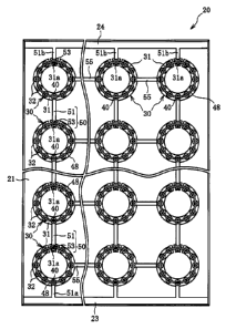
Fig. 6 is an elevation view of a first substrate on which a plurality of
clusters are arranged and wired in a matrix configuration having a plurality
of rows and a plurality of columns, with certain conductive members
removed;
Fig. 7 is an elevation view of the first substrate of Fig. 6 in its state
with the conductive members connected on each cluster;
Fig. 8 is a sectional view at VIII-VIII line of Fig. 2;
Fig. 9 is an sectional view at IX-IX line of Fig. 2;
Fig. 10 is a sectional view of a spherical solar cell;
Fig. 11 is an equivalent circuit diagram of the solar battery module;
Fig. 12 is an enlarged sectional view showing the behavior of light that
is incident onto the solar battery module, the essential portion of the solar
battery module;
Fig. 13 is an elevation view of a first substrate of a solar battery
8
CA 02731984 2011-01-25
module according to a second embodiment, on which a plurality of clusters
are arranged and wired in a snowflake configuration, with certain conductive
members removed;
Fig. 14 is an elevation view of the first substrate in its state with the
conductive members connected to each cluster of Fig. 13;
Fig. 15 is a sectional view at XV-XV line of Fig. 14;
Fig. 16 is a sectional view at XVI-XVI line of Fig. 14;
Fig. 17 is an enlarged elevation view of the essential portion of Fig. 14;
Fig. 18 is a sectional view at XVIII-XVIII line of Fig. 17;
Fig. 19 is an elevation view of a first substrate of a solar battery
module according to a third embodiment, on which a plurality of clusters are
arranged and wired in a bead curtain configuration;
Fig. 20 is a sectional view at XX-XX line of Fig. 19;
Fig. 21 is a sectional view at XXI-XXI line of Fig. 19;
Fig. 22 is an enlarged sectional view of the essential portion of the solar
cell of Fig. 20;
Fig. 23 is an enlarged elevation view of the essential portion of the
solar cell of Fig. 19;
Fig. 24 is an enlarged sectional view of the essential portion of a
conductive connecting piece and a bypass diode of Fig. 20;
Fig. 25 is an enlarged sectional view of the essential portion of a
conductive connecting piece and a bypass diode of Fig. 19;
Fig. 26 is a sectional view of a solar cell according to a fourth
embodiment;
Fig. 27 is an enlarged sectional view of the essential portion of the solar
cell; and
9
CA 02731984 2011-01-25
Fig. 28 is an equivalent circuit diagram of the solar cell.
DESCRIPTION OF NUMERALS
[0014)
1 solar battery panel
3 external surrounding frame
20, 20A, 20B see-through type solar battery module
21 first substrate
22, 22B second substrate
23 positive terminal
24 negative terminal
27 molding material
29, 29A, 29B ceramic layer
30, 30A, 30B cluster
31, 31A, 31B conductive layer
32, 32A, 32B, 32C solar cell
33 layer of spherical semiconductor
34 flat surface
35 diffused layer
36 pn junction
37 first electrode
38 second electrode
39 reflection prevention layer
40, 40A, 40B bypass diode
48, 48A, 48B conductive member
50, 50A, 50B conductive connection member
51, 51A, 51B elongated conductive layer portion
CA 02731984 2011-01-25
53, 53A, 53B conductive connecting piece
55, 55A conductive layer bridge
BEST MODE FOR IMPLEMENTING THE INVENTION
[0015] In the following, various preferred embodiments for implementation
of the present invention will be explained.
EMBODIMENT 1
[0016] First, a solar battery panel 1 to which the present invention is
applied will be explained.
As shown in Figs. 1 to 5, the solar battery panel 1 is made as a window
material, and is constructed from an external surrounding frame 3 and three
see-through type solar battery modules 20. The three see-through type solar
battery modules 20 (hereinafter referred to as "modules") are oriented with
their long sides horizontal, and are assembled into the external surrounding
frame 3 so that they all lie in the same plane and are arranged in a matrix
form having three rows and one column.
[0017] Sealing material 15 (for example, silicon resin) is charged into the
gaps between the modules 20 and the external surrounding frame 3 and into
the gaps between vertically adjacent modules, and this serves to prevent
ingress of rain or harmful gases into the interior. It should be understood
that it is not necessary for the number of the modules 20 to be limited to
three; it would also be possible to change the size of the external
surrounding
frame 3, and to arrange the plurality of modules 20 in a plurality of rows
and/or a plurality of columns and then to assemble them into the external
surrounding frame.
[0018] As shown in Figs. 1, 3 to 5, the external surrounding frame 3 is
made from aluminum, and is made from a pair of upper and lower horizontal
11
CA 02731984 2011-01-25
frame members 5a, 5b and a pair of left and right vertical frame members 6a,
6b. To the upper horizontal frame member 5a, there are provided a
conductive interior terminal 8a that extends along the longitudinal direction
of the horizontal frame member 5a, a pair of left and right output terminals
9a that are connected to the two end portions of this interior terminal 8a,
insulating members 11a that insulate these output terminals 9a from the
external surrounding frame 3, leaf springs 12 that bias the interior terminal
8a downwards, and a backup member 13a that backs up the module 20 from
above and moreover insulates the interior terminal 8a from the horizontal
frame member 5a.
[0019] And to the lower horizontal frame member 5b, there are provided a
conductive interior terminal 8b that extends along the longitudinal direction
of the horizontal frame member 5b, a pair of left and right output terminals
9b that are connected to the two end portions of this interior terminal 8b,
insulating members 11b that insulate these output terminals 9b from the
external surrounding frame 3, and a backup member 13b that backs up the
module 20 from below and moreover insulates the internal terminal 8b from
the horizontal frame member 5b. It should be understood that the raw
material from which the external surrounding frame 3 is made is not limited
to being aluminum; various other metallic materials could be employed.
[0020] The upper and lower output terminals 9a, 9b are long and narrow
thin plate shaped members made from metal, and their one end portions are
integrally connected to left and right end portions of both of the interior
terminals 8a, 8b, while their other end portions are projected outward from
the external surrounding frame 3 towards the rear side of the panel 1.
Along with the upper interior terminal 8a being pressed towards a
12
CA 02731984 2011-01-25
negative terminal 24 of the upper module 20 by the leaf springs 12, a positive
terminal 23 of the upper module 20 is pressed towards the negative terminal
24 of the intermediate module 20, and a positive terminal 23 of the
intermediate module 20 is pressed towards a negative terminal 24 of the
lower module 20, all these terminals thus being reliably electrically
connected together. Moreover, by the positive terminal 23 of the lower
module 20 being pressed towards the lower interior terminal 8b by the
weight of the module 20 itself, a reliable electrical connection is
established
therebetween. The electrical connections between neighboring modules 20
are established by the upper positive terminal 23 of the upper module 20
being pressed by the weight of the upper module 20 into contact with the
negative terminal 24 of the intermediate module 20, and by the positive
terminal 23 of the intermediate module being also pressed into contact with
the negative terminal 24 of the lower module 20.
[0021] Next, only one of the see-through type solar battery modules 20 will
be explained, although three modules 20 are provided, since these three
modules 20 all have similar constructions.
As shown in Figs. 6 to 10, this module 20 generates electricity with a
plurality of spherical solar cells 32, and comprises an optically transparent
first substrate 21, a plurality of annular clusters 30 arranged on this first
substrate 21 in a matrix form having a plurality of rows and a plurality of
columns, an optically transparent second substrate 22 that is disposed
parallel to the first substrate 21 with the plurality of solar cells 32
sandwiched between them, and an optically transparent synthetic resin
molding material 27 that is charged between the substrates 21, 22 and is
molded into a state in which the plurality of clusters 30 are embedded
13
CA 02731984 2011-01-25
therein.
[0022] Next, the first substrate 21 and the second substrate 22 will be
explained. The first substrate 21 is made of a transparent glass plate with
the borders chamfered, and may, for example, be processed so that its
thickness is 2.8 mm, its height is 210 mm, and its width is 297 mm. The
positive terminal 23 (a positive side busbar) is provided at the lower edge
portion of the first substrate 21, and has a reversed letter-L cross-sectional
shape for external connection, and the negative terminal 24 (a negative side
busbar) is provided at the upper edge portion of the first substrate 21, and
has a letter-L cross-sectional shape for external connection (refer to Fig.
8).
And, similarly to the first substrate 21, the second substrate 22 is made from
transparent glass with the borders chamfered, and may, for example, be
processed so that its thickness is 2.8 mm, its height is 210 mm, and its width
is 297 mm. For the synthetic resin molding material 27 that is charged into
the gap between the substrates 21, 22, for example, EVA (ethylene vinyl
acetate) resin may be used.
[0023] Since the optically transparent synthetic resin molding material 27
is molded and solidified into a state in which the plurality of solar cells
32, a
plurality of conductive layers 31, a plurality of bypass diodes 40, and a
plurality of conductive connection members 50 all loaded between the
substrates 21, 22 are embedded therein. Accordingly it is possible to protect
the solar cells 32 and also to strengthen them against vibration and
mechanical shock, and moreover it is possible to prevent damage to the
module 20 as a whole, so that the safety can be enhanced. Moreover, even if
exceptionally the solar cell 32 suffers damage, the broken shards are
prevented from flying off or coming away as well as laminated glass which is
14
CA 02731984 2011-01-25
normally used and wired glass,
[0024] Now the method for manufacturing this module 20 will be explained
in a simple manner. The plurality of clusters 30 are all arranged on the first
substrate 21, and then the molding material 27 in sheet form is laid over the
plurality of clusters 30, and the second substrate 22 is superimposed
thereupon, with the whole being received in a laminator device of a per se
known type. This laminator device has a vacuum chamber that is divided
horizontally by an elastic membrane. A heater is provided underneath and
applies heat to the workpiece via a plate. The workpiece with the second
substrate 22 laid over it is placed on the heat application plate, and, while
gas is exhausted from the spaces that are horizontally partitioned by the
membrane, heat is applied to the molding material 27 to a temperature of
around 150 C so that it becomes melted.
[0025] Then, as air is admitted into only the evacuated vacuum chamber
above the membrane, the substrates 21, 22 are pressurized from both their
sides by the pressure of this admitted air, due to the membrane. And the
molding material 27 (i.e. EVA resin) is cooled and solidifies while being held
in this state. Due to this thermal melting and solidification the molding
material 27, which was a milky white color, becomes transparent, and the
plurality of clusters 30 are adhered between the substrates 21, 22, and are
sandwiched on both sides by the glass substrates 21, 22 so that an integrated
module 20 is completed.
[0026] Next, the construction of the clusters 30 will be explained.
Since all of the plurality of clusters 30 have the same structure, only a
single cluster 30 will be explained. As shown in Figs. 2, 6 to 10, the cluster
30
is formed as annular, and comprises a conductive layer 31 that is formed on
CA 02731984 2011-01-25
the first substrate 21, ten solar cells 32, a bypass diode 40, a conductive
connecting piece 53 of a conductive connection member 50, and a conductive
member 48 that electrically connects together these solar cells 32, the bypass
diode 40, and the conductive connecting piece 53.
[0027] Next, the conductive layer 31 will be explained.
The conductive layer 31 is formed in an annulus on the inner surface of
the first substrate 21, and positive electrodes 37 of the ten solar cells 32,
a
negative electrode 45 of the bypass diode 40, and the conductive connecting
piece 53 are arranged thereupon at regular intervals and are connected
thereto by electrically conductive paste 31b. The bypass diode 40 and the
conductive connecting piece 53 are arranged between the ten solar cells 32 so
as mutually to oppose one another, with a separate conductive layer portion
31a to which the conductive connecting piece 53 is connected being
electrically isolated by two slits. This separate conductive layer portion 31a
is formed integrally with an elongated conductive layer portion 51 of the
conductive connection member 50. It should be understood that the
proportion of occupied in the entire area by a light transmission region in
which sunlight is not intercepted by the conductive layers 31 is greater than
or equal to 50%.
[0028] For this conductive layer 31, first, as the foundation for the
conductive layer 31, a ceramic paste into which a pigment of a preferred color
has been mixed is silk screen printed on the first substrate 21 and is fired,
so
that a ceramic layer 29 is formed. Next, a silver paste including glass frit
is
printed on the ceramic layer 29 by a silk screen process, and is fired at 550
to
620 C so as to form the conductive layer 31. The width of this conductive
layer 31 is approximately 2.4 mm, so that it is larger than the diameter of
16
CA 02731984 2011-01-25
the solar cells 32. It would be acceptable for the thickness to be about
0.25 mm, and, according to the conditions of use, the thickness may be in the
range of from 0.01 mm to 0.5 mm. It should be understood that elongated
conductive layer portions 51, 51a, and 51b of a conductive connection
member 50 and a conductive layer bridge 55 that will be described later are
also formed at the same time as the conductive layer 31.
[0029] Next, the structure of the spherical solar cells 32 will be explained.
As shown in Fig. 10, a solar cell 32 is mounted with its conducting
direction perpendicular to the first substrate 31, and incorporates a
spherical
p type semiconductor 33, a flat surface 34 that is formed by grinding a
portion of the surface of the spherical semiconductor 33, a pn junction 36
shaped as a spherical surface that is defined by an n type diffused layer 35
being formed on the surface layer portion of the spherical semiconductor 33,
a pair of positive and negative electrodes 37, 38 (first and second
electrodes)
that are electrically connected to both ends (both sides) of the pn junction
36
and are formed so as to oppose one another with the center of the spherical
semiconductor 33 interposed between them, and a reflection prevention layer
39 that is formed on the entire surface except for the positive and negative
electrodes 37, 38. This positive electrode 37 is electrically connected on the
conductive surface layer 31 with conductive paste 31b, while the negative
electrode 38 is electrically connected to the conductive member 48 with
conductive paste 48a.
[0030] The method for manufacture of this solar cell 32 will now be
explained in a simple manner.
This solar cell 32 is made by a technique of, for example, letting a
liquid drop of silicon fall freely so as to solidify partway down into a
spherical
17
CA 02731984 2011-01-25
p type single silicon crystal 33 of diameter approximately 1.6 mm, and by
then grinding a portion of its surface to provide the flat surface 34. Then
the
spherical surface shaped pn junction 36 is created by forming the n type
diffused layer 35 by diffusing an n type impurity to a depth of about 0.1 Jim
inward from the surface, except for the flat surface 34 and a portion of its
periphery. It should be understood that it would also be acceptable to create
a pn junction by forming a p type diffused layer on a spherical n type single
silicon crystal.
[0031] Furthermore after forming, as a reflection prevention layer 39, a
silicon oxide (SiO2) layer (or, a layer of silicon nitride (SiN)) over the
entire
spherical surface including the flat surface 34, next a paste including silver
is printed in the form of dots on the reflection prevention layer 39, at the
apex portions of the flat surface 34 and of the spherical surface. Then, when
heat is applied in a gaseous atmosphere up to around 800 C, the silver paste
pierces through the reflection prevention layer 39 and contacts against the p
type flat surface 34 and the surface of the n type diffused layer 35 with low
resistance, and thereby the positive electrode 37 and the negative electrode
38 are provided and the solar cell 32 is completed.
[0032] According to this solar cell 32, since as shown in Fig. 10 the pn
junction 36 is provided so as to have a spherical surface, accordingly, with
the exception of the flat surface 34 and the electrodes 37, 38, the cross
sectional area for light reception is always constant irrespective of the
angle
of incidence of the sunlight, so that a stable output is obtained.
Furthermore,
since the electrodes 37, 38 are provided as centered on the p type and n type
surfaces with the center of the sphere interposed between them, accordingly
the sum of the distances connecting from the electrodes 37, 38 to any points
18
CA 02731984 2011-01-25
a, b, or c on the pn junction 36 is equal, so that the distances through which
carriers generated by absorption at the points a, b, or c shift are equal, and
the distribution of the flow of electrical current becomes almost equal and
the curve fill factor becomes large. Moreover, since the range for light
reception is three dimensional and the light other than direct solar
illumination, in other words the reflected light and the diffused light, are
both received simultaneously, accordingly the level of utilization of
peripheral light is also high, so that high output is obtained.
[0033] Next, the bypass diode 40 will be explained.
As shown in Fig. 8, the bypass diode 40 is fixed on the first substrate 21
so that its conductive direction lies in the direction orthogonal to the first
substrate 21, and is electrically connected to the conductive layers 31 and
the
conductive member 48 in inverse parallel to the ten solar cells 32. This
bypass diode 40 is a circular cylinder and has a height similar to that of the
solar cells 32, and is made by forming a pn junction 43 by diffusing a p type
impurity into a semiconductor 41, thus making a p type diffused layer 42,
and then contacting a negative electrode 45 against the surface of the n type
semiconductor 41 and a positive electrode 46 against the surface of the p type
diffused layer 42, both with low resistance.
[0034] Due to this bypass diode 40, if the ten solar cells 32 within one
cluster 30 that are all connected in inverse parallel with the diode 40 are
shielded from light so that their functioning stops, even though voltage in
the opposite direction originating in the solar cells 32 within the other
clusters 30 that are functioning normally (i.e. to generate electricity) is
applied to these solar cells 32 in this cluster 30 whose function has stopped,
due to this bypass diode 40 bypassing the current, it is possible for the
solar
19
CA 02731984 2011-01-25
cells 32 that are connected in inverse parallel to be protected from
destruction or damage, and it is possible to keep the decrease in the output
of
the entire module 20 due to the shielding from light of a portion including
the cluster 30 down to a minimum.
[0035] Next, the conductive member 48 will be explained.
As shown in Figs. 7 to 9, the conductive member 48 is a metallic wire of
diameter, for example, 0.3 mm made from copper alloy plated with silver and
formed into an annulus, and it is electrically connected with conductive paste
48a to the negative electrodes 38 of the ten solar cells 32, to the positive
electrode 46 of the bypass diode 40, and to the conductive connecting piece
53. Via the conductive member 48 and the conductive layer 31, the ten solar
cells 32 and the conductive connecting piece 53 are electrically connected in
parallel, and the bypass diode 40 is electrically connected to the first
substrate 31 and the conductive member 48 in inverse parallel relative to the
ten solar cells 32, whereby one of the annular clusters 30 is formed.
[0036] Next, a conducting construction by which the plurality of clusters 30
are electrically connected together will be explained.
As shown in Figs. 6, 7, the plurality of clusters 30 are laid out in a
matrix form having a plurality of rows and a plurality of columns. The
conductive layer 31 of each of the plurality of clusters 30 in each column is
electrically connected to the conductive member 48 of the lower side adjacent
cluster 30 via the conductive connection member 50. The plurality of
conductive layers 31 in the plurality of clusters 30 in each row are
electically
connected in parallel by conductive layer bridges 55. In other words, among
the plurality of clusters 30, the plurality of solar cells 32 of the plurality
of
cluster groups of each column are connected in series via the conductive
CA 02731984 2011-01-25
connection members 50, and the plurality of solar cells 32 of the plurality of
cluster groups of each row are connected in parallel via the conductive layer
bridges 55.
[0037] The conductive connection member 50 includes a rectilinear
elongated conductive layer portion 51 elongated from the conductive layers
31 and the conductive connecting piece 53 connected to the elongated
conductive layer portions 51. The conductive connecting piece 53 constitutes
a portion of the cluster 30. The elongated conductive layer portion 51 is made
from silver paste as well as the conductive layers 31. The conductive
connecting piece 53 is a circular cylindrical piece made from metal, and has
similar diameter and height to the bypass diode 40. It should be understood
that the elongated conductive surface layer portion 51 need not necessarily
be rectilinear; it would be acceptable, according to the design, to form to be
shaped as zigzags or as curved lines.
[0038] The conductive layer bridges 55 are provided so as electrically to
connect the plurality of conductive layers 31 of each row. These conductive
layer bridges 55 are made from silver paste as well as the conductive layers
31. It should be understood that the conductive layer bridges 55 need not
necessarily be rectilinear; it would be acceptable for them to be shaped as
zigzags or as curved lines. The conductive layer 31 of the lowermost cluster
of each column is connected to the positive terminal 23 via an elongated
conductive layer portion 51a, and the separate conductive layer portion 31a
of the conductive layer 31 of the uppermost cluster 30 is connected to the
negative terminal 24 via an elongated conductive layer portion 51b.
25 [0039] Since the plurality of clusters 30 are connected in series-parallel
in
this manner, even if some of the clusters 30 have stopped functioning, there
21
CA 02731984 2011-01-25
is no stopping or decrease of the electricity generation effectiveness of
those
other clusters 30 that still remain normal, since electrical current still
flows
through the other clusters by detouring past those clusters 30 whose
functioning has stopped, so that it is possible to reduce to a minimum the
influence that is exerted to decrease the output of this entire module 20.
[0040] Next, an equivalent circuit diagram for this module 20 will be
explained. Fig. 11 is a drawing showing an equivalent circuit of this module
20 that has a plurality of clusters 30 arranged in a matrix configuration
having a plurality of rows and a plurality of columns. However, the row
direction is vertical and the column direction is horizontal in Fig. 11.
Here, as an example, the output will be explained of a module in which
a plurality of clusters 30 are installed arranged in four rows and three
columns. If the open circuit voltage of one solar cell 32 is, for example, 0.6
V,
then a voltage of 2.4 V will be generated, since four clusters 30 are
connected
in series between the positive terminal 23 and the negative terminal 24.
And, if the electrical current generated by one solar cell 32 of each cluster
of
each row is termed I, then 30xI of electrical current will flow from the
positive terminal 23, since three clusters 30 in each row are connected in
parallel.
[0041] In other words, with the solar battery panel 1 to which three of the
modules 20 are assembled, a voltage of 7.2 V is generated, and a current of
30xI flows out from the output terminal 9b. It should be understood that it is
possible to implement increase of the output voltage of the module 20 by
increasing the number of clusters 30 that are connected in series, while,
when the output current of the module 20 is to be increased, the number of
clusters 30 connected in parallel should be increased. In the same way with
22
CA 02731984 2011-01-25
the panel 1 as well, if the output voltage is to be increased, then this can
be
done by increasing the number of modules 20 that are connected in series;
whereas, if the output current from the modules 20 is to be increased, then
this can be done by increasing the number of modules 20 that are connected
in parallel.
[0042] Next, the behavior of light incident on this module 20 will be
explained. Fig. 12 is an enlarged view of a portion of this module 20, for
showing the behavior of light incident thereupon. The incident light beams a
are light beams that pass through from the second substrate 22 to the first
substrate 21, and the incident light beams b are light beams that are directly
incident from the second substrate 22 on the solar cell 32, while the incident
light beams b' are light beams from the incident beams b that are reflected
back by the second substrate 22.
[0043] The incident light beams c are light beams that are incident from
the second substrate 22 and are reflected by the conductive layers 31 around
the solar cells 32 to then be incident on the solar cells 32, the incident
light
beams d are light beams that are multiply reflected by portions other than
the surroundings of the solar cells 32 and are then incident on the solar
cells
32, the incident light beams e are beams that pass from the first substrate 21
through the second substrate 22, the incident light beams f are beams that
are incident from the first substrate 21 and are reflected by the second
substrate 22 to be incident on the solar cells 32, and the incident light
beams
f are reflected light from the incident light beams f that are reflected by
the
first substrate 21. In other words, except for the light that passes through
the substrates 21, 22 in order to provide indoor lighting (i.e. the
transmitted
sunlight) which is of course the light that is incident vertically on the
23
CA 02731984 2011-01-25
substrates 21, 22, the light that is incident in very many other directions
can
easily be conducted to the solar cells 32, so that it is possible to enhance
the
efficiency of utilization of the incident light.
[0044] In this manner, with this plurality of solar cells 32, it is possible
to
absorb light that is incident from many directions due to reflection and
scattering between the substrates 21, 22, with the exception of the light that
is directly incident. In particular, since the conductive layers 31 have high
electrical conductivity and high optical reflectivity since they utilize
silver,
the amount of light that arrives at the solar cells 32 due to internal
reflection
is increased while the electrical resistance losses due to the wiring are
small,
so that there is the technical advantages of enhancement of the
photoelectromotive force. Moreover, since the solar cells 32 in these clusters
30 are arranged at regular intervals from the centers of circles in a radial
manner, accordingly it is possible to minimize the directional dependence of
the output of the module 20 on the rotational orientation of its light
reception
surface around the vertical axis and on the angle of incidence.
[0045] Next, the advantages obtained by this see-through type solar
battery module 20 will be explained.
According to this module 20, it is possible for light that has been
absorbed by the plurality of solar cells 32 to generate electricity, while
light
which has passed through between the plurality of solar cells 32
(transmitted sunlight) to light the indoors. The ratio of the amount of light
that generates electricity to the amount of light that passes through for
illumination depends on the projected area of all of the solar cells 3
installed
on the first substrate 21. In other words, if it is desired to moderate strong
sunlight, then the projected area of all of the solar cells 32 is increased
24
CA 02731984 2011-01-25
according to the density at which the solar cells 32 are arranged, so that it
is
possible to increase the amount of electricity that is generated.
[0046] According to this module 20, since it is possible to set the pattern in
which the plurality of clusters 30 are arranged freely, it is possible to
provide
the plurality of clusters 30 in patterns of various types, so that the freedom
of design becomes high. Moreover, it is also possible to silk screen print a
ceramic paste to which pigment of an appropriate color has been added on
the surface of the first substrate as a foundation for the above described
conductive layers 31, and then to fire this paste to form the ceramic layers
29, thus creating a beautiful and colorful pattern when seen from the inside
of the substrate 21 (i.e. from its indoor side). Furthermore, it is possible
to
make it difficult to see the solar cells 32 or the conductive layers 31 due to
the ceramic layers 29. Because of this, it is possible to implement a module
whose freedom of design when used as a building material or window
material is high, quite apart from its function for optical electricity
generation. Moreover, by forming the ceramic layers 29, along with
enhancing the adherence to the conductive layers 31, it is also possible to
enhance the strength of the glass substrate 21.
[0047] According to this module 20, not only are the annular clusters 30
arranged in a matrix configuration that has a plurality of rows and a
plurality of columns expressing a geometric design, but also it can be taken
advantage of as a window material that can reconcile the needs for
generation of electricity from sunlight and also for lighting (i.e. for
transmission of sunlight), and the internal diameters and the external
diameters of the annular clusters 30 and the gaps between these clusters 30
can be designed in consideration of freedom of design, optical transmittivity,
CA 02731984 2011-01-25
and photoelectric output.
[0048] According to this module 20, the wiring provided by the conductive
layers 31 and the conductive connection members 50 and the conductive
layer bridges 55 has an appropriate width capable of hiding the solar cells 32
as seen from the orthogonal direction to the conductive layer 31, and this is
done in order for it to be possible to accentuate the pattern or design of the
wiring, so that, along with making it possible to enhance the freedom of
design as seen from the rear side of the module 20, it is also possible to
increase the amount of the light incident from the front surface that is
reflected and received by the solar cells 32, so that the output is enhanced.
[0049] According to this module 20, when the sizes of the plurality of solar
cells 32 and of the plurality of conductive layers 31 are compared with those
of a prior art flat plate type solar cell or a thin layer solar cell, since
they are
smaller and thinner and also can be arranged in a dispersed configuration,
accordingly they do not themselves constitute any hindrance to their own
wide field of view, and thus they can be utilized for manufacturing a
see-through type solar battery module through which both interior views and
exterior scenery can be viewed with uniform lighting (i.e. sunlight
transmission) performance and no sense of discomfort.
[0050] According to this module 20, by embedding the plurality of solar
cells 32 between the optically transparent substrates 21, 22, and by using
this module 20 for a window material, it is possible to reduce the total costs
in comparison with a case in which electricity is generated using an
independent solar battery panel, in which costs are entailed by the cost of
materials such as glass or the like, and also for installation. Moreover,
since
the components such as the plurality of spherical solar cells 32 and the
26
CA 02731984 2011-01-25
plurality of conductive layers 31 are first arranged, and then the second
substrate 22 is laid over them, accordingly it is not necessary to arrange any
components on the second substrate 22, so that the assembly process is easy.
EMBODIMENT 2
[0051] In this second embodiment, an example is disclosed of a see-through
type solar battery module 20A in which the pattern of arrangement of the
plurality of spherical solar cells in the plurality of clusters 30 of the
first
embodiment is changed; and only the structures which are different from
those of the first embodiment will be explained.
As shown in Figs. 13 to 18, these clusters 30A are formed like
snowflakes, and each comprises a conductive surface layer 31A formed on
the first substrate 21, eleven solar cells 32A, a bypass diode 40A, a
conductive connection member 50A, and a conductive member 48A that
electrically connects these solar cells 32A, the bypass diode 40A, and the
conductive connecting piece 53A. It should be understood that the snowflake
configuration in which the cluster 30A is formed is a pattern that includes an
inner hexagon shape and an outer hexagon shape that is positioned
concentrically on the outside of the inner hexagon shape, and in which the
center of the cluster, the six vertices of the inner hexagon shape, and the
six
vertices of the outer hexagon shape are connected with six radially extending
straight lines.
[0052] On the first substrate 21, the conductive layer 31A comprises 13
dot-shaped conductive layers 61 that are arranged at the center point, the
vertices of the inner hexagon shape, and the vertices of the outer hexagon
shape, and linear conductive layers 62 that join the dot-shaped conductive
layers 61 from the center of the cluster 30A towards its outside. These
27
CA 02731984 2011-01-25
dot-shaped conductive surface layers 61 are formed to be of diameter larger
than the diameter of the solar cell 32. Among the linear conductive surface
layers 62, that linear layer 62 between the dot-shaped conductive layer 61 on
which the conductive connecting piece 53A is positioned and the dot-shaped
conductive layer 61 on which the adjacent solar cell 32A in the center
direction is connected is omitted. This detached dot-shaped conductive
surface layer 62 is formed integrally with one end portion of the elongated
conductive layer portion 51A.
[0053] The plurality of solar cells 32A in a cluster 32A include six solar
cells 32A that are arranged on the dot-shaped conductive layers 61 at the
vertices of the inner hexagon shape and five solar cells 32A that are
arranged on the dot-shaped conductive surface layers at vertices of the outer
hexagon shape. The bypass diode 40A is positioned on the dot-shaped
conductive layer 61 at the central portion of the inner hexagon shape. In
other words, the eleven solar cells 32A are connected in parallel, and the
bypass diode 40A is connected in inverse parallel with these solar cells 32A.
The conductive member 48A is formed in a snowflake configuration so as to
correspond to the conductive layers 31A, and the negative electrodes 38 of
the solar cells 32A, the positive electrode 46 of the bypass diode 40A, and
the
conductive connecting piece 53A are electrically connected together via this
conductive member 48A.
[0054] Next, a conducting construction that electrically connects together
the plurality of clusters 30A will be explained.
As shown in Figs. 13, 14, the plurality of clusters 30A are arranged in a
plurality of rows and a plurality of columns so that the central portions of
their inner hexagon shapes are positioned on the mesh points of a mesh of
28
CA 02731984 2011-01-25
equilateral triangles. The conductive layer 31A of each of the plurality of
clusters 30A in each column is electrically connected to the conductive
member 48A of the lower side adjacent cluster 30A via the conductive
connection member 50A.
The plurality of conductive layers 31A of the plurality of clusters 30A
arranged along each zigzag row in the direction orthogonal to the column
direction being electrically connected in parallel by the conductive layer
bridges 55A. The conductive connection member 50A has an elongated
conductive layer portion 51A electrically connected to the conductive layer
31A, and a conductive connecting piece 53A that is electrically connected to
the one end portion of the elongated conductive layer portion 51A, and the
conductive connecting piece 53A is located on a vertex of the outer hexagon
shape. The conductive connecting piece 53A is shaped as a sphere made from
metal.
[0055] Next, the advantages of this module 20A will be explained.
According to this module 20A, since 11 solar cells 32A are arranged as
radially extending from the center of the cluster 30A with gaps of 60
between them, accordingly the direction dependence of the output with
respect to the light that is incident on the module 20A becomes lower, as
compared with the above first embodiment.
Since the clusters 30A along the row direction are arranged in a zigzag
configuration, it is possible to reduce the occurrence of the situation in
which
all of the solar cells 32A that are connected in the same parallel row stop
functioning due to a linear shadow, so that solar cells 32A may be provided
instead of the bypass diodes 40A, so that it is possible to enhance the output
of the module 20A. From the front surface or the rear surface of this module
29
CA 02731984 2011-01-25
20A, a pattern like that of a snowflake configuration is seen due to the
conductive layers 31A and the conductive members 48A, and this has high
freedom of design, and can be employed for a solar battery panel 1 that
absorbs light coming from outside that includes sunlight, and that generates
electricity with good efficiency. It should be understood that explanation of
the other advantages of this embodiment is omitted, since they are the same
as in the case of the first embodiment.
EMBODIMENT 3
[0056] In this third embodiment, an example is disclosed of a see-through
type solar battery module 20B in which the pattern of arrangement of the
plurality of spherical solar cells in the plurality of clusters 30 of the
first
embodiment is changed; and only the structures which are different from
those of the first embodiment will be explained.
As shown in Figs. 19 to 25, these clusters 30B are formed as straight
lines extending in the horizontal direction, and one of them comprises a
conductive layer 31B formed on the inner surface of the first substrate 21, a
plurality of spherical solar cells 32B, a bypass diode 40B, a conductive
connecting piece 53B of the conductive connection member 50B, and a
conductive member 48B that connects these solar cells 32B, the bypass diode
40B, and the conductive connecting piece 53B together.
[0057] The conductive layer 31B is a single straight line, and comprises a
plurality of conductive circular layers 64 that correspond to the plurality of
solar cells 32B, two square shaped conductive layers 65 that are provided at
both end sides of these conductive circular layers 64, and a linear conductive
layer 66 that connects together the square shaped conductive layers 65 to the
conductive circular layers 64 and also between the conductive circular
CA 02731984 2011-01-25
layers 64, except not between the square shaped conductive layer 65 to which
the conductive connecting piece 53B is connected and the adjacent
conductive circular layer 64. A plurality of these conductive layers 31B are
formed on the first substrate 21, mutually parallel and spaced apart at
constant intervals along the vertical direction. It should be understood that
the peripheral portion 22a of the inner side of the second substrate 22B is
made as frosted glass by roughening its surface by a sandblasting process,
and thus is put into a state in which the positive terminal 23 and the
negative terminal 24, and the bypass diodes 40B and the conductive
connecting pieces 53B, are hard to see from the front surface of the module
20B.
[0058] With regard to the plurality of solar cells 32B in each of the clusters
30B, the positive electrodes 37 of the solar cells 32B that are arranged in
one
straight line are connected on the conductive circular layers 64, and on the
one hand the conductive connecting piece 53B is arranged so as to be
electrically isolated from the conductive circular layer 64 that corresponds
to
the square shaped conductive layer 65, while on the other hand the bypass
diode 40B is connected so as to be connected in inverse parallel with the
solar
cells 32B. The conductive member 48B is formed as a single straight line,
and the solar cells 32B, the bypass diode 40B, and the conductive connecting
piece 53B are electrically connected together via this conductive member
48B.
[0059] Next, a conducting construction that electrically connects together
the plurality of clusters 30B will be explained.
This plurality of clusters 30B are connected in series from top to
bottom via the conductive connection members 50B. The square shaped
31
CA 02731984 2011-01-25
conductive surface layer 65 on the right side of the uppermost cluster 30B is
connected to the negative terminal 24 via an elongated conductive layer
portion 51bB, while the square shaped conductive layer 65 on the right side
of the lowermost cluster 30B is connected to the positive terminal 23 via an
elongated conductive layer portion 51aB.
[0060] Next, the advantages of this module 20B will be explained.
With this module 20B, the conductive layers 31B that extend in single
straight lines and to which the solar cells 32B are adhered so that the light
can pass through are formed so as to be spaced at certain intervals, and
accordingly it is possible to determine the sunlight transmission ratio during
use as a window material, according to the area of the portion that light can
pass through, other than these conductive layers 31B. The pattern created
by the conductive layers 31B and the conductive members 48B, in which
there is freedom of design, can be seen from the front surface or from the
rear
surface and moreover it can be utilized for a solar battery panel 1 that
absorbs light from the exterior, including sunlight, with good efficiency and
generates electricity. It should be understood that explanation of the other
advantages of this embodiment is omitted, since they are the same as in the
case of the first embodiment.
EMBODIMENT 4
[0061] In this fourth embodiment, instead of the spherical solar cells 32,
32A, and 32B of the first through the third embodiment, solar cells 32C of
this embodiment may be used. Moreover, in this case, it is possible to replace
the bypass diodes with solar cells 32B. As shown in Figs. 26 to 28, one of
these solar cells 32C comprises a spherical p type single silicon crystal 71,
a
flat surface 72 formed at one end portion of the single silicon crystal 71, an
n+
32
CA 02731984 2011-01-25
diffused layer 73 formed on the surface portion of the single silicon crystal
71
with the exception of this flat surface 72, a positive electrode 75 and a
negative electrode 76 that oppose one another with the center of the single
silicon crystal 71 interposed between them, a p+ diffused layer 77 that is
formed on an outer surface portion of the flat surface 72 of the single
silicon
crystal 71 on its side towards the positive electrode 75, and a reflection
prevention layer 78 that covers over the surface of the solar cell 32C, with
the exception of its portions where the positive electrode 75 and the negative
electrode 76 are provided.
[0062] A pn+ junction 74 is formed at the surface portion of the single
silicon crystal 71, and this functions as a pn junction that is capable of
generating photoelectromotive force; and this pn+ junction 74 is formed as a
spherical surface that is positioned at a substantially constant depth from
the surface of the single silicon crystal 71, except for the flat surface 72.
The
pair of electrodes 75, 76 are connected at spots to both ends of the pn+
junction 74. And a p+n+ junction 79 that has a backward diode characteristic
due to a tunnel effect is formed in an annulus on the portion towards the
single silicon crystal 71 external to and around the positive electrode 75. In
other words, the equivalent circuit for this solar cell 32C is as shown in
Fig.
28.
[0063] According to this module, even if some or all of the solar cells 32C of
the clusters of one of the plurality of rows of clusters that are connected in
parallel enter into a shadow so that reverse voltage is applied to these solar
cells 32C, a bypass electrical current flows via the p+n+ junctions 79 of the
solar cells 32C in this row (refer to Fig. 28). Accordingly, even if a shadow
falls in any type of pattern on the module in which the plurality of clusters
33
CA 02731984 2011-01-25
are electrically connected in a series-parallel circuit in a mesh pattern,
there
is no loss of generated electrical power, it becomes possible to take it out,
and
no bad influence is exerted on each of the solar cells. Furthermore, since no
bypass diodes are provided, it is possible to increase the number of the solar
cells, and thereby to enhance the output of the module.
[0064] Next, certain variant embodiments in which the above embodiment
is somewhat altered will be explained.
[1] Since the proportion between the output electrical power of this
module and its sunlight transmission ratio (or light shielding ratio) depends
principally on the output electrical power of the plurality of solar cells
that
are used and the number thereof that are used, and on the total area
shielded from the light by the plurality of conductive layers that are
provided
on the optically transparent first substrate, accordingly various designs are
possible for the arrangement of the plurality of solar cells and the number
thereof that are used, corresponding to the pattern or design of the
conductive layers on the first substrate, in order further to enhance the high
added value and the freedom of design for use as a window material.
[2] Apart from application in the above see-through type solar battery
panel, this module can also be applied as a constructional material including
a window material that it is desired to use, such as, for example, a glass
window, an atrium, a top light, a curtain wall, a facade, a canopy, a louver,
a
double-skin outer surface, a balustrade for a balcony, a soundproofing wall
for a high speed road or railroad, or the like.
INDUSTRIAL APPLICABILITY
[0065] With this see-through type solar battery module, by providing the
plurality of clusters that include the plurality of spherical solar cells, by
34
CA 02731984 2011-01-25
configuring these clusters in annular or snowflake configurations or in
straight lines, and by arranging the plurality of clusters, it is possible to
enhance the permitted scope for selection of the ratio between the sunlight
transmission ratio and the electrical generation capability, so that it is
possible to obtain higher freedom of design in use as a window material.