Note: Descriptions are shown in the official language in which they were submitted.
CA 02732189 2016-01-05
W02010/015315 1 PCT/EP2009/005144
Contactless loop probe
The present invention relates to a contactless loop
probe for the contactless coupling-out of an RE signal for
a contactless measuring system, having at least one
coupling structure and at least one first signal conductor
or guide which is electrically connected to the coupling
structure by a first transition and which is electrically
connected by a second transition to an output for
electrical connection to the measuring system.
The use of contactless loop measuring probes for
detecting interfering emissions is known, particularly in
the field of electromagnetic compatibility (EMC), from for
example H. Whiteside, R. W. P. King "The loop antenna as a
probe", IEEE Transactions on Antennas and Propagation, Vol.
12, No. 3, pp. 291-297, May 1964, or M. Kanda, "An
electromagnetic near-field sensor for simultaneous electric
and magnetic-field measurements", IEEE Transactions on
Electromagnetic Compatibility, Vol. 26, No. 3, pp. 102-110,
August 1984, or M. E. G. Upton, A. C. Marvin, "Improvements
to an electromagnetic near-field sensor for simultaneous
electric and magnetic field measurements", IEEE
Transactions on Electromagnetic Compatibility, Vol. 35, No.
1, pp. 96-98, February 1993.
It is also known for loop probes to be used in the
production of directional couplers from, for example, K. W.
Wagner "Induktionswirkung von Wanderwellen in
Nachbarleitungen" [Inductive effect of travelling waves on
neighbouring lines], Elektronische Zeitschrift, Vol. 35,
pp. 639-643, 677-680, 705-708, 1914; P. P. Lombardini, R.
F. Schwartz, P. J. Kelly, "Criteria for the design of loop-
type directional couplers for the L band", IEEE
CA 02732189 2011-01-27
W02010/015315 2 PCT/EP2009/005144
Transactions on Microwave Theory and Techniques, Vol. 4,
No. 4, pp. 234-239, October 1956; B. Maher, "An L-band
loop-type coupler", IEEE Transactions on Microwave Theory
and Techniques", Vol. 9, No. 4, pp. 362-363, July 1961; F.
De Groote, J. Verspecht, C. Tsironis, D. Barataud and J.-P.
Teyssier, "An improved coupling method for time domain
load-pull measurements", European Microwave Conference,
Vol. 1, p. 4 et seq. October 2005 or K. Yhland, J.
Stenarson, "Noncontacting measurement of power in
microstrip circuits", in 65" ARFTG, pp. 201-205, June 2006.
A directional coupler is a four-port device which generally
comprises two lines which are coupled to one another. The
job of the directional coupler is to separate the forward
and backward waves on a line.
Rather than loop probes, what are also used in EMC
technology and for characterising electrical components are
purely inductive or capacitive probes, as is known for
example from T. Zelder, H. Eul, "Contactless network
analysis with improved dynamic range using diversity
calibration", Proceedings of the 36th European Microwave
Conference, Manchester, UK, pp. 478-481, September 2006; T.
Zelder, H. Rabe, H. Eul, "Contactless electromagnetic
measuring system using conventional calibration algorithms
to determine scattering parameters", Advances in Radio
Sciences - Kleinheubacher Berichte 2006, Vol. 5, 2007; T.
Zelder, I. Rolfes, H. Eul, "Contactless vector network
analysis using diversity calibration with capacitive and
inductive coupled sources", Advances in Radio Science -
Kleinheubacher Berichte, Vol. 5, 2007, or J. Stenarson, K.
Yhland, C. Wingqvist, "An in-circuit noncontacting
measurement method for S-parameters and power in planar
circuits", IEEE Transactions on Microwave Theory and
Techniques, Vol. 49, No. 12, pp. 2567-2572, December 2001.
CA 02732189 2011-01-27
W02010/015315 3 PCT/EP2009/005144
A possible coupling structure for separating forward
and backward waves is the loop-type directional coupler,
which was described by P. P. Lombardini, R. F. Schwartz, P.
J. Kelly in "Criteria for the design of loop-type
s directional couplers for the L band", IEEE Transactions on
Microwave Theory and Techniques, Vol. 4, No. 4, pp. 234-
239, October 1956 and by B. Maher in "An L-band loop-type
coupler" IEEE Transactions on Microwave Theory and
Techniques, Vol. 9, No. 4, pp. 362-363, July 1961. A loop-
type directional coupler comprises a loop of conductor or
guide which is positioned above or in a waveguide.
Waveguides of any desired kinds may be used in this case
such as hollow waveguides, planar strip lines, or co-axial
lines. There are a variety of uses for a loop-type
is directional coupler. F. De Groote et al (op. cit) for
example used a loop-type directional coupler as a component
of a contactless measuring system in 2005 and Yhland et al
(op. cit.) used one as a component of a contactless
measuring system in 2006.
Scattering parameters of electrical components
embedded in a complex circuit can be determined by
contactless vector network analysis. This is described in
for example T. Zelder, B. Geck, M. Wollitzer, I. Rolfes and
H. Eul, "Contactless network analysis system for the
calibrated measurement of the scattering parameters of
planar two-port devices" Proceedings of the 37th European
Microwave Conference, Munich, Germany, pp. 246-249, October
2007. Compared with conventional methods of network
analysis where contacts are used, the internal directional
couplers of a network analyser are replaced by contactless
near-field measuring probes which are connected directly to
the vectorial points of measurement of the analyser.
CA 02732189 2011-01-27
W02010/015315 4 PCT/EP2009/005144
To determine the scattering parameters of a device
under test (DUT) with a contactless, generally vectorial,
measuring system, use is made of inductive and/or
capacitive coupling structures. The measuring probes are
positioned in the electromagnetic near field above the
signal lines of the device under test. What are determined
by means of these coupling structures are either the
current and/or the voltage in a signal line which is
connected directly to the device under test. Alternatively,
lo what are also measured are the forward and backward waves
on the signal line, in which case directional couplers, and
in particular loop-type couplers, are then used as coupling
structures to separate the two waves from one another. To
measure the scattering parameters, conventional methods of
calibration, such as TRL for example (G. F. Engen and C. A.
Hoer "Thru-reflect-line: An improved technique for
calibrating the dual six-port automatic network analyser",
IEEE Transactions on Microwave Theory and Techniques, Vol.
12, pp. 987-993, December 1979), are used in the same way
as in contacting network analysis.
In contactless vector network analysis, at least one
measuring probe, such for example as a loop of conductor or
guide or two capacitive probes, is required for each port
of an unknown device under test (DuT) at which measurements
are to be made. What are used for example are contactless
loops of conductor which are produced from co-axial semi-
rigid lines (see F. De Groote, J. Verspecht, C. Tsironis,
D. Barataud and J.-P. Teyssier, An improved coupling
method for time domain load-pull measurements", European
Microwave Conference, Vol. 1, p. 4 et seq., October 2005
and K. Yhland, J. Stenarson, "Noncontacting measurement of
power in microstrip circuits", in 65th ARFTG, pp. 201-205,
June 2006. What are used as alternatives in the contactless
CA 02732189 2011-01-27
W02010/015315 5 PCT/EP2009/005144
measuring systems are solely capacitive probes (see T.
Zelder, H. Eul, "Contactless network analysis with improved
dynamic range using diversity calibration", Proceedings of
the 36th European Microwave Conference, Manchester, UK, pp.
478-481, September 2006 and T. Zelder, H. Rabe, H. Eul,
"Contactless electromagnetic measuring system using
conventional calibration algorithms to determine scattering
parameters", Advances in Radio Science - Kleinheubacher
Berichte 2006, Vol. 5, 2007. The measuring systems in T.
Zelder, I. Rolfes, H. Eul, "Contactless vector network
analysis using diversity calibration with capacitive and
inductive coupled probes", Advances in Radio Science -
Kleinheubacher Berichte 2006, Vol. 5, 2007, and J.
Stenarson, K. Yhland, C. Wingqvist, "An in-circuit
noncontacting measurement method for S-parameters and power
in planar circuits", IEEE Transactions on Microwave Theory
and Techniques, Vol. 49, No. 12, pp. 2567-2572, December
2001 were produced with a combination of capacitive and
inductive probes. The special feature of the probes in T.
Zelder et al. (op. cit) is that they are produced on the
same substrate together with the signal line.
Although contactless vector network analysis has the
potential to enable components to be characterised
contactlessly, no contactless measurements of scattering
parameters have yet been made on RF or microwave components
embedded in a circuit. To date, the positions of the
contactless probes have not been varied during or after the
calibration, but this is necessary if measurements are to
be made within a circuit. By employing pseudo-contactless
measurement, unknown, embedded two-port devices were
characterised in T. Zelder, B. Geck, M. Wollitzer, I.
Rolfes and H. Eul, "Contactless network analysis system for
the calibrated measurement of the scattering parameters of
CA 02732189 2016-01-05
M/102010015315 6 PCT/EP2009/005144
planar two-port devices" Proceedings of the 37th European
Microwave Conference, Munich, Germany, pp. 246-249, October
2007. What pseudo-contactless measurement means in this
case is that printed coupling structures were used rather
than totally contactless probes.
The object underlying the invention is to improve a
contactless loop probe of the above kind in respect of its
electrical properties.
This object is achieved in accordance with the
invention by a contactless loop probe of the above kind.
In a contactless loop probe of the above kind,
provision is made in accordance with the invention for the
coupling structure to take the form of an RE' waveguide
having at least one signal conductor or guide and at least
one reference conductor or guide.
This has the advantage that a contactless loop probe
becomes available which has a controlled impedance, thus
allowing high directional attenuation to be obtained and
fewer sheath waves to be produced, the contactless loop
probe according to the invention being able to be defined
more satisfactorily for analytical purposes, and the cut-
off frequency being higher, than in the case of non-
impedance-controlled measuring probes. As a result of the
combination of signal conductor or guide and reference
conductor or guide, controlled, and in particular
impedance-controlled, propagation of radio frequency
electromagnetic waves takes place in the region of the
coupling structure.
The coupling structure, the first transition, the
first signal conductor or guide, the second transition and
CA 02732189 2011-01-27
W02010/015315 7 PCT/EP2009/005144
the output are usefully designed to be impedance-controlled
in such a way that they have impedances which are so
matched to one another that a high input return loss and a
high directional effect are obtained.
In a preferred embodiment, the coupling structure
takes the form of a planar strip line or a coplanar line,
with the signal conductor or guide taking the form of a
first planar conductor and the reference conductor or guide
taking the form of a second planar conductor.
In an alternative embodiment, the coupling structure
takes the form of a co-axial line having a signal conductor
or guide in the form of a centre conductor and a reference
conductor or guide in the form of an outer conductor, the
outer conductor having at least one opening through which
the centre conductor is exposed. The at least one opening
comprises at least one rectangular opening, at least one
oval opening and/or at least one circular opening. The at
least one opening is so formed in this case that the
coupling structure has at all points, when seen in cross-
section, an outer conductor around at least part of its
circumference. Coupling of the coupling structure to an
external field is achieved by this means. The at least one
opening comprises for example at least one rectangular
opening, at least one oval opening and/or at least one
circular opening.
In a further alternative embodiment, the coupling
structure takes the form of a hollow waveguide having a
reference conductor or guide in the form of an outer guide
and a signal conductor or guide in the form of a cavity
within the outer guide, the outer guide having at least one
opening through which the cavity is exposed.
The at least one first signal conductor or guide
usefully takes the form of an RF signal line and in
CA 02732189 2011-01-27
W02010/015315 8 PCT/EP2009/005144
particular that of a co-axial line, a planar strip line, a
coplanar line or a hollow waveguide.
Depending on the nature of the coupling structure and
of the two at least two signal conductors or guides, the
first and/or second transitions or transition each
take/takes the form of a planar transition, a co-axial
transition, a coplanar transition, a hollow waveguide
transition, a planar-co-axial transition, a planar-hollow
waveguide transition, a co-axial-hollow waveguide
transition, a coplanar-co-axial transition, a coplanar-
hollow waveguide transition Or a planar-coplanar
transition.
In a preferred embodiment the coupling structure has
two ends, one end being electrically connected to the first
is signal conductor or guide and the other end being
electrically connected to a terminating resistor.
In an alternative embodiment, the coupling structure
has two ends, each end being electrically connected to a
signal conductor or guide.
Usefully, at least one output takes the form of an RF
signal line, and in particular that of a co-axial line, a
planar strip line, a coplanar line or a hollow waveguide.
In a preferred embodiment, two or more coupling
structures are provided, every two coupling structures
being electrically connected together by a second signal
line and respective first transitions.
At least one second signal line usefully takes the
form of an RF signal line, and in particular that of a co-
axial line, a planar strip line, a coplanar line or a
hollow waveguide.
To enable the loop probe to be arranged close to a
conductor which emits an electromagnetic near field, at a
controlled distance therefrom, there is provided in
CA 02732189 2011-01-27
NV02010/015315 9 PCT/EP2009/005144
addition a device for determining the distance at which the
coupling structure is situated from a conductor or guide
emitting a near field.
The device for determining the distance comprises for
example an optical, electrical, mechanical and/or
electromechanical distance sensor.
To allow the loop probe to be arranged, under control,
in three dimensions close to a conductor or guide which
emits an electromagnetic near field, there is provided in
lo addition a device for determining the position of the loop
probe in space.
The device for determining the position of the loop
probe in space is for example an image sensor.
The loop probe has for example a housing which, to
avoid sheath waves is preferably sheathed in a ferrite
material or an absorbent material. As an option, there may
be formed in addition on the housing a mounting for
fastening it to the measuring system. The housing is
preferably made of metal, plastics material or an absorbent
material.
In a preferred embodiment, the first and/or second
transition takes the form of a soldered, brazed, welded or
adhesive-bonded electrical connection.
To improve the dynamic measurement characteristics,
the loop probe has in addition a measurement amplifier for
amplifying the coupled-out signals.
In a preferred embodiment, the loop probe has in
addition a positioning arrangement for positioning it in
space, thus making the loop probe displaceable in at least
one direction in space. The positioning arrangement has for
example at least one positioning motor, and in particular a
stepping motor.
CA 02732189 2011-01-27
W02010/015315 10 PCT/EP2009/005144
The invention will be explained in detail in what
follows by reference to the drawings. In the drawings:
Fig. 1 is a perspective view of a preferred embodiment
of contactless loop probe according to the invention.
Fig. 2 is a partly cut-away view of the contactless
loop probe shown in Fig. 1.
Fig. 3 is an enlarged view of a coupling structure of
the contactless loop probe shown in Fig. 1.
Fig. 4 is a schematic view of a first preferred
embodiment of coupling structure in the form of a planar
line.
Fig. 5 is a schematic view of a second preferred
embodiment of coupling structure in the form of a planar
line.
Fig. 6 is a view from the side of a third preferred
embodiment of coupling structure, in the form of a co-axial
line.
Fig. 7 is a plan view of the third preferred
embodiment of coupling structure shown in Fig. 6.
Fig. 8 is a further view from the side of the third
preferred embodiment of coupling structure shown in Fig. 6.
Fig. 9 shows a first preferred embodiment of opening
which is formed in an outer conductor of the coupling
structure shown in Fig. 6.
Fig. 10 shows a second preferred embodiment of opening
which is formed in an outer conductor of the coupling
structure shown in Fig. 6.
Fig. 11 shows a third preferred embodiment of opening
which is formed in an outer conductor of the coupling
structure shown in Fig. 6.
Fig. 12 is a perspective view of a fourth preferred
embodiment of coupling structure, in the form of a co-axial
line.
CA 02732189 2011-01-27
W02010/015315 11 PCT/EP2009/005144
Fig. 13 is a perspective view of a fifth preferred
embodiment of coupling structure, in the form of a co-axial
line.
Fig. 14 is a perspective view of a sixth preferred
s embodiment of coupling structure, in the form of a co-axial
line.
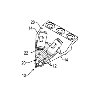
The preferred embodiment of contactless loop probe
according to the invention which is shown by way of example
in Figs. 1 to 3, for the contactless coupling-out of an RF
signal from a signal conductor or guide (not shown) for a
contactless measuring system, comprises a coupling
structure 10, two first signal conductors or guides 12
which are each connected to one end of the coupling
structure 10, and two outputs 14 which are connected to
respective ones of the first signal conductors or guides
12. The two ends of the coupling structure 10 will be
referred to in what follows as the "first port 16" (Figs.
4, 5) and "second port 18" (Figs. 4, 5). The electrical
connection between the ports 16, 18 and the first signal
conductors or guide 12 is made by respective first
transitions 20 and the electrical connection between the
first signal conductors or guides 12 and the outputs 14 is
made by respective second transitions 22. All the above-
mentioned parts are arranged on or in a housing 28 of the
loop probe.
In accordance with the invention, the coupling
structure 10 takes the form of an RF waveguide having at
least one signal conductor or guide 24 and at least one
reference conductor or guide 26.
The coupling structure 10, the first transitions 20,
the first signal conductors or guides 12, the second
transitions 22 and the outputs 14 all have impedances which
are matched to one another, thus enabling high directional
CA 02732189 2011-01-27
W02010/015315 12 PCT/EP2009/005144
attenuation to be achieved. The contactless loop probe
according to the invention is thus impedance-controlled.
Shown in Figs. 4 and 5 are two illustrative
embodiments of coupling structure in the form of a planar
line. The planar line comprises a centre conductor 24 and
an outer conductor 26, which end at the first port 16 and
second port 18 respectively.
Figs. 6 to 8 show an alternative embodiment for the
coupling structure 10. In this case the latter takes the
form of a co-axial conductor having a centre conductor 30
and an outer conductor 32. Formed in the outer conductor is
a rectangular opening 34 to serve as a coupling slot, the
inner conductor 30 thus being exposed in the region of the
opening 34. Figs. 9 to 11 show various embodiments for the
opening 34, which may be rectangular (Fig. 9) or oval (Fig.
10) in form or which may even comprise a plurality of
individual openings, as is shown in Fig. 11 which takes a
plurality of circular openings 34 as an example.
Figs. 12 to 14 show various embodiments of coupling
structure 10, in the form of a co-axial line having an
opening 34 in the outer conductor 32, which latter is
arranged close to a signal line 36 to couple out a signal
travelling along the signal line 36.
The contactless loop probe is used for applications in
a contactless measuring system, such as for contactless
vector network analysis for example. For this purpose, the
loop probe is positioned in the electromagnetic near field
of an electrical signal line 36 (Figs. 12 to 14). Together
with the signal line 36 it forms a coupler. Part of the
electromagnetic field of the signal line 36 is coupled out
by the loop probe and conveyed to the output ports 16, 18
of the loop probe. The contactless loop probe according to
the invention is impedance-controlled. Impedance-controlled
CA 02732189 2011-01-27
W02010/015315 13 PCT/EP2009/005144
loop probes have certain advantages over non-impedance-
controlled probes. Amongst other things, it is possible to
achieve high directional attenuation, and fewer sheath
waves are produced, the probes can be more satisfactorily
defined for analytical purposes and the cut-off frequency
is higher than in the case of non-impedance-controlled
measuring probes. What impedance-controlled means is that
the measuring probes are optimised for low reflection and
high directional attenuation, i.e. an impedance-controlled
io loop probe has a low insertion loss. The impedance-
controlled coupling structure 10 may be of virtually any
desired shape.
The co-axial contactless loop probe which is shown in
Figs. 6 to 14 takes the form of a screened, impedance-
controlled, co-axial near-field measuring probe. This probe
comprises the co-axial line 30, 32 which has a defined
coupling slot 34 or defined coupling holes 34. Examples of
different coupling geometries are shown in Figs. 9 to 11.
The co-axial contactless loop probe serves for use as a
coupler in the near field of the RF or microwave line 36.
Seen in combination with the centre conductor 30 of the co-
axial line, the coupling opening 34 or coupling openings 34
are sized in such a way that the co-axial contactless loop
probe (measuring probe) has high power transmission with a
low reflection factor between port 1 16 and port 2 18, i.e.
the geometry of the centre conductor 30 may be modified in
the region of the coupling opening(s) 34 in comparison with
its geometry in the rest of the co-axial line. The entire
measuring probe has inductive and capacitive coupling
properties and acts as a loop coupler.
In conventional, non-impedance-controlled loop
couplers, the coupling structure comprises one or two co-
axial conductors having continuous or connected centre
CA 02732189 2011-01-27
W02010/015315 14 PCl/EP2009/005144
conductors. To enable coupling to take place to a second
line, the outer screen (outer conductor) of the co-axial
line is completely removed. This results in a wave
discontinuity in the line and hence in reflections. In the
s case of the loop coupler shown in Figs. 6 to 8, only a
window 34 is removed from or cut out of the co-axial screen
32, and only low reflections are thus produced if a wave is
fed to the first port 16 or the second port 18. These
reflections can be minimised to a further degree by
lo changing the geometry of the centre conductor. Various
embodiments are shown in Figs. 12 to 14. As an option, the
co-axial line may be surrounded by an absorbent housing in
the case of the impedance-controlled loop probe.
In the case of the impedance-controlled loop probe
is shown in Figs. 1 to 3, the coupling structure 10 takes the
form of a planar, impedance-controlled, two-wire loop
having an impedance-controlled transition to two planar co-
planar lines which are connected in turn, by means of an
impedance-controlled transition, to two co-axial lines 12.
20 The shape of the two-wire loop 10 may be as desired.
Examples of two different shapes are shown in Figs. 4 and
5.
The coupling structure is so designed that the
coupling-out of an electromagnetic wave from a waveguide 36
25 (the input line to a DUT) is possible. The coupling
structure 10 has at least two further waveguides 12 which
are coupled to the said coupling structure 10. The
waveguides 12 connected to the coupling structure 10 are
generally equipped with a wave transition 14 to connect the
30 probe to a measuring system or to complex terminating
impedances. The probe which is shown by way of example thus
comprises at least one coupling structure 10 having at
least two waveguides 12 and transitions 14, all the
CA 02732189 2011-01-27
W02010/015315 15 PCT/EP2009/005144
components being designed together to be impedance-
controlled. Impedance-controlled means that if power is fed
into any desired waveguide of the coupling structure 10,
only very little power is reflected and high directional
attenuation is obtained if all the other wave guides are
terminated by controlled impedances.
Rather than being connected to two waveguides 12, the
coupling structure 10 may also have impedance-controlled
connections to a plurality of waveguides 12, i.e. the loop
lo probe may have more than two outputs 14.
In a preferred embodiment, the measuring probe has
only one output 14, the coupling structure 10 or rather one
of the ports 16, 18 having an impedance-controlled
termination within the housing 28 of the measuring probe.
The loop probe may also have more than one impedance-
controlled coupling structure 10. The individual coupling
structures 10 are then connected together by an impedance-
controlled waveguide or a second signal conductor or guide.
More than one loop probe may be accommodated in a
common housing 28 and for example, if the coupling
structures 10 are coupled electromagnetically to a further
waveguide 36 on a measuring substrate, a contactless
impedance-controlled twin directional coupler is produced.
The measuring probes may include a device (a sensor)
for checking distance. Various sensors are conceivable:
optical, electrical, mechanical, electromechanical etc.
ones. The distance information may be passed to the
measuring system electrically, mechanically, optically or
acoustically.
As an option, the impedance-controlled contactless
loop probe may include in addition sensors with which it is
possible to ensure exact three-dimensional positioning in
space. These sensors comprise for example a miniature
CA 02732189 2011-01-27
W02010/015315 16 PCT/EP2009/005144
camera for detecting positioning marks by pattern
recognition processes. Automated positioning of the probe
is possible by means of the probes.
To suppress sheath waves, the outer housing is
s sheathed with amongst other things ferrite and/or absorbent
materials.
The impedance-controlled contactless loop probe may be
of any desired shape and may comprise various waveguides
such for example as hollow waveguides, co-axial conductors,
io planar lines.
The coupling geometry is optimised for low reflection
(impedance-controlled) and for high directional attenuation
when a loop probe is coupled to another waveguide such for
example as hollow waveguides, co-axial guides or planar
is lines.
The geometry of the housing 28 may be of any desired
form.
When the coupling structure takes a planar form, the
individual planar lines are electrically connected by, for
20 example, (bond) wires.
The field in which the impedance-controlled loop probe
is preferably used is metrology and EMC technology, and for
the production of directional couplers.
As shown in Figs. 1 and 2, the housing 28 of the
25 measuring probe may have a mounting for fastening the
measuring probe to/into a measuring system.
The first transition 20 between the coupling structure
and the waveguides 12 may be of any desired type, in
which case it is always impedance-controlled. The
30 transition is for example soldered, brazed, welded or
adhesive-bonded.
To improve the dynamic measurement characteristics,
the coupled-out signals are amplified by means of a
CA 02732189 2011-01-27
W02010/015315 17 PCT/EP2009/005144
measurement amplifier. For this purpose, an amplifier is
implemented in the impedance-controlled loop probe, such
for example as in the individual waveguides 12 connected to
the coupling structure 10. This amplifier too is impedance-
s controlled, i.e. its impedance is matched to the input
impedance of the probe and there are thus low input
reflections and high directional attenuation. The probe is
then an active measuring probe.
In a preferred refinement of the invention, the
contactless loop probe is combined with a positioning
arrangement and the probe can thus be displaced in all
dimensions or in only one or two, etc. The positioning
arrangement may be incorporated in a probe holder or in the
housing 28 or may be connected to the loop probe or the
housing 28 by a mounting. The positioning arrangement may
be capable of being operated manually and/or may be
motorised. Hence it may be active or passive. The distance
between the probe and the measurement substrate for example
may be set or adjusted with the positioning arrangement.
The positioning arrangement may include a control line for
control purposes.