Note: Descriptions are shown in the official language in which they were submitted.
CA 02732341 2011-01-27
WO 2010/018094
PCT/EP2009/060015
1
Surface covering with static control properties
Subject of the Invention
[0001] The
present invention relates to a substrate-
free surface covering having static control properties
and a process to manufacture such surface covering.
Prior art
[0002]
Surface coverings such as multiple-layer
coverings and substrate-free coverings are well known by
those skilled in the art.
[0003]
Decorative multiple layers coverings are
heterogeneous coverings and multilayer composites,
comprising generally a backing layer, usually called
"substrate", and different layers made of distinctive and
different composition, commonly, PVC-based or polyolefin-
based layers. Generally, the substrate is a non-woven or
woven fabric, felt, rubber, compact or foamable resin-
based layer.
[0004]
Substrate-free surface coverings (also called
"homogeneous" coverings) are coverings which do not
comprise a backing layer (or substrate). Such coverings
comprise a single layer (core layer) of polymer particles
and are produced by agglomerating these particles using
heat and pressure, in a double belt press device for
instance, enabling the particles to fuse together to form
a homogeneous sheet.
[0005] An
example of a process to produce substrate-
free surface covering is described in US 4 396 566, in
which thermoplastic synthetic resin particles are applied
to a moving support, passed through a heating zone,
compacted and welded under pressure, and then cooled
simultaneously under pressure.
CA 02732341 2011-01-27
WO 2010/018094
PCT/EP2009/060015
2
[0006] Substrate-free
surface coverings present the
drawback to have poor static control properties.
Generally, they are insulators. For this reason, these
surface coverings are not suitable for an electrostatic-
free environment needed in some industries which
manufacture and/or store electronics equipments,
especially in electronic manufacturing industries.
[0007] Therefore,
surface coverings having static
dissipative electric properties have been developed. For
example, GB 2 207 435 discloses a surface covering
comprising a consolidated agglomeration of individual
chips of polymeric material, wherein at least some of the
individual chips contain an antistatic agent.
[0008] Furthermore, to
increase the cleaning and
maintenance properties of homogeneous surface coverings,
it is well known that a varnish layer may be applied on
the top surface of the coverings. However, such varnish
layer has electrical insulation properties.
Aims of the invention
[0009] The present
invention provides a substrate-
free surface covering and a process to manufacture such
covering that does not have the drawbacks of the prior
art.
[0010] It provides in
particular a substrate-free
surface covering having static control properties.
[0011] It provides in
particular a substrate-free
surface covering having dissipative or conductive
properties.
[0012] The present
invention provides also a process
to manufacture a substrate-free surface covering having
static control properties.
Summary of the invention
[0013] The present
invention describes a substrate-
free conductive surface covering comprising a core layer
of particles obtained by shredding a sheet, said
particles being unfused and embedded in a polymer matrix
CA 02732341 2011-01-27
WO 2010/018094
PCT/EP2009/060015
3
wherein said particles or said polymer matrix, or both
comprises an electrically conductive material.
[0014] A
"substrate-free" surface covering is a
surface covering which do not comprise a backing layer
(or substrate) on which the particles, component of the
surface covering, are poured onto before agglomeration.
[0015]
According to particular embodiments, the
substrate-free conductive surface covering comprises one
or a suitable combination of any of the following
characteristics:
- the core layer is covered on the top side by a
polyurethane-based varnish, said varnish comprising metal
coated spherical particles;
- a conductive primer layer is present between the
polyurethane varnish top coating and the core layer of
shredded sheet particles;
- the electrically conductive material is selected from
the group consisting of metal, metal oxide, a metal
alloy, carbon, or a mixture thereof;
- the electrically conductive material is selected from
the group consisting of silver, nickel, tungsten,
aluminium, copper, gold, stainless steel, titanium,
titanium dioxide, tin, tin oxide, antimony, antimony
oxide, carbon black, carbon graphite, carbon nanotubes,
or a mixture thereof;
- the electrically conductive material is an acicular
tin oxide composition;
- the polymer matrix represents less than 50 wt% of the
total weight of the composition of said substrate-free
conductive surface covering;
- the sheet particles and/or the polymer matrix are PVC-
based or polyolefin-based;
- the substrate-free conductive surface covering
comprises a conductive coating on the back side of said
surface covering;
- the substrate-free conductive surface covering has a
conductive resistance less than 1X10¹¹ Ohm;
CA 02732341 2011-01-27
WO 2010/018094
PCT/EP2009/060015
4
- the substrate-free conductive surface covering has a
conductive resistance less than 1X10⁹ Ohm;
[0016] The
present invention describes also a
process to manufacture a substrate-free conductive
surface covering, said process comprising the steps of:
a) providing particles obtained by shredding a
sheet,
b) providing a polymer-based powder for the polymer
matrix,
c) depositing said particles on a band-shaped moving
carrier,
d) depositing the polymer-based powder on said
particles,
e) heat treating the particles and the polymer-based
powder and compacting them in a press to form
agglomerated and unfused particles (10,11) embedded in
the polymer matrix (12,14),
wherein said particles, or said polymer matrix, or both,
comprises an electrically conductive material.
[0017]
According to particular embodiments, the
process may comprise one or a suitable combination of any
of the following characteristics:
- the process comprises a step of sanding the back side
surface of the resulting conductive surface covering to a
predefined thickness;
- the dust generated in the back side sanding step is
deposited on the band-shaped moving carrier before step
c);
- the process comprises a step of coating the back side
of the surface covering with a conductive coating;
- the process comprises a step of coating the top side of
the surface covering with a polyurethane-based
composition comprising metal coated spherical particles;
- a conductive primer is applied onto the top surface of
the conductive surface covering before applying the
polyurethane-based varnish.
CA 02732341 2011-01-27
WO 2010/018094
PCT/EP2009/060015
Brief description of the figures
[0018]
Figure 1 is a schematic representation of a
double belt press device to manufacture a substrate-free
5 surface covering according to a first embodiment of the
invention.
[0019]
Figure 2 is a schematic representation of a
double belt press device to manufacture a substrate-free
surface covering according to a second embodiment of the
invention.
[0020]
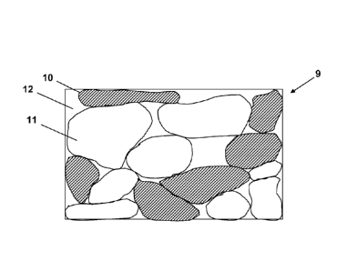
Figure 3 represents a surface covering with
static control properties.
[0021]
Figure 4 is a schematic representation of a
cross-section view of a surface covering comprising
conductive and non-conductive particles embedded in the
polymer matrix.
[0022]
Figure 5 is a schematic representation of a
cross-section view of a surface covering comprising
conductive and non-conductive particles embedded in the
conductive polymer matrix, and comprising a back side
conductive coating.
[0023]
Figure 6 is a schematic representation of a
cross-section view of a surface covering comprising
conductive and non-conductive particles embedded in a
conductive polymer matrix, and comprising a back side
conductive coating.
[0024]
Figure 7 is a schematic representation of a
cross-section view of a surface covering comprising non-
conductive particles embedded in the conductive polymer
matrix, and comprising a back side conductive coating.
[0025]
Figure 8 is a schematic representation of a
cross-section view of a surface covering comprising non-
conductive particles embedded in a conductive polymer
matrix, and comprising a back side conductive coating and
a top side conductive varnish.
[0026]
Figure 9 is a schematic representation of a
cross-section view of a surface covering comprising
conductive and non-conductive particles embedded in a
CA 02732341 2011-01-27
WO 2010/018094
PCT/EP2009/060015
6
polymer matrix, and a back side conductive coating and a
top side conductive varnish.
[0027] Figure 10 is a
schematic representation of a
cross-section view of a surface covering comprising
conductive and non-conductive particles embedded in a
polymer matrix, and comprising a back side conductive
coating, a top side conductive varnish applied over a top
coating conductive primer.
Detailed description of the invention
[0028] A decorative
surface covering, in particular
a floor covering, presents specific mechanical
properties, particularly in terms of mechanical
resistance, wear and indentation resistance, but also in
terms of comfort, softness, sound and heat insulation.
[0029] The substrate-free conductive surface
covering of the present invention combines the mechanical
properties of such substrate-free surface covering with
static control properties, and thus may be considered as
a "static control" surface covering as it can reduce, or
suppress, static charge generation and drains charges to
ground.
[0030] The conductive substrate-free surface
covering according to the present invention comprises
unfused conductive particles 10 and/or unfused non-
conductive particles 11 embedded in a polymer matrix 12
or 14, said polymer matrix may, or may not, comprise a
conductive material which improve the electrical
conductivity of said surface covering.
[0031] The non-conductive
or conductive particles
are polymer particles, preferably made of rubber-based,
PVC-based or Polyolefin-based materials. They may have a
form of a granule, fibre, shred, crumb, chip, flake, or a
pebble, of any suitable size or color.
[0032] The conductive
particles 10 further comprise
conductive material which can be, for example, a metal, a
metal oxide, a metal alloy, carbon, or a mixture thereof.
The conductive material may have high conductive
CA 02732341 2011-01-27
WO 2010/018094
PCT/EP2009/060015
7
properties; however to fulfil specific requirements, for
example aesthetical requirements, for example to get a
certain transparency, a less conductive material may be
used.
[0033] Preferably, the
conductive particles comprise
silver, nickel, tungsten, aluminium, copper, gold,
stainless steel, titanium, titanium dioxide, tin, tin
oxides, tin dioxide, antimony, antimony oxides, antimony-
pentoxide, carbon black, carbon graphite, carbon
nanotubes, or a mixture thereof.
[0034] The conductive
material represent between
1%wt and 40% wt of the weight of a conductive particle.
[0035] The conductive
particles 10 have any suitable
shape, size and thickness to form a network to conduct
electric charges from the top surface to the lower
surface of the surface covering. The conductive particles
10 have a size between around 1 and around 3 mm and an
electrical resistance between around 0.01 and around 100
Mohms.
[0036] The conductive
particles 10 represent less
than 50 wt % of the total weight of the surface covering.
[0037] Preferably, the
non-conductive particles 11
are made from a sheet of a composition comprising a
polymer, PVC-based polymer, or polyolefin-based polymer,
which is manufactured before being granulated, or
shredded, into said non-conductive particles. Preferably,
the sheet is manufactured by calendering from a
continuous polymer stream coming from an extruder device.
[0038] Preferably, the
conductive particles 10 are
made from a sheet of a composition comprising a
conductive material and a PVC based polymer or a
polyolefin based polymer. The conductive material, having
the form of a powder or a fibre, is incorporated into the
polymer particles by an extruder device followed be a
calender.
[0039] The non-
conductive 11 or conductive particles
10 may further comprise a filler, a stabilizer, a
CA 02732341 2011-01-27
WO 2010/018094 PCT/EP2009/060015
8
pigment, or a mixture thereof. A PVC-based composition
may further comprise a plasticizer.
[0040] Preferably, the filler represents between 0
and 200 Phr, the stabilizer between 0.5 and 5 Phr, the
pigment between 0 and 10 Phr, the plasticizer between 10
and 60 Phr, the unit "Phr" meaning "proportion by
weight", with respect to 100 parts of the polymer (PVC or
polyolefin).
[0041] Typical non-conductive particles (NCP) or
conductive particles (CP) compositions are given in
tables 1 and 2.
NCP-1 NCP-2 NCP-3 CP-1 CP-2
in Phr in Phr in Phr In Phr In Phr
PVC 100 100 100 100 100
Plasticizer 40 30 50 40 30
Stabilizer 3 2 4 3 3
Fillers 60 20 150 50 30
Pigment 4 1 7 0 0
Conductive 0 0 0 10 20
material
Table 1: Compositions for PVC-based non-conductive
particles (NCP) or conductive particles (CP).
NCP-A NCP-B NCP-C CP-D
in Phr in Phr in Phr in Phr
Polyolefin 100 100 100 100
Stabilizer 2 1 1 1
Fillers 50 0 150 50
Pigment 4 5 3 0
Conductive 0 0 0 20
material
Table 2: Compositions for polyolefin-based non-conductive
particles (NCP) and conductive particles (CP).
[0042] As an example, the PVC polymer is the one
from Hydro Polymers, Ineos, Georgia Gulf or Solvin.
Preferably, the polyolefin polymer is polyethylene or
CA 02732341 2011-01-27
WO 2010/018094
PCT/EP2009/060015
9
polyethylene co-octene (PE-co-0), for example AffinityTM
EG 8100 from Dow Chemical.
[0043] The filler is any suitable filler.
Preferably, it is selected among hydrates, oxides, clays,
carbonates, dolomite or talc or a mixture thereof. As an
example, the filler is dolomite (Myanite A20) from Omya
AB, chalk as Danchalk0 P from Dankalk or as Reosorb 90
from Omya AB.
[0044] The
stabilizer is any suitable stabilizer.
Preferably, it is a Ca-Zn stabilizer, for example the Ca-
Zn stabilizer from Akcros or from Barlocher GmbH.
[0045] The
pigment is any suitable pigment only
limited to aesthetic considerations. Preferably, it is
titanium oxide, C.I.Red 144, C.I.Blue 15:1, C.I. Black 7,
C.I. Green 7, C.I. Yellow 83 or C.I. Violet 23. For
example, titanium dioxide is Kemira 660 from Kemira
Pigments, Ilona 168 from Millenium Chemicals or Tronox0
R-FK-3 from IMCD Sweden AB, the Blue 15:1 is Irgatith
Blue BCA from Ciba or the PV Fast Blue from Clariant, the
C.I.Red 144 is Cromophtal0 Red BRNP from Ciba, and C.I.
Black 7 is Printex0 U from Evonik.
[0046] The
plasticizer is any suitable plasticizer.
Preferably it is DINP (Di-isononylphtalate) or DIDP (Di-
isodecylphtalate), for example from Exxon Mobile or Oxeno
GmbH.
[0047] For
conductive particles, the conductive
material is preferably carbon black, carbon nanotubes, or
electroconductive titanium dioxide in the form of a
powder or a fibre, as for example as described in
U54373013, or as known as ZelecO ECP from Milliken.
[0048] The
polymer matrix 12, wherein the non-
conductive particles 11 and the conductive particles 10
are embedded, is a PVC-based or a polyolefin-based
composition. A preferred polyolefin is polyethylene or a
co-polymer thereof.
[0049] The
polymer matrix 12 is made from a powder
comprising a particle size lower than the one of the
CA 02732341 2011-01-27
WO 2010/018094
PCT/EP2009/060015
conductive particles. Preferably, the particle size of
said powder is between 1 and 300pm.
[0050] The
polymer matrix 12 represents less than
50% wt of the total weight of the composition of the
5 surface covering 9.
[0051] The
polymer matrix composition may, or may
not, comprise at least one conductive material improving
the electrical conductivity of said surface covering.
[0052] The
conductive material is any suitable
10 material of any suitable shape, size or form, for example
it may be in the form of a powder or a fiber. It may be
the same material as the conductive material of the
conductive particles. It may represent between 1 and 40
Phr.
[0053] In the
form of a fibre, the conductive
material has a diameter between 0.01 and 1pm, preferably
around 0.3 pm, and a length between 0.05 and 10m,
preferably around 5.15 pm.
[0054] The
polymer matrix composition may further
comprise a plasticizer, a stabilizer or a mixture
thereof.
[0055] The
stabilizer may preferably represent
between 0.5 and 5 Phr. For a PVC-based composition, the
plasticizer may preferably represent between 5 and 50
Phr.
[0056]
Typical polymer matrix compositions are given
in tables 3 and 4.
Powder 1 Powder 2 Powder 3
Powder 4 Powder 5
in Phr in Phr in Phr in Phr in Phr
PVC 100 100 100 100 100
Plasticizer 35 40 40 5 50
Stabilizer 2.5 2 2 1 3
Conductive 13 20 5 40 15
material
Pigment 0 0 1 1 0
Table 3: PVC-based polymer matrix powder compositions
CA 02732341 2011-01-27
WO 2010/018094
PCT/EP2009/060015
11
Powder A Powder B Powder C
in Phr in Phr in Phr
Polyolefin 100 100 100
Stabilizer 2 2 1
Conductive 5 15 30
material
Pigment 0 1 0
Table 4: Polyolefin-based polymer matrix powder
compositions
[0057] As an
example, the PVC polymer is the one
from Hydro Polymers, Ineos, Georgia Gulf or Solvin.
Preferably, the polyolefin polymer is polyethylene or
polyethylene co-octene (PE-co-0), for example AffinityTM
EG 8100 from Dow Chemical.
[0058] The
stabilizer is any suitable stabilizer.
Preferably, it is a Ca-Zn stabilizer, for example the Ca-
Zn stabilizer from Akcros or from Barlocher GmbH.
[0059] The
pigment is any suitable pigment only
limited to aesthetic considerations. Preferably, it is
titanium dioxide, C.I.Red 144, C.I.Blue 15:1, C.I. Black
7, C.I. Green 7, C.I. Yellow 83 or C.I. Violet 23. For
example, titan oxide is Kemira 660 from Kemira Pigments,
Ilona 168 from Millenium Chemicals or Tronox0 R-FK-3
from IMCD Sweden AB, the Blue 15:1 is Irgatith Blue BCA
from Ciba or the PV Fast Blue from Clariant, the C.I.Red
144 is Cromophtal0 Red BRNP from Ciba, and C.I. Black 7
is Printex0 U from Evonik.
[0060] The
plasticizer is any suitable plasticizer.
Preferably it is DINP (Di-isononylphtalate) or DIDP (Di-
isodecylphtalate), for example from Exxon Mobile or Oxeno
GmbH.
[0061]
Preferably, the conductive material is
electroconductive titanium dioxide in the form of a
powder or a fibre, as for example as described in
U54373013, or as known as ZelecO ECP from Milliken.
[0062] In a
first embodiment, the substrate-free
surface covering comprises conductive particles 10 and
CA 02732341 2011-01-27
WO 2010/018094
PCT/EP2009/060015
12
non-conductive particles 11 embedded in a polymer matrix
12, said matrix does not comprise conductive material
improving the electrical conductivity of said surface
covering.
[0063] In a second
embodiment, the surface covering
comprises only conductive particles 10 embedded in a
polymer matrix 12 which does not comprise conductive
material improving the electrical conductivity of said
surface covering.
[0064] In a third
embodiment, the surface covering
comprises conductive particles 10 and non-conductive
particles 11 embedded in a polymer matrix 12 comprising
conductive material improving the electrical conductivity
of said surface covering.
[0065] In a fourth
embodiment, the surface covering
comprises non-conductive particles 11 embedded in a
polymer matrix 12 comprising conductive material
improving the electrical conductivity of said surface
covering.
[0066] In a fifth
embodiment, the surface covering
comprises only conductive particles 10 embedded in a
polymer matrix 12 comprising conductive material which
improving the electrical conductivity of said surface
covering.
[0067] The substrate-
free surface covering according
to the invention is produced using any suitable device.
Preferably, as shown in figures 1 and 2, it is produced
using a double belt press comprising a band-shaped moving
carrier 3 (or lower belt) made of steel or comprising a
release paper for example, a roller 1 moving the lower
belt 3, a roller 2 moving a upper belt 4, said roller 2
being heated and operating at a temperature between 160
and 200 C and a pressure of between 0.5 and 25 bars.
[0068] To manufacture
the substrate-free surface
covering according to the present invention, no bottom
layer, or substrate, is used. The conductive particles 10
and the non-conductive particles 11 are scattered onto
the band-shaped moving carrier 3, in a quantity of
CA 02732341 2016-02-25
13
between 1 and 5 Kg/m2 using either one of the device 5 or
device 7 (fig. 1) fed with a mixture of non-conductive
and conductive particles, or using the device 5 feed with
conductive particles and the device 7 (fig. 2) feed with
non-conductive particles.
[0069] Preferably, the devices 5 or 7 are fed, and
thus deposit, only the particles of the desired size. To
achieve this, during the manufacturing process of the
particles, the particles may pass through a grid, for
example a 10mm grid placed in a granulator, to select the
particles of the desired size.
[0070] The deposition of the polymer matrix powder
is performed by a device 6 which scatters the powder onto
the moving carrier 3 and the conductive particles 10
and/or non-conductive particles 11, in a quantity of
between 0.01 to 0.30 Kg/m2.
[0071] The particles and the polymer matrix powder
are then heated and compacted in a double belt press for
example, to form the substrate-free surface covering.
Thus, the conductive material of a conductive particle is
brought into contact with the conductive material of
another conductive particle to form conductive or
dissipative channels. In the same manner, the conductive
material of the polymer matrix composition is brought
into contact with another conductive material within the
polymer matrix, or is brought in contact with the
conductive material of the conductive particles, to form
conductive or dissipative channels.
[0072] The back side of the resulting substrate-free
surface covering is sanded to adjust the thickness of the
surface covering to a defined value. Preferably, around
0.2 mm of the back is removed, the final thickness of the
surface covering being between 1.9 and 2.2 mm.
[0073] To produce the substrate-free conductive
surface covering according to the present invention, no
bottom layer, or substrate, is used. However, before depositing
the particles onto the moving carrier, the non-conductive
particles 11 produced by the sanding step are deposited onto
CA 02732341 2016-02-25
14
the band shaped moving carrier 3 to form a bed of around
0.2 to 3 mm. Preferably, the non-conductive particles 11 represent
less than 10% of the total weight of the surface covering.
Preferably, the sanding dust is deposited using the
device 8.
[0074] The back side of the resulting substrate-free
surface covering, which was sanded or not, is coated with
a back side conductive coating 13 comprising conductive
material improving the electrical conductivity of the
surface covering. The conductive material is any suitable
material. It may be, for example, the same material as
the conductive material of the conductive particles 10 or
the polymer matrix 12, and may represent between 10 and
100Phr.
[0075] The back side conductive coating 13 is a
polyurethane-base coating, preferably it comprises a PU-
dispersion or a PU-solution of a two-component PU, a PU
acrylate, an epoxy acrylate, a polyester acrylate, a
polyether acrylate, a silicone acrylate, or a mixture
thereof. Preferably, the back side coating comprises a
water-based UV-curable PU acrylate dispersion with a dry
content of between 5% and 80% wt, preferably between 20
and 60% wt.
[0076] The back side conductive coating 13 is
applied by any suitable means, for example at around
20g/m2. Preferably, this back side coating 13 has a
thickness of about 6pm.
[0077] Preferably, the top side of the substrate-
free surface covering, with or without embossment, is
coated with a conductive varnish layer 15, preferably a
polyurethane-based layer, comprising conductive spherical
particles 16.
[0078] Preferably, the varnish layer 15 has a
thickness of around 10 pm and is applied by any suitable
technique, for example roller coating, reverse and
inverse spraying, curtain, screen.
[0079] The top coating 15 comprises a PU-dispersion
or a PU-solution of a two-component PU, a PU acrylate, an
CA 02732341 2011-01-27
WO 2010/018094
PCT/EP2009/060015
epoxy acrylate, a polyester acrylate, a polyether
acrylate, a silicone acrylate, or a mixture thereof
Preferably, the top coating comprises a water-based UV-
curable PU acrylate dispersion with a dry content of
5 between 5% and 80% wt, preferably between 20 and 60% wt.
[0080] The top coating
15 comprises metal coated
spherical particles 16 having a dry bulk resistivity
between 0.0001 and 0.01 ohms/cm. The spherical particles
16 are of any suitable material, however glass particles
10 are preferred. Preferably, they have a particle size
between 1 to 100m. Preferably, They represent between
0.01 and 10% wt of the total weight of the top coating.
However, their concentration in the top coating
composition and their size may be adapted to fit with the
15 thickness of the top coating desired.
[0081] The spherical
particles 16 may be coated with
any suitable metal, but preferably they are coated with
silver, aluminium, copper, nickel, gold or an alloy
thereof with another metal.
[0082] In a preferred
embodiment, before applying
the varnish layer 15, the top side of the surface
covering is coated with a top coating conductive primer
17. This primer allows to connect the spherical particles
in the top coating 15 with the conductive channels made
by the conductive material of the conductive particles 10
and/or the conductive material of the polymer matrix 12,
thus improving the conductive properties of the surface
covering.
[0083] The top coating
conductive primer 17
comprises conductive material. The conductive material is
any suitable material. It may be, for example, the same
material as the conductive material of the conductive
particles or the polymer matrix, and may represent
between 1 and 10000 Phr. Preferably, it is
electroconductive tin oxide such as described in
JP56120519, more preferably, it is an acicular type
electroconductive tin oxide composition comprising tin
oxide and antimony pentoxide.
CA 02732341 2011-01-27
WO 2010/018094
PCT/EP2009/060015
16
[0084] The
top coating conductive primer 17 is
preferably a polyurethane-base coating, preferably it
comprises a PU-dispersion or a PU-solution of a two-
component PU, a PU acrylate, an epoxy acrylate, a
polyester acrylate, a polyether acrylate, a silicone
acrylate, or a mixture thereof.
[0085]
Preferably, the top coating conductive primer
comprises a water-based UV-curable PU acrylate dispersion
with a dry content of between 1% and 40% wt, preferably
between 3 and 25% wt.
[0086]
Preferably, the thickness of the top coating
conductive primer 17 is around 2 pm and may be applied by
any suitable technique.
[0087] The
top coating conductive primer 17 may be
substantially transparent or translucent.
[0088] The
use of the top coating conductive primer
17 in combination with the top coating gives to
substrate-free surface covering not only enhanced static
control properties but also excellent cleaning and
maintenance properties.
[0089]
According to ANSI/ESD S7.1 standard, a
surface covering having a resistance to ground less then
1x10⁶ ohms is considered as a "conductive" covering, and
a surface covering having a resistance to ground less
then 1x10⁹ ohms is considered as a "dissipative"
covering. Furthermore, it generally admitted that an
"anti-static" surface covering have a resistance to
ground between 1x101 to 1x10¹² ohms, and that above 1x10¹²
ohms, the surface covering is considered as "insulator".
[0090] The
substrate-free surface covering according
to the invention are at least anti-static coverings, but
in majority, they are either dissipative or conductive
coverings as their conductive resistance are between 0.02
MQ. and 27 MQ., and a surface resistance between 0.07 MQ.
and 102 MQ..
CA 02732341 2011-01-27
WO 2010/018094
PCT/EP2009/060015
17
Examples
[0091] Example 1
A substrate-free surface covering is manufactured using
PVC-based non-conductive particles comprising 48%wt PVC
polymer from Hydro Polymers, 19% wt DINP (di-
isononylphtalate) from Exxon Mobile as plasticizer, 2%wt
of CaZn stabilizer from Akcros, 20%wt dolomite (Myanite
A20) from Omya AB and 9%wt chalk (Danchalk0 P) from
Dankalk as fillers, and as pigments 1.9 %wt of titanium
dioxide (Kemira 660) from Kemira Pigments and 0.1 %wt of
C.I. Blue 15:1 (Irgatith Blue BCA) from Ciba. The non-
conductive particles are deposited using a device 5 (feed
station), at a quantity of 3.6 Kg/m2, onto a lower steel
belt of 2.5 meters wide and running at a speed of 10
meters/min to form a bed of around 3 mm. On a subsequent
feeding station 6, the PVC-based polymer matrix powder,
comprising 66 wt% of PVC from Hydro Polymers, Ineos,
22wt% of DINP (di-isononylphtalate) from Exxon Mobile as
plasticizer and 2%wt of CaZn stabilizer from Akcros
Chemical, and 10% wt of acicular type electroconductive
titanium dioxide from Union Chemical as conductive
material, is scattered onto the non-conductive particles
in a quantity of 60 g/m2. The non-conductive particles
and the polymer matrix powder are pressed at around 10
bars between the lower steel belt and the upper steel
belt which is heated up to around 175 C on a distance of
around 7 meters. After this heating process, the sheet
produced is cooled down to about 30 C in the double-belt
press. The back side is sanded to remove around 0.2 mm so
that the thickness of the surface covering is around 2
mm. The back side is then coated with the back side
conductive coating (20g/m2) comprising 15 %wt of carbon
black.
[0092] Example 2
Example 2 is performed in the same way than example 1,
except the fact that the polymer matrix powder containing
the conductive material is scattered onto the non-
conductive particles in a quantity of 90g/m2.
CA 02732341 2011-01-27
WO 2010/018094
PCT/EP2009/060015
18
[0093] Example 3
Example 2 is performed in the same way than example 1,
except the fact that the polymer matrix powder containing
the conductive material is scattered onto the non-
conductive particles in a quantity of 120g/m2.
[0094] Example 4
Example 4 is performed in the same way than example 2
except the fact that the substrate-free covering further
comprises a top coating (20g/m2 wet) comprising spherical
particles coated with silver as conductive material.
[0095] Example 5
Example 5 is performed in the same way than example 1
except the fact that a polyurethane-base top coating
conductive primer, comprising 40%wt of a water-based
acicular tin oxide composition, comprising around 20% wt
of tin oxide and around 0.7% wt of antimony pentoxide, is
applied (12g/m2 wet) before applying the top coating
(20g/m2 wet) comprising spherical particles coated with
silver.
[0096] Example 6
Example 6 is performed in the same way than example 4
except the fact that a polyurethane-base top coating
conductive primer, comprising 40%wt of a water-based
acicular tin oxide composition comprising around 20% wt
of tin oxide and around 0.7% wt of antimony pentoxide, is
applied (12g/m2 wet) before applying the top coating
comprising spherical particles coated with silver.
[0097] Example 7
Example 7 is performed in the same way than example 1,
except the fact that the polymer matrix powder comprises
13% wt of the electroconductive titanium dioxide as
conductive material, and in that the powder is scattered
onto the conductive particles in a quantity of 30g/m2.
[0098] Example 8
Example 8 is performed in the same way than example 7,
except the fact that the polymer matrix powder containing
the conductive material is scattered onto the conductive
particles in a quantity of 60g/m2.
CA 02732341 2011-01-27
WO 2010/018094
PCT/EP2009/060015
19
[0099] Example 9
Example 9 is performed in the same way than example 7,
except the fact that the polymer matrix powder containing
the conductive material is scattered onto the conductive
particles in a quantity of 90g/m2.
[00100] Example 10
Example 10 is performed in the same way than example 7,
except the fact that the polymer matrix powder containing
the conductive material is scattered onto the conductive
particles in a quantity of 120g/m2.
[00101] Example 11
Example 11 is performed in the same way than example 9,
except the fact that the substrate-free covering further
comprises a top coating (20g/m2 wet) comprising silver
coated spherical particles as conductive material.
[00102] Example 12
Example 12 is performed in the same way than example 11,
except the fact that a water-based top coating conductive
primer comprising 40%wt of a water-based acicular tin
oxide composition, comprising around 20% wt of tin oxide
and around 0.7% wt of antimony pentoxide, is applied
(12 g/m2 wet) before applying the top coating (20g/m2 wet)
comprising silver coated spherical particles.
[00103] Example 13
A substrate-free surface covering is manufactured using
PVC-based non-conductive particles as described in
example 1, and PVC-based conductive particles comprising
35%wt PVC polymer from Hydro Polymers, 13% wt of carbon
black, 19% wt DINP (di-isononylphtalate) from Exxon
Mobile as plasticizer, 2%wt of CaZn stabilizer from
Akcros, 20%wt dolomite (Myanite A20) from Omya AB and
9%wt chalk (Danchalk P) from Dankalk0 as fillers, and as
pigments 1.9%wt of titanium dioxide (Kemira 660) from
Kemira Pigments and 0.1%wt of C.I. Blue 15:1 (Irgatith
Blue BCA) from Ciba. The non-conductive particles and the
conductive particles are deposited using a device 5 (feed
station), at a quantity of 3.6 Kg/m2, onto a lower steel
belt of 2.5 meters wide and running at a speed of 10
CA 02732341 2011-01-27
WO 2010/018094
PCT/EP2009/060015
meters/min to form a bed of around 3 mm. The conductive
particles represent around 30 % wt of the total weight of
the mixture conductive and non-conductive particles. On a
subsequent feeding station 6, the polymer matrix powder
5 comprising 66 wt% of PVC from Hydro Polymers, 22wt% of
DINP (di-isononylphtalate) from Exxon Mobile as
plasticizer, 2%wt of CaZn stabilizer from Akcros
Chemical, 10% wt of acicular type electroconductive
titanium dioxide from Union Chemical as conductive
10 material, is scattered onto the conductive and non-
conductive particles in a quantity of 120g/m2. The
conductive and non-conductive particles and the polymer
matrix powder are pressed at around 10 bars between the
lower steel belt and the upper steel belt which is heated
15 up to around 175 C on a distance of around 7 meters.
After this heating process, the sheet produced is cooled
down to about 30 C in the double-belt press. The back
side is sanded to remove 0.2 mm so that the thickness of
the surface covering is around 2 mm. The back side is
20 then coated with the back side conductive coating
(20g/m2) comprising 15 %wt of carbon black.
[00104] Example 14
Example 14 is performed in the same way than example 13,
except the fact that the powder, applied onto the non-
conductive and conductive particles, is a no conductive
powder.
[00105] Example 15
Example 15 is performed in the same way than example 13,
except the fact that a top coating (20g/m2) comprising
silver coated spherical particles as conductive material
is applied on the top surface of the surface covering.
[00106] Example 16
Example 16 is performed in the same way than example 15,
except the fact that a water-based top coating conductive
primer, comprising 40%wt of a water-based acicular tin
oxide composition, comprising around 20% wt of tin oxide
and around 0.7% wt of antimony pentoxide, is applied
(12g/m2wet) before applying the top coating.
CA 02732341 2011-01-27
WO 2010/018094
PCT/EP2009/060015
21
[00107] Example 17
Example 17 is performed in the same way than example 14,
except the fact that a top coating (20g/m2 wet)
comprising silver coated spherical particles as
conductive material is applied on the top surface of the
surface covering.
[00108] Example 18
Example 18 is performed in the same way than example 17,
except the fact that a water-based top coating conductive
primer, comprising 40%wt of a water-based acicular tin
oxide composition, comprising around 20% wt of tin oxide
and around 0.7% wt of antimony pentoxide, is
applied(12g/m2 wet) before applying the top coating.
[00109] Test results of the examples: Table 5
Example n Conductive Surface Combination
resistance, resistance, resistance, 50% RH
50% RH 50% RH
Shoe Nr 9 Shoe Nr 10
MS/ MS/
1 240 - 5000 340 -1490 88 210
2 9.7 16 10 120
3 1.4 3.4 1.2 12
4 5 12 5.5 75
5 3.3 8.3 2.1 6
6 0.8 2.1 0.6 4
7 3000 10000 375 1900
8 27 102 8 90
9 0.70 3.20 0.90 15
10 0.20 1.10 0.40 8
11 22 63 48 380
12 1 2 0.50 3.70
13 0.02 0.05 0.60 20
14 0.04 0.16 10 50
15 0.02 0.07 0.80 110
16 0.05 0.09 0.30 3
17 0.04 0.10 4 70
18 0.05 0.15 1 8
CA 02732341 2011-01-27
WO 2010/018094
PCT/EP2009/060015
22
Keys:
1: roller
2: heated roller
3: moving carrier (lower belt)
4: upper belt
5: particles scattering device
6: polymer matrix powder scattering device
7: particles scattering device
8: sanding dust scattering device
9: substrate-free surface covering
10: conductive particles
11: non-conductive particles
12: polymer matrix
13: back side conductive coating
14: conductive polymer matrix
15: top side conductive varnish
16: spherical particles of the top side varnish
17: top coating conductive primer