Note: Descriptions are shown in the official language in which they were submitted.
CA 02732522 2016-05-25
PILEUP REJECTION IN AN ENERGY-DISPERSIVE
RADIATION SPECTROMETRY SYSTEM
FIELD OF THE INVENTION
[0001] The present invention relates to energy-dispersive radiation
spectrometry systems, such as X-ray spectrometry systems or gamma-ray
spectrometry systems, and in particular to a method for improving pileup
rejection in
an energy-dispersive radiation spectrometry system.
BACKGROUND OF THE INVENTION
[0002] Energy-dispersive radiation spectrometry systems, such as, without
limitation, X-ray spectrometry systems or gamma-ray spectrometry systems, are
used
for detecting, measuring and analyzing radiation emissions, such as X-ray
emissions
or gamma-ray emissions, from, for example, a scanning electron microscope
(SEM).
A typical energy-dispersive radiation spectrometry system includes the
following four
main components: (1) a detector, (2) a pre-amplifier, (3) a pulse processor,
and (4) a
computer-based analyzer. For convenience only, and not for purposes of
limitation,
the following description will relate to X-ray spectrometry systems and
photons in the
form of X-rays (as compared to, for example, photons in the form of gamma-rays
that
are detected in a gamma-ray spectrometry system).
[0003] The detector, which usually takes the form of a semiconductor
sensor of some type, converts an incoming X-ray into a very small current
pulse,
typically on the order of tens of thousands of electrons, with a duration of
about tens
to a few hundreds of nanoseconds. The magnitude of each of the current pulses
is
proportional to the energy of the X-ray.
[0004] The pre-amplifier amplifies the current pulse output by the detector
and typically converts it into a voltage signal in the range of tenths of
millivolts up to
a few hundreds of millivolts. There are two main types of preamplifiers: "tail
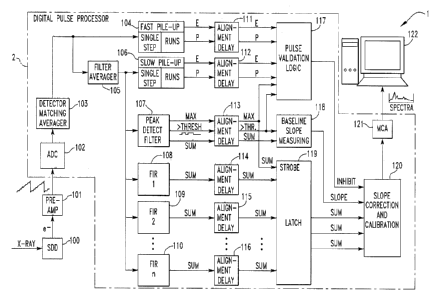
pulse"
or RC-coupled preamplifiers, and pulsed-reset preamplifiers. The subject
matter
described elsewhere herein applies to both types of preamplifiers.
[0005] In a pulsed-reset type of preamplifier, the charge generated in the
-sensor is integrated in a feedback capacitor such that the resulting voltage
increases in
1
CA 02732522 2016-05-25
steps of varying heights and intervals, until it reaches an upper limit. When
that limit
is reached, a "reset" pulse is applied which drains the accumulated charge
from the
feedback capacitor, restoring the preamplifier to near its minimum output
voltage in a
short time, typically a few microseconds. Then, charge due to the interaction
of X-
rays with the detector accumulates on the feedback capacitor again, and the
cycle
repeats. In contrast, tail-pulse preamplifiers act as high-pass filters on the
voltage step
signal output by the detector, with an exponential return to baseline whose
time
constant is long compared to the charge integration time in a feedback
capacitor of the
preamplifier.
[0006] The pulse processor receives the pre-amplifier signal and generates
a numeric representation of the X-ray's energy through an integration process.
In
older energy-dispersive radiation spectrometry systems, the pulse processor
included
two separate components, namely a "shaping amplifier" and an analog to digital
converter. Modem energy-dispersive radiation spectrometry systems, on the
other
hand, typically combine these functions, with the newest designs digitizing
the
preamplifier signal directly and carrying out all pulse detection and
filtering functions
using digital signal processing.
[0007] The computer-based analyzer accumulates the X-ray-energies output
by the pulse processor into a spectrum or plot of the number of X-rays
detected
against their energies. The spectrum is divided into a somewhat arbitrary
number of
small ranges called "channels" or "bins." In older systems, a hardware
component
called a multi-channel analyzer (MCA) did the accumulation of X-rays into
spectrum
channels and a computer read out the summed result. In modem systems, the MCA
function is handled in software, either by the computer or even within the
pulse
processor.
[0008] The job of the pulse processor is made more complex by several
factors. For example, electronic noise is superimposed on the underlying
signal
received from the preamplifier. For X-rays that are near the lowest detectable
energy
level, the preamplifier output step height may be significantly smaller than
the peak-
to-peak excursions of the electronic noise. In such as case, the X-ray can
only be
detected by filtering the signal for a relatively long period of time before
and after the
step, to average away the contribution of the noise. The amount of such noise
2
CA 02732522 2016-05-25
averaging is a fundamental operating parameter of all pulse processors. This
averaging time is variously referred to in the art as "shaping time" or
"peaking time."
[0009] Second, the steps in the preamplifier output are not instantaneous.
In the absence of noise, the signal would be a sigmoidal (S-shaped) curve.
This is due
to bandwidth limitations, device capacitance, and the time required for all
the
electrons generated by an X-ray to reach the anode of the sensor. These
electrons can
be visualized as a small cluster or cloud, which moves through the sensor
material
toward the anode under the influence of the bias voltage field within the
semiconductor sensor. With a tail-pulse preamplifier, the initial rise of the
signal is of
the same sigmoidal form, followed by an exponential decay whose time constant
may
vary with the design but is always long compared to the initial rise.
100101 In a traditional detector with simple planar electrodes on each face,
called a lithium-drifted silicon or Si(Li) detector, the bias field lines are
straight (to a
first approximation, ignoring edge effects) and run front-to-back. As a
result, the
electron cloud collection time is approximately constant, and the "rise time"
of the
preamplifier signal (the width of the sigmoidal step) is dominated by
bandwidth
limitations due to the relatively large capacitance of the device.
[0011] A new type of sensor has been developed in recent years, known as
a Silicon Drift Detector (SDD). Its salient novel characteristic is a
concentric pattern
etched into the bias electrodes which, when slightly varying voltages are
applied to
the individual rings in the pattern, permit the bias field inside the sensor
material to be
shaped such that the electrons are funneled to a very small spot anode. This
has the
effect of reducing the effective device capacitance by about four orders of
magnitude.
The electron cloud from an X-ray interaction expands with drift time to a
greater or
lesser degree depending on the path length it travels to reach the anode.
Because of
the reduced device capacitance, the cloud integration time contributes much
more to
the rise time of the preamplifier signal, which in SDDs can vary by about a
factor of
two, as compared to a few percent in the case of Si(Li) detectors (although
even the
longer end of the range of the rise time for an 'SDD may still be faster than
a
conventional planar-electrode sensor (Si(Li) detector) due to the reduced
total
capacitance).
3
CA 02732522 2016-05-25
[0012] A phenomenon known in the art as "pulse pile-up" occurs as a result
of successive X-rays arriving too close together to have their energies
measured
independently. If undetected, only one energy is measured for both X-rays,
located
somewhere between that of the higher-energy X-ray of the pair and the sum of
the
two X-ray energies, depending on the details of the pulse shaping filters of
the system
and the time interval between the X-rays. Thus, pulse processors need to be
able to
effectively detect the occurrence of pile up, which when detected, will result
in the
energy measurements associated therewith being discarded (referred to as pile
up
rejection).
[0013] Radiation, whether naturally occurring or induced by some form of
excitation, is a random process. No matter how high or low the average
emission rate,
with some non-zero probability the time interval between two emitted X-rays
can be
arbitrarily short. The probability of getting a second X-ray within any time
interval t
is:
P = (1 -e)
where e is the base of natural logarithms and r is the average X-ray arrival
rate.
[0014] The minimum time interval between two X-rays which still permits
them be identified as distinct events, which is known in the art as the "pulse-
pair
resolving time", is a strong inverse function of energy. In other words, it is
much
more difficult to detect near coincidences between small (low energy) pulses
than
large ones. Because all peak-detecting filters of a pulse processor respond
strongly to
high-energy X-rays, the most difficult case to detect is a closely following
low-energy
X-ray.
[0015] The traditional method of pile-up detection can generally be
described as one or more parallel filters with fixed but very short shaping
times
compared to the shaping time of the main energy-measurement processing path
(referred to as the "main channel"). These are variously called "fast
channels" or
"pile-up rejection channels". Each channel (main and fast) has a parameter
referred to
as dead time, which is the amount of time it takes the channel to accurately
and
unambiguously measure the energy of a single X-ray. Because the fast-channel
dead
times Df will be much shorter than the dead time D of the main channel, the
fast
4
CA 02732522 2016-05-25
channels are much more likely to produce distinct pulses for X-rays arriving
close
together in time. The filters (analog or digital) which are used in the fast
channels are
generally of the same type used for energy measurement (the main channel),
just with
much shorter pulse widths.
[0016] However, because the fast-channel shaping times are so short, they
are not very effective at averaging away electronic noise. The shaping time of
any
pulse processing channel determines the lowest energy X-ray which can be
detected
in that channel. If its detection threshold is set any lower, the processing
channel will
produce excessive false triggers due to the random noise fluctuations in the
preamplifier output signal. A state of the art X-ray spectrometry system will
typically
be able to distinguish X-rays of about 100-200 electron volts (eV) from noise
in the
main measurement channel, but the threshold energies of the fast channels must
be
much higher. The fastest pile-up rejection channel, which defines the best
pulse-pair
resolving time for high-energy X-rays, typically has a threshold between 1000-
2000
eV. Some existing pulse processors have as many as three pile-up rejection
channels
to improve pile-up rejection performance in the range below 1000 eV. In
systems
with more than one pile-up rejection channel, the intermediate channels will
have
shaping times chosen to allow sensitivity to particular emission lines such as
Oxygen
at 525 eV, or Carbon at 277 eV. With each step down in the desired energy
detection
threshold, the pulse-pair resolving time is degraded by the need for longer
shaping
time.
[0017] The pulse-pair resolving time is dominated by the lower-energy X-
ray of the pair. This is important because low-energy pile-up detection
failure affects
not only low-energy peaks, but all peaks in the spectrum. Undetected pile-up
with
low-energy X-rays can shift counts out of any peak into a broad shelf
extending from
its expected position as far as the sum of the two peak energies. A good
description
of the dependence of pile-up effects on energy may be found in P.J. Statham,
Microchim. Acta 155, 289-294 (2006).
[0018] Furthermore, the highly variable rise time for valid single X-ray
pulses in the case of SDDs, depending on how far from the charge-collection
anode
the X-ray is absorbed, poses the biggest challenge for traditional methods of
detecting
very close coincidence in time, when even the fastest conventional pile-up
channel
CA 02732522 2016-05-25
produces only a single output pulse. The classic technique, as described in,
for
example, United States Patent No. 5,684,850 to Warburton et al., is a pulse-
width
test. Digital triangle or trapezoidal filters are most popular for all-digital
pulse
processing systems, because they are relatively easy to construct and
computationally efficient. There is also what is known in the art as Finite
Impulse
Response (FIR) filters, meaning the response of the filter is guaranteed to be
zero
outside a finite range of time defined by extent of the filter's non-zero
weighting
coefficients. In contrast, traditional semi-Gaussian analog pulse shaping
introduces
exponential time constants whose response in principle continues forever,
although
in practice the output decays below the noise threshold in a reasonably
predictable
(albeit slightly energy-dependent) time.
[0019] The pulse width of FIR filters is not energy-dependent even in
principle, but it is dependent on the rise time of the preamplifier step,
which is in
turn dependent on the variable charge collection time in the SDD. Thus, in
order to
avoid false rejection of valid pulses from single X-rays, a fixed pulse-width
test
must be set long enough to accept the maximum rise time resulting from the
longest
drift path length in the SDD.
[0020] It would thus be advantageous to have a pile up detection method
that is not dependent on rise time, as such a method would improve the
performance
of systems employing SDDs wherein rise times are highly variable.
SUMMARY OF THE INVENTION
[0021] In one embodiment, a method of detecting a pileup from an output
signal of a preamplifier of an energy-dispersive radiation spectrometry
system, such
as an X-ray spectrometry system or a gamma-ray spectrometry system, wherein a
filter of the energy-dispersive radiation spectrometry system generates a
first pulse
in response to the output signal, and wherein the energy-dispersive radiation
spectrometry system has one or more fast channels, wherein each of the fast
channels has an associated energy of full efficiency that depends on a
threshold
energy associated with the fast channel wherein substantially all photons
received
by the energy-dispersive radiation spectrometry system having at least the
associated energy of full efficiency are detected by the fast channel. The
method
6
CA 02732522 2016-05-25
includes measuring an above threshold time duration which is a time during
which
the first pulse is above a minimum detectable threshold energy of the filter,
determining that at least one of the one or more fast channels has not made
any
detections while the first pulse is above the minimum detectable threshold
energy of
the filter, in response to the determining, declaring a pileup if the above
threshold
time duration exceeds a longest expected pulse duration, wherein the longest
expected pulse duration is a duration of a second pulse that would be output
by the
filter in response to a single photon being received by the energy-dispersive
radiation spectrometry system, wherein said single photon has an energy equal
to
the associated energy of full efficiency of the particular one of the one or
more fast
channels which have not made any detections that has the lowest threshold
energy.
In one particular embodiment, the one or more fast channels comprise a
plurality of
fast channels.
[0022] In another embodiment, a pulse processor is provided that is adapted
to perform the method just described. In still another embodiment, an energy-
dispersive radiation spectrometry system, such as an X-ray spectrometry system
or
a gamma-ray spectrometry system, is provided that includes a detector for
converting an incoming photon into an output comprising a current pulse, a
preamplifier for converting the output of the detector into a preamplifier
output
signal comprising a voltage signal, and a pulse processor having a filter that
generates a first pulse in response to the preamplifier output signal, and one
or more
fast channels, wherein each of the fast channels has an associated energy of
full
efficiency that depends on a threshold energy associated with the fast channel
wherein substantially all photons received by the energy-dispersive radiation
spectrometry system having at least the associated energy of full efficiency
are
detected by the fast channel. The pulse processor is adapted to measure an
above
threshold time duration which is a time during which the first pulse is above
a
minimum detectable threshold energy of the filter, determine that at least one
of the
one or more fast channels has not made any detections while the first pulse is
above
the minimum detectable threshold energy of the filter, and in response to
determining that the one or more fast channels have not made any detections,
7
CA 02732522 2016-05-25
declare a pileup if the above threshold time duration exceeds a longest
expected
pulse duration, the longest expected pulse duration being a duration of a
second
pulse that would be output by the filter in response to a single photon being
received
by the energy-dispersive radiation spectrometry system, wherein said single
photon
has an energy equal to the associated energy of full efficiency of the
particular one
of the one or more fast channels which have not made any detections that has
the
lowest threshold energy.
[0023] Therefore, it should now be apparent that the invention substantially
achieves all the above aspects and advantages. Additional aspects and
advantages
of the invention will be set forth in the description that follows, and in
part will be
obvious from the description, or may be learned by practice of the invention.
Moreover, the aspects and advantages of the invention may be realized and
obtained
by means of the instrumentalities and combinations particularly pointed out in
the
appended claims.
BRIEF DESCRIPTION OF THE DRAWINGS
[0024] The accompanying drawings illustrate presently preferred
embodiments of the invention, and together with the general description given
above and the detailed description given below, serve to explain the
principles of
the invention. As shown throughout the drawings, like reference numerals
designate like or corresponding parts.
[0025] Figure 1 is an overall block diagram of an X-ray spectroscopy
system according to one particular, non-limiting embodiment in which the
present
invention may be implemented;
[0026] Figure 2 is a block diagram of a generic trapezoidal FIR digital
filter;
[0027] Figures 3A-3D includes source code which may be used to
implement the invention according to one particular non-limiting embodiment;
[0028] Figures 4A and 4B are each a state diagram extracted from the
program logic of Figures 3A-3D which may be used to design an FPGA
embodiment of the invention;
8
CA 02732522 2016-05-25
[0029j Figure SA shows idealized trapezoidal responses from the peak
detect filter shown in Figure 1 to two low-energy X-rays of differing
energies, with a
third line showing the detection threshold energy;
100301 Figure 5B shows an idealized representation of the output of the
' peak detect filter shown in Figure 1 from two X-rays at 400 eV energy;
[00311 Figure 6A, 6B and 6C show three possible patterns of rise and local
extrema that may be processed to detect edges using one embodiment of the
present
invention;
[00321 Figures 7A and 73 show two plots of actual waveforms from an
SDD; and
9
CA 02732522 2016-05-25
[0033] Figure 8 is a schematic diagram which summarizes the expected
pile-up performance of the system of Figure 1 with typical pulse-pair
resolving times
and energy detection thresholds for a particular SDD.
DESCRIPTION OF THE PREFERRED EMBODIMENTS
[0034] As noted in the Background of the Invention, the subject matter
described herein applies to both tail pulse and pulsed reset preamplifiers.
However,
for ease of illustration and description, invention will be described in
connection with
embodiments that employ a pulsed reset type preamplifier. As discussed in the
Background of the Invention, the rising portion of the detector voltage step
signal is
passed through a tail pulse type preamplifier relatively unchanged. As a
result, it will
be appreciated from the description for the pulsed-reset embodiment that the
invention described herein may readily be applied to a tail pulse preamplifier
embodiment. In addition, the subject matter described herein applies to energy-
dispersive radiation spectrometry systems generally. However, for ease of
illustration
and description, the invention will be described in connection with
embodiments that
employ an X-ray spectrometry system. This is not to be considered to be
limiting,
and it is to be understood that the invention may be applied in connection
with other
types of energy-dispersive radiation spectrometry systems, such as, without
limitation,
gamma-ray spectrometry systems.
[0035] The improvements described herein do not depend on rise time, but
rather, in one embodiment, only on the expected sigmoidal pattern of charge
collection in the detector, and in another embodiment, on having a
monotonically
(within a noise-dependent limit) rising signal followed by a brief period
where
random noise determines the direction (sign of the local first derivative,
rising or
falling) of the signal.. Thus, improvements described herein can respond
faster to X-
ray steps with short rise times, and appropriately more slowly to pulses with
longer
rise times without falsely rejecting the latter. In one embodiment, an
assumption
which is made is that the voltage signal from a valid single X-ray should have
a
monotonically increasing first derivative (within the limits of noise) up to
some
maximum, followed by a monotonic decrease. As described in greater detail
herein,
the disclosed method according to one embodiment digitizes the preamplifier
output
CA 02732522 2016-05-25
directly, and the sequential differences between digitizing ADC samples give
the best
available estimate of the instantaneous value of the first derivative. In
another
embodiment, an assumption which is made is that the voltage signal from a
valid
single X-ray should rise above the local peak-to-peak noise band and then
eventually
stop rising, and that the noise band should shift significantly before and
after the rise,
as measured by the local maximum preceding the rise and the local minimum
following it. The system in this embodiment digitizes the preamplifier output
directly
and local extrema are measured in the digitized signal.
[0036] The conversion speed of the digitizing ADC should be properly
matched to the expected range of rise times. It should be fast enough so that
at the
shortest expected rise time, the waveform will be sampled several times during
the
rise. The minimum number of samples within a rise time for the invention to be
fully
effective is preferably 4 or 5. In a preferred embodiment, the sampling rate
of the
ADC is 100 MHz for a shortest expected rise time of approximately 50 nS, so
that 5
samples occur within the minimum rise time and roughly 10 samples in the
longest
rise time.
[0037] If the sampling rate is too high, such that say 40 or 50 samples fall
within the rise time, the waveform will not move enough in a single sampling
interval
for a rising step to be easily distinguishable from a random noise
fluctuation. As
described elsewhere herein, this situation is easily handled by dividing down
the
sampling rate, summing some number of ADC samples for each value presented to
the circuitry embodying the invention, to achieve the optimum 4 to 8 samples
in the
fastest rise.
[0038] A main object of an embodiment of the present invention is to
reduce the average pulse-pair resolving time for voltage steps generated in
the output
signal of a semiconductor radiation sensor, by exploiting the smooth sigmoidal
nature
of the underlying signal, and using an adaptive step-detection method which
automatically adjusts itself to variations in the rise time and noise
characteristics of
the sensor/preamplifier combination. The result is a lower level of undetected
pulse
pile-up in the energy spectrum and thus a reduction in the relative size of
the
erroneous artifacts known in the art as "sum peaks" which occur at twice the
energy
of, or the summed energies of any two, large emission peaks in the spectrum.
11
CA 02732522 2016-05-25
[0039] The method described herein is digitally based, and requires the
preamplifier signal to be digitized by an analog-to-digital converter (ADC).
The
optimum conversion rate is dependent on the fastest rise time expected from
the
preamplifier, as described above.
[0040] The description which follows assumes a positive-going
preamplifier output when X-rays are detected, but it will be appreciated by
those of
skill in the art that the polarity of the signals could be reversed throughout
the signal
chain and the method would be equally effective. It also assumes a Silicon-
based
sensor and radiation in the low X-ray energy range, but again it will be
appreciated by
those of skill in the art that the method described applies to sensors made of
other
semiconductors such as Germanium, and to photons of higher-energy X-rays or
Gamma rays.
[0041] Figure 1 is an overall block diagram of an X-ray spectroscopy
system 1 according to one particular embodiment in which the present invention
may
be implemented. As seen in Figure 1, the X-ray spectroscopy system 1 includes
as a
main component thereof a digital pulse processor (DPP) 2, shown by a dotted
line
boundary, in which the present invention is implemented as described herein.
In
addition, the X-ray spectroscopy system 1 further includes a silicon drift
detector
(SDD)100 and a pulsed reset-type preamplifier 101.
[0042] In operation, an X-ray strikes the SDD 100 and is converted into
electron-hole pairs, the number of electrons being proportional to the energy
of the X-
ray. The small charge consisting of the total of these electrons is
accumulated on a
capacitor in the preamplifier 101 and is converted into an output voltage
signal of the
form shown, in which small sigmoidal steps occur with varying amplitudes and
intervals superimposed on noise. The voltage signal has an overall positive
slope due
to leakage current in the SDD 100, with periodic resets which drain the charge
from
the feedback capacitor and force the output quickly to its lower limit,
resulting in the
sawtooth-like waveform shown in Figure 1. This general approach has been known
in
the art for many years.
[0043] The output of the preamplifier 101 is digitized by a high-speed
Analog-to-Digital Converter (ADC) 102 provided as part of the DPP 2. In a
preferred
embodiment, the ADC 102 is a 100 Mhz, 16-bit part made by Analog Devices such
as
12
CA 02732522 2016-05-25
the AD9446 series. The present invention was developed using a development
board
supplied by Analog Devices for this device (Model AD9446-10OLVDS/PCB),
modified to accept a DC-coupled input signal and connected to an interface
board
with an on-board memory and a standard USB interface to a PC (Model HSC-ADC-
EVALB-DC), to capture thousands of brief (2.62 millisecond) segments of
preamplifier waveforms from an SDD mounted on a scanning electron microscope
(SEM), adding up to several seconds of real time data stored in disk files.
The
subsequent digital functions described below were first embodied in post-
processing
software written in a scripting language called Python. Source code for that
software
was included in United States Provisional Application No. 60/963,320, entitled
"IMPROVED EDS PILEUP REJECTION FOR LOW ENERGIES AT HIGH
COUNT RATES", filed on August 3, 2007. Selected functions from are reproduced
herein. The Python program then served as the specification for a real-time
embodiment using a combination of field programmable gate array (FPGA) logic
and
software written for a Texas Instruments 320C-6414 digital signal processing
(DSP)
chip. The preferred embodiment, which is shown in Figure 1, places logic
blocks 103
through 119, named and described in greater detail below, in FPGA logic, and
logic
blocks 120 and 121, also named and described in greater detail below, in DSP
chip
software.
[0044] The output of the ADC 102 consists of digital samples from the
preamplifier voltage waveform and a clock which defines the timing for all
subsequent blocks in Figure 1. In order to simplify Figure 1, the clock is not
shown
separately, but all function blocks should be understood to be synchronized by
the
clock of the ADC 102 or some sub-multiple of it as described below.
[0045] The output of the ADC 102 and its clock go through a detector
matching averager 103, which optionally sums a number of ADC samples and
divides
the original ADC clock by the same number. The purpose of the detector
matching
averager 103 is to optimize the effective sampling interval with respect to
the rise
time of the SDD 100 connected to the DPP 2. Retaining all bits in the sum is
preferred in order to avoid quantization errors in the final X-ray spectrum at
very
short filtering times, so the data paths get wider as processing continues
through the
DPP 2.
13
CA 02732522 2016-05-25
[0046] If the average rise time expected from the SDD 100 is less than
about 150 nS, the detector matching averager 103 is disabled and the full 100
Mhz
rate is used in order to obtain the best possible timing precision. However,
if a much
slower detector such as the so-called lithium-drifted silicon or Si(Li)
detector with
planar electrodes is connected to the DPP 2, and the average rise time is
several
hundreds of nS, it is desirable to reduce the effective sampling rate to that
which
produces fewer than about 16 samples in the average rise.
[0047] The (possibly summed) data and clock from the detector matching
averager 103 are passed through two parallel paths. One path leads to fast
pile-up
logic 104 which has two sub-sections. The first sub-section is referred to as
single-
step logic, which is the subject of one embodiment and is described in greater
detail
herein. The other sub-section is referred to as runs logic, which is the
subject of
another embodiment comprising a digital method based on the length and pattern
of
monotonic runs of successive data samples, and is also described in greater
detail
herein. "Monotonic" as used here does not mean strictly monotonic in the
mathematical sense. The comparator employed in the method has been offset
slightly
negative to make detection of positive runs tolerant of a negative sample-to-
sample
difference if that difference is small compared to the peak-to-peak noise
fluctuations.
Where the single-step logic is capable of detecting pile-ups within a single
continuous
rise for moderately high energy X-rays, runs logic is designed to detect the
end of a
continuous rise due to a low-energy X-ray as quickly as possible within
constraints of
noise.
[0048] The second path leads to a filter averager 105. The filter averager
105 sums a small number of successive ADC samples, preferably 4, to reduce the
noise (random fluctuations from sample to sample) and also reduce the speed
required
in subsequent digital processing steps. The summed-by-4 data and the divided-
by-4
clock are passed to slow pile-up logic 106. The slow pile-up logic 106 is
functionally
identical to the fast pile-up logic 104, but with less noisy and slower data.
When
operating on the slower sample rate from the filter averager 105, the present
invention
will not have as good a resolving time, but will reach a lower energy
detection
threshold before false triggering on noise becomes excessive.
14
CA 02732522 2016-05-25
[0049] The output from the filter averager 105 is also passed in parallel to a
peak detect filter 107 (the main channel), and a plurality of trapezoidal FIR
digital
filters 108, 109, 110 (fast channels). All of these filters are of the
conventional
trapezoidal type, as has been commonly used in the art for at least 15 years.
A block
diagram of a generic trapezoidal FIR digital filter is shown in Figure 2. As
seen in
Figure 2, the ADC samples pass through three variable-length FIF0s, referred
to as
the rise FIFO 201, the gap FIFO 202 and the fall FIFO 203. The rise FIFO 201
is the
initial integration time of the FIR filter. When convolved with a step edge,
it gives a
linear rise in the final FIR sum as the edge passes through the FIFO (ignoring
noise
fluctuations). The gap FIFO 202 is a period of zero weighting which provides a
"flat
top" to what would otherwise be a triangle-shaped response to a step edge. A
flat top
is desirable because, if the rise time of the detector is variable, a pure
triangle pulse
shape (no gap) would have different maximum outputs for noise-free step edges
of the
same height but different rise times. If the gap is long enough to cover the
longest
expected rise time, the maximum output sum will be the same (ignoring noise
and any
background slope in the input signal). The fall FIFO 203 integrates samples
over the
same period as the rise FIFO 201 but with the opposite polarity, so that any
sample
which is added to the overall sum N times in rise FIFO 201 is eventually
subtracted
from it N times in the fall FIFO 203, where N is the length of the two FIF0s.
[0050] Triangle (or trapezoidal) filter shapes are popular because of the
simple circuitry required to compute them. Only four computations are required
per
FIFO clock cycle for an FIR filter of arbitrary total length. The samples
entering and
leaving the rise FIFO 201 are added and subtracted, respectively, to the
running sum.
The samples entering and leaving the fall FIFO 203 are subtracted and added,
respectively, to the running sum. The first difference is computed in
arithmetic logic
unit (ALU) 204, and the second in ALU 205. The outputs of those two ALUs are
added to the previous overall FIR output in accumulator 206.
[0051] The maximum of the FIR output sum will occur while the sigmoidal
rise of the input signal is entirely contained within the gap FIFO 202, and is
proportional to the energy of the X-ray causing the rise.
[0052] The peak detect filter 107 is not concerned with measuring the X-
ray's energy, but with detecting all X-rays, even those of very low energy,
and
CA 02732522 2016-05-25
locating them as accurately as possible in time. The width of its rise and
fall FIFOs is
made as short as possible while still reliably detecting the lowest-energy X-
ray
emission line in the spectrum being collected. For X-ray analyzers mounted on
electron microscopes, that is often the carbon emission line at 277 electron
volts (eV).
Hence the peak detect filter 107 is often referred to as the "carbon filter"
in United
States Provisional Application No. 60/963,320, entitled "IMPROVED EDS PILEUP
REJECTION FOR LOW ENERGIES AT HIGH COUNT RATES", filed on August
3, 2007 identified above. The minimum target emission line may be lower in
energy
(boron or beryllium), or higher in the case of detectors for X-ray
fluorescence (XRF)
excitation, which is very inefficient at low energies. XRF detectors are
usually
equipped with beryllium windows in front of the sensor, which block
essentially all
X-rays below about 700 eV. In that case, the peak detecting filter 107 can be
made
narrower without fear of missing significant numbers of X-rays, which improves
its
performance for pile-up detection.
10053] The peak detecting filter 107 generates the usual FIR sum and two
other signals: a pulse at the time of maximum response, and a logic signal
indicating
when its response exceeds a threshold energy. The detailed use of those
signals will
be described later.
[0054] The FIR filters 108, 109, 110, which are for measuring X-ray energy
levels, the peak detect filter 107, the slow pile-up logic 106 and the fast
pile-up logic
105 are all connected to appropriately sized programmable-length alignment
delay
FIFOs 111, 112, 113, 114, 115, 116 such that for a noise-free single X-ray
pulse of
sufficient energy to trigger all edge (event) detectors, the edge (event)
locations
(times) from the fast and slow pile-up logic 104, 106, the maximum of the peak
detect
filter 107, and the output data corresponding to the center of the gap for all
energy-
measuring FIR filters 108, 109, 110 will arrive at pulse validation logic 117,
baseline
slope measuring logic 118 and filter latch logic 119 at the same time (within
the time
quantization limit imposed by the clock division of the filter averager 105).
[0055] The filter latch logic 119 grabs the outputs of all FIR filters which
correspond to the aligned maximum-output time of the peak detect filter 107.
It is the
functional equivalent of the sample-and-hold circuit of classical analog pulse
processing. Its outputs are delayed by an additional period corresponding to
half the
16
CA 02732522 2016-05-25
FIR pulse width (fall time plus half the gap time) of the longest FIR filter
in the
energy-measurement filter stack, to allow time for detection of pile-ups
following the
edge which triggered the latch.
[00561 The filter latch logic 119 also contains timers to measure the time
from the current strobe signal to the preceding and following strobe signals
(maximum-output pulses from peak detect filter 107), in order to allow
selection of
the longest filter in the FIR stack (if any) which can be used without pile-up
according
to the methods disclosed in United States Patent No. 3,872,287 to Koem.an and
United
States Patent No. 5,393,982 to Mott. The outputs of all filters shorter than
this
maximum may also be combined with differing weights to achieve a better
estimate of
the X-ray's energy, again according to the method taught in United States
Patent No.
3,872,287 to Koeman.
100571 The baseline slope measuring logic 118 measures the positive slope
due to leakage current of the voltage signal of the preamplifier 101 in the
absence of
a sigmoidal step due to an X-ray's arrival. It is well-known in the art that
trapezoidal
:FIR filters have a constant response to a linear slope which depends on the
width of
the filter's integration time and gap. This slope response must be subtracted
from the
filter's output to obtain an accurate measure of the X-ray's energy. The
details of a
preferred method for estimating the slope near the sigmoidal step are
described in
United States Provisional Application No. 60/963,312, entitled "DIGITAL PULSE
PROCESSOR SLOPE CORRECTION", filed August 3, 2007.
100581 The pulse validation logic 117 combines the signals from the fast pile-
up logic 104, the slow pile-up 106 and the peak detect filter 107 to determine
if a pile-
up has occurred within a single output pulse from peak detect filter 107. If
such a pile-
up has occurred, which will not be detected by the filter latch logic 119
because only
one maximum output pulse will be generated by the peak detect filter 107, an
inhibit
pulse is generated and appropriately delayed to arrive at the same time the
output of
filter latch logic 119 reaches slope correction and calibration logic 120.
100591 The following tests are performed in the pulse validation logic 117.
If a direct pile-up detected pulse is received from either the fast pile-up
logic 105 or
the slow pile-up logic 106 while the "above threshold" logic signal from the
peak
17
CA 02732522 2016-05-25
detect filter 107 is active, a pile-up is declared and the inhibit signal is
generated. If
two or more edge-detected pulses are received from either the fast pile-up
logic 105 or
the slow pile-up logic 106 while the "above threshold" logic signal is active,
a pile-up
is also declared and the inhibit signal is generated.
[0060] Edge-detected signals and pile-up detected signals generated from
the fast pile-up logic 105 or the slow pile-up logic 106 when the "above
threshold"
signal is not active are ignored as false triggers. This prevents counting
false triggers
due to brief noise spikes which are averaged away to less than the energy
threshold in
the peak detecting filter 107, and allows the two pile-up logic blocks to have
lower
detection thresholds than might otherwise be necessary.
[0061] The pulse width and pulse symmetry of the output from the peak
detect filter 107 are also tested as disclosed in United States Patent No.
5,349,193 to
Mott to detect pile-up if one or both of the X-rays is too low in energy to
trigger the
fast pile-up logic 105 or the slow pile-up logic 106.
[0062] An additional symmetry-like test is performed which checks
whether edges detected in the fast pile-up logic 104 and the slow pile-up
logic 106 are
centered in the time above threshold of the peak detect filter 107. In the
software-
based implementation described elsewhere herein, this is done by taking an
absolute
difference in time of the edge positions reported by the fast pile-up logic
104 and the
slow pile-up logic 106 and the maximum response of the peak detect filter 107,
which
for a single X-ray is expected to be centered in the time above threshold.
However, it
is more convenient in the FPGA logic implementation shown in Figure 1 to use
timers
as shown in Figure 5b instead of an absolute difference of time stamps. These
timers
will be referred to as Event Lag timers. One Event Lag timer is started at the
beginning of the "above threshold" signal. When an edge signal is received
from
either the fast pile-up logic 104 or the slow pile-up logic 106, the timer is
checked
against a limit value computed from the known rise and gap times of the peak
detect
filter 107, plus half the longest expected rise time of the detector for a
single event,
plus a small allowance for variations due to noise and time quantization
errors. If
the timer exceeds this limit, a pile-up with a low-energy X-ray is assumed to
have
occurred.
18
CA 02732522 2016-05-25
[0063] A second Event Lag timer is started when any edge is received from
the fast pile-up logic 104 or the slow pile-up logic 106, and checked against
the same
limit when the "above threshold" signal goes low. The two timers are labeled
"Event
Lag 1" and "Event Lag 2" in Figure 5b. It will be clear to those of ordinary
skill in
the art that this pair of timers constrain the edge signals to a range in the
center of the
time above threshold for the peak detect filter 107. This is functionally
equivalent to
the software time-stamp method on the assumption that the maximum response of
the
peak detect filter 107 would normally be near the center of the time above
threshold.
[0064] Edge detection by any filtering mechanism does not have a sharp
cutoff in which all X-rays above a certain value are detected while all X-rays
below it
are not. Instead, due to random noise fluctuations near the edge, detection
efficiency
rolls off smoothly from 100% above some energy to zero below some lower
energy,
as described in P.J. Statham, Microchim. Acta 155, 289-294 (2006). Figure 2
from
that publication illustrates the shapes of the detection efficiency curves,
although that
figure refers to Si(Li) detectors and the constants and energy ranges will be
quite
different for SDDs. Assume pile-up of two X-rays at the energy where the slow
pile-
up logic 106 will detect them with 50% probability. Half the time only one of
the X-
rays will be detected.
[0065] Figure 5a shows idealized trapezoidal responses from the peak
detect filter 107 to two low-energy X-rays of differing energies, with a third
line
showing the detection threshold energy. The specified energies in a real
application
may differ depending on the filter width and the specific SDD/preamplifier
being
used, but the values given are reasonable for a current-generation SDD.
[0066] The upper dashed line, 480 eV, represents the energy above which
the slow pile-up logic 106 is nearly 100% efficient. The middle dashed line,
280 eV,
is near the Carbon X-ray energy. The lower dashed line, 160 eV, might be a
typical
setting for the detection threshold and is low enough to detect the element
Boron (183
eV).
[0067] The center time labeled "G+R+N" is the allowance for the gap time
G of the peak detect filter 107, the longest rise time R expected from the
detector, and
a safety factor N for noise and time quantization errors. This generates a
flat region in
19
CA 02732522 2016-05-25
the filter output. The rising and falling segments of the output are the
leading and
trailing integration times of the peak detect filter 107.
[0068] "High-energy" in the case might mean up to 20 to 30 thousand eV
(keV), more than 100 times greater than the detection threshold. The pulse
widths B
and C shown for 480 eV and 280 eV X-rays respectively will be shorter as shown
because the detection threshold becomes an increasingly significant threshold
of the
X-ray energy below 1 keV.
[0069] Figure 5B shows an idealized representation of the output of the
peak detect filter 107 from two X-rays at 400 eV energy. 400 eV is too low to
trigger
the slow pile-up logic 106 reliably, and a detection efficiency of 50% is
assumed at
this energy. The trapezoid outlined with crosses shows the response to a
single
centered X-ray of 400 eV. The dotted and dot-dashed trapezoids show two such X-
rays shifted left and right to times X1 and X2 respectively. The total
response is the
upper solid line, which is always the sum of the dotted and dot-dashed lines.
The
circled numbers show times where the slope of the output response changes.
Because the piled-up X-rays are assumed to be equal in energy, the output
shape is
symmetrical with its maximum falling somewhere in the narrow flat region
between
circles 3 and 4. Due to small random noise fluctuations, the actual maximum
can be
anywhere in this region, so a symmetry check as described in United States
Patent No.
5,349,193 may not detect the pile-up.
[0070] The pulse in the peak detect filter 107 may pass an overall pulse
width check as well. As shown in Figure 5A, the pulse width for a single low
energy
X-ray will be reduced compared to maximum width at high energies, and if low
energy piled-up events are separated by less than this reduction, the pulse-
width test
will be ineffective as shown in Figure 5B (range p-p is less than A). However,
as
shown in Figure 5B, one of the timers described above will have the entire
pulse
separation time added to the average pulse rise time above threshold for a
given X-
ray. Thus, testing these timers increases the probability of detecting pile-up
if only
one of the X-rays triggers at least one of the pile-up logic blocks.
[0071] A fixed EventLag limit cannot be less than the integration time of
the peak detect filter 107 plus the "G+R+N" time described above, or single
high-
energy X-rays may be falsely rejected as pile-up. The lower the limit, the
lower the
CA 02732522 2016-05-25
time separation which is detectable, so it is advantageous to choose an SDD
with the
fastest possible rise time R and the lowest possible noise N.
100721 A further improvement in pile-up detection can be made if the limits
against which the timers are tested is not constant, but varies with energy,
since as
discussed above and illustrated in Figure 5A the pulse width of the peak
detect filter
107 is lower for low energies. This lower pulse width is predictable from the
known
detection threshold energy and FIR integration time of the peak detect filter
107, if the
X-ray energy is known. Unfortunately, since a pile-up within the pulse time of
the
peak detect filter 107 is presumed, its maximum output may be proportional to
any
value up to the sum of the energies of the piled-up X-rays.
100731 However, an upper limit on the energy of all X-rays in the pile-up
sequence can be set by realizing that if the fast pile-up logic 105 is not
triggered, none
of the X-rays may be above the energy where its detection efficiency nears
100%.
Similarly if the slow pile-up logic 106 is not triggered, none of the X-rays
can exceed
the energy where its detection efficiency nears 100%.
[0074] In practice, this means setting two different limits for the Event Lag
timers and three for the total pulse width: the longest, equal to the fixed
limit
discussed above, for events triggering at least one fast pile-up 105 edge
detection; a
middle threshold for events triggering no fast pile-up 105 edge detection, but
at least
one slow pile-up logic 106 edge detection; and the shortest for pulse-width
testing
only when no edges are detected by the pile-up logic blocks. The reductions in
the
limits from the high-energy case are computed from the ratio of the detection
threshold energy of the peak detect filter 107 and the 100% detection-
efficiency
energy of the appropriate pile-up logic block. The expected time above
threshold for
the rising and falling portions of the FIR response of the peak detect filter
107 for a
single X-ray is shortened by the same proportion. In Figure 5A, the threshold
of 160
eV is 1/3 of the 480 eV energy limit above which the slow pile-up logic 106 is
expected to detect nearly all X-rays, so the time above threshold for the
rising/falling
portions of the output is reduced by 1/3. This comparatively large change in
expected
pulse width with energy near the lowest detectable energies enables detection
of
closer pile-ups than was possible in the prior art.
21
CA 02732522 2016-05-25
[0075] In the absence of an edge from the slow pile-up logic 106, the pulse
width above threshold should not be greater than interval B given in Figure
5A, where
the expected width of a pulse from a Carbon X-ray is interval C. Therefore,
two
Carbon X-rays separated by more than (B-C) will be detectable as pile-up. In
the
prior art, pile-up would not be detected unless the Carbon X-rays were
separated by at
least (A-C). The same reasoning applies if one X-ray triggers the slow pile-up
logic
106 but not the fast pile-up logic 105, although pulse width 13' will be
somewhat
wider because the full-efficiency energy limit of the fast pile-up 105 is
higher. Also,
the EventLag timer limit can be set to the interval from the right edge of the
center
G+R+N band to the left edge of interval B appropriate for the fast pile-up
logic 105
full-efficiency energy limit. Pile-up detection for C X-rays with 0 X-rays
will thus be
improved compared to the prior art.
[0076] Returning to Figure 1, the slope correction and calibration logic 120
receives a current slope estimate from the baseline slope measuring logic 118,
the
outputs of all energy-measuring FIR filters 108, 109, 110, and possibly an
inhibit
signal from the pulse validation logic 117, all appropriately time aligned. In
a
preferred embodiment, these functions are implemented in software in a digital
signal-
processing chip such as the Texas Instruments TMS320C6414, since these events
occur at the pulse rate of the peak detect filter 107, which is much lower
than the
ADC sampling rate.
[0077] In the absence of an inhibit signal, this logic subtracts the error due
to the baseline slope in the signal from the ADC 102 in a manner well-known in
the
art, and weights the raw outputs of one or more of the FIR filters 108, 109,
110 to
generate a calibrated energy estimate for the X-ray which produced the step
edge.
[0078] These measured energies are stored in the memory of a multi-
channel analyzer (MCA) 121, again in a manner well-known in the art. The
spectrum
accumulated in the MCA 121 is passed to a host PC 122 for analysis.
[0079] Described in detail herein are parts of the fast pile-up logic 105 and
the slow pile-up logic 106 labeled "Single Step" and "Runs" in Figure 1.
"Single
Step" is so called because it operates on the successive differences between
samples
from the ADC 102, possibly averaged as described above in the detector
matching
averager 103 and the filter averager 104. "Runs" is so called because it
tracks
22
CA 02732522 2016-05-25
positive-going and negative-going runs of samples from the ADC 102, possibly
averaged as described above in the detector matching averager 103 and the
filter
averager 104. Figures 3A-3D provide a listing of the program source code for
the
function which embodies both the "Single Step" and "Runs" portions of the fast
pile-
up logic 105 and the slow pile-up logic 106 according to one embodiment which,
as
described elsewhere herein, served as the specification for an FPGA embodiment
for
the Single Step and Runs methods. Figures 4A and 4B are state diagrams
extracted
from that program logic which was used to design the FPGA embodiment for the
Single Step and Runs methods. Figure 6A, 611 and 6C show sketches of some
possible patterns of rise and local extrema and shows how the present
invention, in
one embodiment, handles them. Four successive local extrema are labeled 'A',
'13',
'C' and 'D' respectively throughout Figure 6A-6C. The middle rising run from
local
minimum '13' to local maximum 'C' is compared to a trigger level, which in the
Python code described herein is the variable "bigtrig". A significant
enhancement
employed in the preferred embodiment is an additional check between the local
minimum following the rise at 'D' and the local maximum preceding it at 'A'.
Figures 7A and 7B show plots of two pulses in real data captured as described
above
from an SOD using the same ADC as the preferred embodiment. One of the pulses
is
a pile-up of two X-rays, one is a single event with similar rise time. These
figures are
explained in detail below.
[0080] Throughout the following discussion, reference will be made to
"ADC samples". This should be understood to mean successive data samples
presented to the logic under discussion, each of which may be a sum or average
of a
number of original samples from the ADC 102 according to the settings of the
detector matching averager 103 and the filter averager 104.
[0081] Certain constants will appear in the code (python code as described
elsewhere herein) of Figures 3A -3D and the state diagram of Figure 4 which
set the
length of FIFOs for averaging noise or measuring baseline slope, the ratios of
threshold values for averaged and non-averaged data, and so forth. In the FPGA
embodiment (Figure), these constants are programmable register values. Those
of
ordinary skill in the art will recognize that the specific values used may
vary to match
23
CA 02732522 2016-05-25
a particular detector or detector type without departing from the essential
nature of the
present invention.
[0082] In general, the software operates by taking time differences from the
edge locations reported by the three logic blocks: the fast pile-up logic 105,
the slow
pile-up logic 106 and the peak detect filter 107, referred to in the Python
code as the
"carbon filter". For the FPGA implementation, it was more convenient to use
the
above-threshold logic output of the peak detect filter 107 than to do
arithmetic on the
time stamp associated with its Max signal in order to determine whether an
edge
reported by the fast pile-up logic 105 or the slow pile-up logic 106 fell
inside a pulse
from the peak detect filter 107, but those of ordinary skill in the art will
recognize that
these methods are functionally equivalent.
[0083] Python language syntax does not include line numbers. However,
the executable (not comment) lines in Figures 3A-3D have had line-number
comments added at the end for convenience in matching the description below
with
the code listing. The line numbers start with 301 and end with 417.
[0084] A version of the code was provided in United States Provisional
Application No. 60/963,320, entitled "IMPROVED EDS PILEUP REJECTION FOR
LOW ENERGIES AT HIGH COUNT RATES", filed on August 3, 2007. In the code
of Figures 3A-3d, some comment lines have been dropped or altered as compared
to
the code in the Provisional Application. Also, some lines of debugging
outputs, code
which is no longer used, or "dead code" not executed have been removed from
the
code version included in the Provisional Application to shorten the source
listing and
improve clarity. The executable code important to the function of the
invention that is
provided in Figures 3A-3D is equivalent to that provided in the Provisional
Application.
[0085] Comments referring to "inflection points" have been changed to
refer to "local maxima/minima" or "local extrema", to conform with correct
mathematical usage. The actual operation is clear from the executable code.
Such
terms as used herein and in the code of Figure 3A-3D shall samples where the
values
of successive ADC samples stops increasing and starts decreasing, or stops
decreasing
and starts increasing.
24
CA 02732522 2016-05-25
[0086] It should be noted that the entire logic block shown in Figures 3A-
3d and 4 for the fast pile-up logic 105 is replicated for the slow pile-up
logic 106, but
at a lower effective ADC sample rate due to the filter averager 104.
[0087] In Figure 3A, line 301 defines the function which implements the
invention according to one particular embodiment. The argument "trace" is the
incoming data from the ADC 102, which may have been summed down from its
original data rate as described above. "Tracestart" is no longer used. "Calib"
is an
energy calibration factor which is the number of ADC least significant bits
(LSBs) in
a Mn K-alpha X-ray at 5895 eV. "Debug" is a flag turning on various diagnostic
outputs. "Cedges" is an array holding the edges (time stamps) for X-rays
detected by
the peak detect filter 107, which is referred to throughout the software as
the "carbon
filter", hence the array name.
[0088] Line 302 contains global parameters; only the threshold multiplier
"tfactor" is used. Line 302 allows setting of externally fixed values (loaded
into
registers for the FPGA embodiment (Figure 1)) for the critical trigger values
'trig' and
"bigtrig" discussed below.
[0089] Lines 304-328 initialize some variables and arrays. Their meanings
will be described as needed when the lines of code in which they are used are
described. In particular, the array "fastpileups" will contain the edge
locations for
pile-ups detected by on embodiment of the present invention. Writing an entry
in the
"fastpileups" array is equivalent to entering the "PILEUP" state 405 in Figure
4, and
generates a `13' signal from the fast pile-up logic 105 in the FPGA embodiment
(Figure 1). The array "edges" stores the edge (event) locations equivalent to
'E'
signals from the fast pile-up logic 105 in the FPGA embodiment (Figure 1). In
another embodiment described herein, a pile-up signal is not generated
directly.
Instead, that embodiment generates an 'E' signal for each edge which can be
isolated
from its neighbors. As described above, if two or more such 'E' signals are
received
by the Plse validation logic 117 during an "above threshold" pulse from the
peak
detect filter 107, a pile-up is recognized.
[0090] The variable 'trig', set in lines 333 or 336 depending on whether
hardware flag "Hflag" is set, is the trigger value for detecting an edge by
single ADC
sample differences. In line 333, it is set to the average of the last 16
negative-going
CA 02732522 2016-05-25
single-ADC-sample differences times a threshold multiplier "tfactor" set as a
global
parameter. In the FPGA embodiment, 'trig' is set directly as a register value
as in line
336. The variable "bigtrig" (line 334, or line 337 as a register value
independent of
'trig' in the FPGA embodiment (Figure 1)), is a triggering value for the total
integral
of a continuous run of positive differences between ADC samples, maintained in
variable "posrun". As its name implies, "bigtrig" is usually larger than
'trig'.
[0091] Line 328 begins the main loop which processes all remaining
samples. Two parallel indexing variables 'it' and T, separated by 1 as
initialized in
lines 308-309, select the current pair of ADC samples. The loop ends with
lines 415
and 416, which increment these array indexes.
[0092] The state variable 'cliff , set in line 331 and referenced in most
state
transitions of Figure 4, is the single-sample difference between two
successive ADC
samples (at the time scale defined by any previous averaging) and represents
the best
available digital estimate of the instantaneous slope of the preamplifier
signal (i.e., the
signal output by the preamplifier 101 in the FPGA embodiment (Figure 1)). The
previous value of "diff' is maintained in variable "lastdiff', line 330, to
check the
second derivative (rate of change) of the slope. The second derivative (rate
of
change) of the slope is expected to be positive (diff > lastdiff) while the
signal is
rising through the first half of the sigmoid pattern resulting from an X-ray
(the
"GOING UP" state 404 in Figure 4A), and then stable or falling (the "GOING
DOWN" state 407 in Figure 4A) for the second half of the sigmoid pattern
resulting
from an X-ray. The most recent value of the trailing ADC sample of the pair,
indexed
by "i", is stored in variable "lastval", line 329. This value is used to
validate pulses
and keep track of points where the slope changes sign, which by definition is
alocal
maximum or minimum.
[0093] The loop of Figures 3A-3D begins in the "IDLE" state 402 of Figure
4. Lines 338-359 and 386-389 manage the state transitions of the embodiments
described herein, switching between continuous increasing or decreasing runs
and
making the final determination of an edge as described below.
[0094] It will be immediately clear that no matter where the system is
operating in the state diagram of Figure 4A, the signal must alternate between
"POS"
state 408 and "NEG" state 409 in Figure 4B (lumping unchanged values into
"POS"
26
CA 02732522 2016-05-25
state 408), and that the transitions between these two states must occur at
local
maxima for "POS" state 408 to "NEG" state 409 transitions and local minima for
the
reverse. At those transition points, certain state variables must be
maintained for
later use, among which are the values of the ADC samples at the current local
maximum "neginf'and at the last local maximum "lastneginf".
[0095] Lines 338-340, corresponding to state the "CLR POS" state 410,
clears the height of the positive run at the start of a negative run. In the
version of the
code shown in Figures 3A-3D, the "CLR POS" state 410 state is passed through
on
every iteration of the "POS" state 408. This is unnecessary, but harmless.
What is
important is the transition from the "NEG" state 409 to the "POS" state 408,
which
tests whether "posrun" is zero to determine whether the procesing is at a
local
minimum and the start of a new positive run, and therefore whether to enter
the
"VALID EDGE" state 412 if "xraydone" is set. Note that in Python syntax, a
value of
zero tests false, and any non-zero value tests true for a numeric variable.
[0096] Lines 341-343 perform the corresponding function for the "CLR
NEG" state 411, clearing the height of the negative run "negrun". The cleared
condition of the "negrun" variable is used to flag the transition from the
"NEG" state
409 to the "POS" state 408, which identifies a local maximum. The ADC sample
values of the previous two local maxima are saved in the variables "neginf"
and
"lastrieginf".
[0097] Line 344 is the state test which determines whether the processing is
in the "POS" state 408 or the "NEG" state 409. In a preferred embodiment, the
comparison limit is slightly less than zero. The purpose of this is to bias
the test
slightly in favor of rising runs. Some degree of random noise is present for
each ADC
sample, which may cause some sample-to-sample differences to become negative
during a rise due to a low-energy X-ray. The variable "trig" represents an
upper
bound to the size of the sample-to-sample differences that should be expected
due to
random noise, as explained above. So the negative-going difference is required
to be
larger than some small fraction of "trig" before terminating a rise, it allows
X-rays of
lower energy to be detected than would be possible if a strictly monotonic
rise was
required. Also, by requiring a minimum magnitude for the negative difference
which
terminates a rise, the risk of falsely identifying a pile-up if a valid edge
with slower
27
CA 02732522 2016-05-25
than average rise time is broken in the middle by a negative-going random
noise
fluctuation is minimized. The energy detection threshold represented by
"bigtrig" must
be large enough to prevent the number of such false rejections of valid X-rays
as pile-
up from becoming significant. Empirically, a bigtrig/trig ratio of 5 to 4 and
a state-
switching threshold of(-trig/8), as used in lines 334 and 344, have been found
to work
well in combination to achieve a low detection threshold without significant
false
rejection, but other values may be used.
[0098] Line 345 tests for the transition from the "NEG" state 409 to the
"POS" state 408. On that transition, if the flag "xraydone" has been set from
the
''GOING DOWN" state 407 or directly in the "GOING UP" state 404 (Figure 4A),
the "VALID EDGE" state 412 will be entered, which is identical to the "VALID
PULSE'' state 406. Line 346 saves the current index (time stamp) which will be
averaged with the ending time to estimate the final time stamp of a weak edge,
for
which the maximum "dill" value is not a reliable locator. If the fiau
"xraydone" is
set, line 348 clears it, Line 349 sets a 10-sample inhibit time during which
negative
values of "cliff' are not averaged into the noise estimate for the dynamic
computation
of noise trigger "trig" as described above. This avoids counting the negative-
going
recovery period of any overshoot from the edge in the noise estimate.
[0099] Line 350 performs the test which allows the present embodiment to
outperform prior-art methods by eliminating many patterns which would lead to
false
triggering by a simple run-height test. Figures 6A-6C show sketches of three
waveforms for which the rise being tested (from local minimum B to local
maximum
C) is approximately the same. For simplicity, the rising and falling portions
of the
waveform have been drawn as straight-line segments, although as noted above
the
rising segments may contain small negative blips and both rising and falling
segments
will in general not be straight due to noise fluctuations.
1001001 At line 350, the variable "lastval'' contains the ADC sample at the
point D, the current local minimum. The variable "lastneginf" contains the ADC
sample value at point A, the local maximum preceding the rise under test. The
rise
itself has already been determined to exceed the threshold "bigtrig". The
difference
from "lastval" (point D in all Figure 6 sketches) to "lastneginf" (point A in
all figure 6
28
CA 02732522 2016-05-25
traces) is then checked. If that difference is greater than half of noise
trigger level
"trig", the edge is accepted as valid. The factor of 1/2 was chosen because of
computational convenience and may vary without departing from the scope of the
invention. It is desired, however, to have some evidence that the noise band
has
shifted by a significant fraction of the noise trigger level. Having a
reasonably large
minimum for D-A also prevents very weak or slow edges which appear as a zig-
zag
series of up-and-down segments from being falsely detected as separate edges
and
thereby falsely rejected as pile-up. This check is what enables the detection
threshold
"bigtrig" for C-B to be only slightly larger than the single-step trigger
"trig".
[00101] Figure 6A shows a case where the C-B edge is a recovery from an
unusually large negative-going noise excursion. The average of the noise band
before
and after the edge is the same. Because the D-A difference is actually
negative, this
rise will be rejected.
[00102] Figure 6C shows a positive-going spike, again with the average
noise band unchanged before and afterward. Again, the D-A test fails and the
edge
is ignored.
[00103] Figure 6B illustrates a successful edge detection. The noise band
after the edge under test has shifted significantly from its peak-to-peak
range before
the edge, and the D-A difference is just above half the single-step noise
trigger level
"trig", so the edge detection is accepted as valid.
[00104] It will be clear to those of ordinary skill in the art that more of
the
local minima and maxima preceding and following the edge under test could be
used
in an analogous fashion to verify that the peak-to-peak noise band has
actually shifted
at the edge under test. It will also be clear that the method of this
invention does not
depend on any fixed time period, and thus responds dynamically to edges whose
rise
times vary widely as is the case for the SDD.
[00105] Line 351 stores the time stamp of the edge (produces the 'E' signal
from the fast pile-up 105 or the slow pile-up 106 logic in Figure 1). Line 352
maintains the accumulated height of the positive run. Line 353 sets flag
"clearneg" to
enter the "CLR NEG" state 411 in Figure 4B. This line could also be inside the
"if
not posrun" logic block and only executed once per transition.
29
CA 02732522 2016-05-25
[00106] Line 354 is the start of the logic which handles negative runs.
Although the height of the negative run is maintained by line 358, it is not
presently
used. The D-A difference check has been found to be adequate to detect valid
edges.
[00107] Lines 355-357 detect the occurrence of a local maximum and
maintain the current (point C) and previous (point A) maxima. Line 359 sets
flag
"clearpos" to force entry to the "CLR POS" state 410, although performing this
function inside the "if not negrun" block would be equivalent.
[00108] The states represented in Figure 4A are handled by lines 360-417. It
should be noted that the "elif' construction in the Python programming
language
makes the states mutually exclusive, so the first of the "if... elif..elif'
test chain
starting with line 360 whose condition is satisfied will be executed. Thus,
the states
are presented in reverse order in the code of Figure 3A-3D as compared to
their
chronological progress in Figure 4.
[00109] Lines 360-369 show the processing when the system is in the
"GOING DOWN" state 407 of Figure 4. This is the last active state before
returning
to the main loop. It has two possible exit paths: direct detection of a pile-
up during a
continuous rise (the "PILEUP" state 405) or going to a later pulse validity
check in
the "VALID PULSE?" state 406.
[00110] In the "GOING DOWN" state 407, line 361 tests whether the
current sample-to-sample difference has dropped below the noise trigger level
'trig'.
If so, the rate of change of the preamplifier signal is now within the noise
band, so the
"GOING DOWN" state 407 is exited in lines 362-363 and the flag "xraydone" is
set
which results in the "VALID PULSE?" state 406 in Figure 4A being entered,
which is
also the "VALID EDGE?" state 412 in Figure 4B.
[00111] Line 364 makes the critical check which determines whether a direct
pile-up is detected. In the embodiment provided in Figure 3A-3D, an important
feature is that the current difference "diff" must exceed the previous
difference
"lastdiff' by more than the noise trigger level 'trig'. If the test were not
conditioned
on 'trig', it would be possible to get valid X-rays falsely identified as pile-
up, as
follows. Noting that SDD rise times can vary widely, consider a relatively
slow rise
time in which three successive differences are near the center of the rise and
of similar
slope. Since noise adds a small random displacement to each sample value, it
would
CA 02732522 2016-05-25
be possible for the middle difference to fall slightly relative to the
immediately
preceding and following differences, leading to a false pile-up signal if
successive
differences were not required to exceed a noise level.
[00112] Figures 7A and 7B show two plots of actual waveforms from an
SDD. The horizontal axis scale is 10 nS (sampling times of a 100 Mhz ADC) per
unit; the numbers are indexes (time stamps) in a file of 256k samples, of 2.62
milliseconds of real time. The vertical scale is in least significant bits of
the ADC,
labeled "adu" for ADC units. For both plots, the vertical scale is 100 adu per
division.
[00113] Figure 7A shows a smooth but comparatively slow rise from a
single X-ray whose drift path in the SDD is longer than average. The boxed
area
covers 7 samples, or 70 nS. Note also the peak-to-peak noise excursion of
about 30
adu just preceding the boxed area. If one were to imagine a similar 30 adu
displacement upward in the data point at time 74440, this might make the
difference
between sample 74441 and sample 74440 less than the differences between either
samples 74440 and 74439 or samples 74442 and 74441, matching the pattern of
pile-
up but due entirely to noise.
[00114] Figure 7B shows a pulse successfully detected as pile-up, despite its
total rise time and amplitude being quite similar to the valid pulse of Figure
7A,
implying that the rise times of the individual X-rays must be considerably
shorter.
The slope in the center boxed region is significantly lower than the slope in
the lower-
left boxed region, causing processing to move from the "GOING UP" state 404 to
the
"GOING DOWN" state 407 in Figure 4. Then, the increase in slope in the upper-
right boxed region from 73 adu/sample to 142 adu/sample, or 69 adu, is more
than
twice the 30-adu sample-to-sample noise fluctuation seen in Figure 7A and thus
highly unlikely to be due to noise. Prior-art methods would be unable to
distinguish
one of these two pulses as piled up and the other as valid. It should be
noted, in
particular, that the centers (points of maximum slope) of the two piled-up X-
rays in
Figure 7B are separated by 50 nS, less that the total rise time of Figure 7A.
[00115] Lines 364 to 369 of Figure 3C handle the housekeeping of storing
the time stamp of the pile-up, or generating the `13' signal from the fast
pile-up logic
31
CA 02732522 2016-05-25
105 or the slow pile-up logic 106, and changing the state variables back to
the
"GOING UP" state 404.
[00116] Lines 370-381 of Figure 3C handle processing of the "GOING UP"
state 404. The variable "maxdiff" holds the current maximum single-sample
difference (instantaneous slope) encountered during the current rising sigmoid
preamplifier edge. Lines 371-373 maintain this maximum and keep the time stamp
associated with the edge pointing to the maximum.
[00117] There are two possible exit paths from the "GOING UP" state 404,
only one of which (the latter one described below) is relevant to the present
invention.
Lines 374-376 exit to the "VALID PULSE?" state 406 if the current slope
(single-
sample difference) drops below half the noise trigger level. No single-step
pile-up
check is performed. The "xraydone" flag is set, which as described above means
that
on the next transition from the "NEG" state 409 to the "POS" state 408. The D-
A
validity check described in connection with Figures 6A-6C will be performed.
[00118] Lines 377-379 are the other part of the pair of tests which
implement the present invention (and the second exit path). This part of the
test
determines when the state will change from the "GOING UP" state 404 to the
"GOING DOWN" state 407. In this test, the decline in single-step slope from
the
maximum encountered during the rise must be greater than the noise trigger
'trig'.
Note that line 374 implies that this exit path cannot be reached unless we
have had a
maximum difference of at least 1.5 times 'trig', otherwise the first exit path
(described
above) will be taken. The only way to reach the "GOING DOWN" state 407, and
hence enable the possibility of a pile-up detection according to the present
invention,
is to first satisfy the condition. The exact factor 1.5 is not critical,
although it is
computationally convenient. The point is that only comparatively high-energy X-
rays
are suitable candidates for these tests without a risk of false positives, as
discussed
above. Low energy X-rays may present the same pattern but not be true pile-
ups.
The specimen from which the waveforms of Figures 7A and 7B were captured is a
Ni-Al alloy. The X-ray shown in Figure 7A is probably a Nickel K-alpha near
7500
eV; the two X-rays in Figure 7B are probably Ni K-alpha and Aluminum K-alpha
near 1500 eV.
32
CA 02732522 2016-05-25
[00119] Lines 378 and 379 handle the change of state from the "GOING
UP" state 404 to the "GOING DOWN" state 407. Lines 380-381 do nothing if
neither
exit path condition is satisfied but the current difference is not a new
maximum.
[00120] Line 382 is the test which triggers entry into the "GOING UP" state
404 from the "IDLE" state 402. Two conditions must be satisfied. First, the
current
difference must exceed the noise trigger level 'trig'. The second test ensures
that the
higher ADC sample of the pair exceeds the previous local maximum. This is not
essential, but improves performance by eliminating false triggers on the
recovery
from negative-going noise spikes.
[00121] Lines 383-385 initialize the "GOING UP" state 404 and set the
maximum difference to the current difference. Note in particular that this
means
"maxdiff' may never be less that noise trigger level 'trig' after its first
use.
[00122] Lines 386-389 trigger the "GOING UP WEAK" state 403. This
causes entry to the "GOING UP" state 404 if the cumulative height of a
positive run
(as described elsewhere herein) exceeds "bigtrig", without requiring that a
single-step
difference be greater than noise trigger 'trig'. The important line for the
present
invention is line 389, which resets "maxdiff' equal to noise trigger 'trig'.
This is
what prevents the "GOING UP" state 404 from entering the "GOING DOWN" state
407, thus possibly enabling a pile-up detection according to the present
invention,
unless the single-step difference is shown to exceed 'trig' by satisfying the
test in line
371 with "maxdiff' equal to 'trig'. In this way, the continuous-runs
embodiment and
the single-step triggered embodiment described herein are prevented from
interfering
with one another.
[00123] Lines 390-400 detect the occurrence of a reset in the preamplifier
101. This causes the output to drop rapidly, such that the negative single-
sample
difference exceeds 10 times the trigger level 'trig'. Lines 391-393 inhibit
processing
during the reset and for a specified period afterward. Lines 394-400 re-
initialize the
state variables.
[00124] Lines 404-414 maintain a 16-entry running sum of the negative
single-sample differences in the ADC data, excluding specified time periods
near
resets or detected edges, as a means of dynamically estimating the noise
similar to the
method taught in United States Patent No. 5,393,982 to Mott. Specifically, the
33
CA 02732522 2016-05-25
negative and positive excursions should be statistically equal in the absence
of resets
and edges from X-rays, but the average of positive excursions may be biased
upward
by undetected very low energy X-rays.
[00125] Lines 415 and 416 walk in parallel through all samples in the
captured waveform from the preamplifier 101. In the FPGA embodiment, there is
no
need to handle boundary conditions at the beginning and end of file segments
because
the processing loop operates continuously in real time, initialized only on
power-up.
[00126] Figure 8 summarizes the expected pile-up performance of the
overall system with typical pulse-pair resolving times and energy detection
thresholds
for an SDD with the following characteristics: (i) active area of
approximately 10
square millimeters, and (ii) the first field-effect transistor (FET) stage of
the
preamplifier 101 incorporated in lithography on the sensor as described by P.
Lechner
et al., "Silicon drift detectors for high resolution room temperature X-ray
spectroscopy", Nucl. Instr. and Meth. 1996; A 377, pp. 346-351. The specific
numbers cited are not universal, but will vary with different detector types
and
configurations. However, they are a reasonably representative of actual
performance
measured on a small sample of detectors.
[00127] The upper waveform trace is an idealized representation of a
waveform segment from the preamplifier 101, illustrating several pile-up
situations.
At the far right is an expanded view of a very low-energy X-ray step. Arrows
show
the location of the various steps. The very large step is a close pile-up
within the rise-
time range of steps from a single X-ray as illustrated in Figure 7B, which can
only be
detected by the method of the present invention.
[00128] Below that, in order, are the expected detection signals from the
various pile-up and edge detection logic blocks, with their expected range of
pulse-
pair resolving times and energy thresholds. The peak detect filter 107 will
detect all
edges except the spike at time 'S', which is falsely reported by the fast pile-
up logic
105 but rejected because there the output of the peak detect filter 107 is not
above
threshold. Its best resolving time for very low-energy X-rays might be around
350-
400 nS for a minimum detectable energy of 200 eV. If a lower detection
threshold is
required, say for Boron at 185 eV or even Beryllium at 109 eV, the integration
time
would need to be longer and the resolving time would increase substantially.
34
CA 02732522 2016-05-25
However, it detects the very low-energy X-ray at the far right which is missed
by all
other logic blocks.
[00129] The fast pile-up logic 105 has a best resolving time of 50 to 100 nS
depending on the rise time of the detector. The single-step method of
described
herein is effective above about 2.5 keV energy, while the continuous-run
method
described herein can reach 600-900 eV or so. It misses the low-energy X-ray at
time
'L'.
[00130] The slow pile-up 106, identical to the fast pile-up logic 105 but
operating at a lower effective rate on data averaged in the filter averager
104,
successfully detects the moderately low-energy X-ray of L but has a best
resolving
time roughly twice as long, 80-200 nS. Its single-step method can detect X-
rays down
to just under 2 keV, and its continuous-run method is capable of detecting
Oxygen X-
rays at 500 eV with good efficiency.
[001311 Overall, these results are roughly 2 to as much as 5 times better than
the resolving times exhibited by existing systems using prior art methods,
depending
on the energy pair under consideration.
[00132] While preferred embodiments of the invention have been described
and illustrated above, it should be understood that these are exemplary of the
invention. Additions, deletions, substitutions, and other modifications can be
made
without departing from the scope of the present invention. Accordingly, it is
intended
that the invention be limited only to the extent required by the appended
claims and
the applicable rules of law.