Note: Descriptions are shown in the official language in which they were submitted.
CA 02732912 2010-09-28
WO 2008/119363
PCT/EP2007/002941
External cavity laser module comprising a multi-functional optical element
Technical field
The present invention relates to an external cavity laser module including, as
gain medium, a
semiconductor gain chip with a bent chip waveguide, and a multi-functional
optical element
which splits, deviates and shapes the beam emitted by the gain chip to obtain
an output laser
beam with reduced ellipticity substantially parallel to the optical bench and
a monitoring test
beam. The configuration of the multi-functional optical element enhances the
degree of freedom
in the gain chip's positioning.
Technological background
The use of lasers as tuneable light source can greatly improve the
reconfigurability of
wavelength division multiplexed (WDM) systems or of the newly evolved dense
WDM (DWDM).
For example, different channels can be assigned to a node by simply tuning the
wavelength.
Also, tuneable lasers can be used to form virtual private networks based on
wavelength routing.
Different approaches can be used to provide tuneable lasers, distributed Bragg
reflector lasers,
Vertical Cavity Surface Emitting Lasers (VCSELs) with a mobile top mirror, or
external cavity
diode lasers. External-cavity tuneable lasers offer several advantages, such
as high output
power, wide tuning range, good side mode suppression and narrow linewidth.
In telecommunication applications, external cavity lasers generally include,
as gain medium, a
semiconductor gain chip, such as an InP Fabry-Perot diode laser, which
represents a good
compromise between the frequency bandwidth of interest, efficiency and costs.
Additionally, generally the semiconductor gain chip comprises a bent
waveguide, i.e. a
waveguide defining a curved path for the transmitted light, so that the
optical beam exits at an
angle with respect to the front facet of the gain chip, in order to minimize
back reflections.
An example of an external cavity laser is given in the International
application WO 2005/041372
in the name of the Applicant.
In "Automated Optical Packaging Technology for 10 Gb/s Transceivers and its
Application to a
Low-Cost Full C-Band Tunable Transmitter", written by Marc Finot et al., and
published in the
Intel Technology Journal, Volume 8, Issue 2, 2004, pages 101-114, a
temperature-tuned
CONFIRMATION COPY
CA 02732912 2014-07-30
external cavity laser is disclosed. The laser includes a bent gain chip and an
optical etalon composed by two thermally tuned Si filters. In addition, the
laser
includes collimating lenses and a prism that sends a small fraction of the
output
beam power to a monitor photodiode.
External cavity lasers generally comprise a beam splitter in order to measure
the
beam power of the output beam, for example by means of a photodetector.
In the Japanese Patent Application JP 5157910, a beam splitter is described
for
application in an optical recorder. The beam splitter decreases the number of
parts constituting the optical pickup of an optical recorder, can be
miniaturized
and facilitates assembly at the time of production. The beam splitter
construction
is the following: a polarized light separating film for transmitting and
reflecting the
P polarized light and S polarized components of a laser beam respectively at
prescribed ratios is formed by vapour deposition, etc., on the incident
surface of
a beam shaping prism for converting the luminous flux having an elliptical
sectional shape entering from a laser diode into a flux having circular shape.
Summary of the invention
The present invention relates to an external cavity laser module configured to
emit an output optical beam along a first output optical axis (X), said laser
module comprising a gain medium comprising a front facet serving as an end
mirror of said external cavity, a back facet opposite to said front facet and
a bent
waveguide; said gain medium being configured to emit an intra-cavity optical
beam into said external cavity along an intra-cavity optical axis and to
couple a
front facet optical beam out of the external cavity from said front facet
along a
second output optical axis , said intra-cavity optical axis and said second
output
optical axis forming a gain medium angle a; a multi-functional optical element
arranged outside the external cavity along said second output optical axis,
said
multi-functional optical element comprising an input facet partially
reflective so as
to reflect a first portion of the front facet optical beam and an exit facet
through
which the remaining portion of said front facet optical beam is transmitted,
said
transmitted portion giving rise to the output optical beam along said first
output
2
CA 02732912 2014-07-30
optical axis (X), wherein said input and exit facets form an optical element
angle
7 comprised between 5 and 45 and wherein the multifunctional optical element
is arranged so that an incidence angle p between said second output optical
axis
and an axis (N) normal to said input facet is comprised between 300 and 70 .
The present invention relates to an external cavity laser module, in
particular a
laser for telecommunication applications.
The laser of the invention comprises a gain medium, such as a semiconductor
gain chip, emitting an optical beam. The gain medium comprises a back facet
and a partially reflective front facet, opposite to the back facet and
defining a first
end mirror of the laser external cavity. The gain medium comprises a bent
waveguide so that in the gain medium the light follows a curved waveguide path
in order to reduce unwanted back-reflections in the output beam.
In more detail, the gain medium emits an optical beam from the back facet into
the external cavity towards a second end mirror arranged along an intra-cavity
optical axis, corresponding substantially to the propagating direction of the
beam
emitted from the back facet. The external laser cavity is thus delineated
between
the partially reflective front facet of the gain medium and the second end
mirror.
The distance between the front facet of the gain medium and the second end
mirror defines the length of the external cavity.
2a
CA 02732912 2010-09-28
WO 2008/119363
PCT/EP2007/002941
To minimize light that is internally reflected, the back facet of the gain
medium is preferably
treated by an antireflection (AR) coating.
Given the partial reflectivity of the front facet of the gain medium, a second
optical beam is
emitted from the front facet along an output optical axis, which is the axis
of the optical beam
coupled out the laser cavity from the gain medium, in the following referred
also to as the front
facet output optical axis.
Due to the bent waveguide structure of the gain medium, the optical axis of
the beam emerging
from the back facet, i.e., the intra-cavity optical axis, forms an angle with
the beam exiting the
front facet, called in the following (gain medium) angle a. The value of a is
generally fixed,
within a given fabrication tolerance, by the gain chip manufacturer. In
particular, the selection of
the angle a between the two beams depends on the desired operating wavelength
range of the
gain medium, such as the C-band or the L-band, which are of interest for
telecommunication
applications.
The optical elements forming the external cavity have to be carefully
positioned and aligned, for
example through active optical alignment, due to minimization of optical
losses and to
mechanical constraints. The cavity length cannot be freely varied because any
variation of the
physical length of the laser cavity changes the free spectral range of the
laser external cavity.
According to the invention, the external cavity laser module comprises a multi-
functional optical
element, which is arranged outside the external cavity so as to receive the
laser beam emitted
from the front facet of the gain medium, i.e., it is arranged along the front
facet output optical
axis. The multi-functional optical element shapes, deflects and splits the
beam outputted by the
gain medium as detailed below.
The laser beam exiting the multi-functional optical element defines the output
laser beam of the
external cavity laser along a laser output optical axis. The output laser beam
is then preferably
coupled to an optical waveguide, typically an optical fibre, to which the
laser power is
transferred.
Preferably, the laser output optical axis coincides with the optical fibre
longitudinal axis in order
to minimize coupling losses.
3
CA 02732912 2010-09-28
WO 2008/119363
PCT/EP2007/002941
In the gain medium comprised in the external-cavity laser module of the
invention, the gain
medium angle a is larger than, or equal to, 100 since smaller angles would not
generally
guarantee the expected chip performances in terms of reflectivity reduction.
Preferably, the external cavity laser is a tuneable laser comprising an
element tuneable in
wavelength across a wavelength range, such as the C-band (1520-1570 nm).
According to a
preferred embodiment, the tuneable element is a tuneable mirror serving as
second end mirror
of the external cavity.
Although a preferred embodiment of the present invention is an external cavity
laser comprising
a tuneable mirror serving as end mirror, the present invention also envisages,
among others,
external cavity lasers comprising an intra-cavity tuneable element, such as a
wedge shaped
etalon, and an end mirror.
According to a preferred embodiment, the optical elements comprised within the
external cavity
laser, e.g. the gain medium and the end mirror, are mounted on a common
platform, also
referred to as the optical bench. More preferably, also the multi-functional
optical element is
placed on the same platform. Preferably, all the described beams, i.e. the
beams emitted by the
front and back facet of the gain medium and the output laser beam that has
been transmitted
through the multi-functional optical element lie on planes substantially
parallel to the plane
defined by the optical bench.
Preferably, the external cavity laser is housed in a package and the laser
output optical axis
corresponds to the main longitudinal axis of the package itself, which is
preferably parallel to or
coincides with the main optical axis of the optical fibre optically coupled to
the package.
Preferably, the external cavity laser module further comprises a
photodetector, preferably
placed outside the external cavity. In an external cavity laser, and even more
in a tuneable
laser, it is desired to monitor the output power of the beam emerging from the
gain medium in
order to control the laser stability and/or to maintain the phase of the laser
cavity by means of
feedback algorithms. The laser output power can be measured by means of the
photodetector.
In order to perform the monitoring of the laser output power, the
photodetector has to be placed
in proximity to the gain medium front facet. To this end, the multi-functional
optical element is
4
CA 02732912 2010-09-28
WO 2008/119363
PCT/EP2007/002941
configured to reflect a portion of optical beam exiting the front facet of the
gain medium. The
Applicant has found that the angle between the front facet output optical axis
and the axis of the
deflected beam toward the photodetector should be properly selected, as better
outlined below.
It is preferred that only a small portion of the beam intensity, i.e., not
larger than 4% of the total
beam intensity, is spilled from the output beam so as not to penalise the
output power.
The Applicant has observed that semiconductor gain chips generally used for
external cavity
lasers for optical communication systems emit a divergent laser beam, i.e., a
beam having an
elliptical cross-section. The ellipticity of a laser beam can be defined by
the ratio between two
orthogonal axes defining the cross-section of the optical beam emitted by the
gain chip. The first
axis is the lateral mode field diameter, MFD(X), of the beam cross-section
along a direction
lying on a plane parallel to the surface of the substrate, e.g., the optical
bench, on which the
laser chip is placed. The second axis is the transverse mode field diameter,
MFD(Y), of the
beam cross-section along a direction perpendicular to the first axis and
perpendicular to the
substrate. Typically, depending on the gain chip, the ellipticity, i.e.,
MFD(X)/MFD(Y), can vary
between 0.4 and 1. The value of 1 corresponds of course to a circular beam
cross-section. The
two mode field diameters depend on the divergence angles along the lateral and
transversal
directions. The range of the two divergence angles (or the range of the
lateral and transversal
mode field diameters) is furnished by the manufacturer of the gain chip: a
minimum and
maximum transverse divergence angle and a minimum and maximum lateral
divergence angle
are generally given, between which lie the values of the divergence angles of
the gain chip
used.
In the technical field of optical telecommunication systems, it is often
required to build
optoelecronic components as small as possible so that they fit in standard
packages, such as
butterfly packages. This requirement affects the laser design: the number of
optical elements
used in a laser module and an appropriate choice of their location within the
package are
selected in such a way that the whole available space is optimally occupied
while keeping
assembly costs and complexity relatively low.
5
CA 02732912 2010-09-28
WO 2008/119363
PCT/EP2007/002941
Applicant has noted that, in order to obtain a relatively short external
cavity laser, e.g., 8-13 mm
of physical cavity length, without decreasing the aligning tolerances, the
gain medium and the
other optical elements comprised within the laser cavity are preferably
arranged along an intra-
cavity optical axis that is inclined, i.e. it forms an acute angle e, with
respect to output laser
beam coupled into the optical fibre, the latter coinciding ¨ as mentioned
above - in most cases
with the package main longitudinal axis. The Applicant has noted that this
layout realizes a good
space occupation.
At the same time it is desired not to introduce several additional optical
elements, in order to
reduce the physical encumbrance of the laser module.
According to the invention, the multi-functional optical element, onto which
the beam emitted by
the gain medium front facet impinges, serves as a prism since it comprises two
facets forming
an angle y therebetween and deflects the incident optical beam from the
initial beam direction
(i.e., the front facet output optical axis) by a given deflection angle. Two
distinct planes are
defined by the two facets, which are both perpendicular to the optical bench,
which is taken as a
reference substrate on which the multi-functional optical element is arranged.
The angle of
deflection is advantageously selected so as the optical beam exiting the multi-
functional optical
element propagates substantially along the main optical axis of the package.
The deflection
angle is determined by the angle y between the two facets of the optical
element, by the
incidence angle of the beam onto the multi-functional optical element facet
and by the material
in which the multi-functional optical element is realized.
The first facet of the multifunctional optical element is at least partially
reflective, and its
reflectivity preferably ranges between 2% to 4%, more preferably is of about
3%. The second
facet is anti-reflective, for example by means of an anti-reflection (AR)
coating, and has
preferably a residual reflectivity of the order of 0.1.
The first facet of the multi-functional optical element intercepts the front
facet output beam and,
due to its reflectivity, is apt to reflect part of the optical beam towards a
photodetector. Due to
the physical dimensions of the photodetector and to the optical
characteristics of the beam, an
angle 13 between the front facet output optical axis and the normal to the
first facet of the multi-
6
CA 02732912 2010-09-28
WO 2008/119363
PCT/EP2007/002941
functional optical element should be properly selected. The angle p should be
comprised
between 300 and 70 .
The Applicant has found that the angle p should be preferably selected to be
comprised
between 42 and 50 . A wider angle would require a relatively large first
facet in order to obtain
an incidence of the whole beam on the first facet itself (the beam has a
finite size) and a
narrower angle would require a location of the photodetector within the
external cavity or too
close to the gain medium. The multi-functional optical element thus acts as a
beam splitter
reflecting and dividing a part of the beam towards a photodetector.
According to the invention, a degree of freedom is available for the external
cavity laser design:
the positioning of the gain medium, and therefore the angle e of the intra-
cavity optical axis with
respect to the output beam main axis, can be suitable selected within a
certain range of values.
Depending on the desired angle e, the front facet output optical axis, which
depends on a that is
fixed for a given gain chip, is then determined and thus the angle y is then
also determined in
such a way that the beam emerging from the multi-functional element is aligned
with the main
longitudinal axis of the package.
The Applicant has observed that in order to achieve a good coupling efficiency
between the
laser output beam and the output optics, such as an optical fibre, along which
the optical laser
power should be transmitted, ellipticity of the laser output beam should be
minimized. The
Applicant has found that a re-shaping of the output laser beam aimed to a
decrease in beam
ellipticity can produce a decrease in optical coupling losses up to 0.5 dB. In
other words, the
optical power coupled from the laser to the optical fibre (or an optical
waveguide) can gain up to
0.5 dB when the beam cross-section is nearly circular. It is to be observed
that the increase in
optical coupling efficiency could also allow employing a transmitter in
optical communication
systems with output power of for instance 12.5 dB instead of 13 dB, thereby
increasing the yield
of external-cavity lasers and thus decreasing manufacturing costs.
Applicant has examined some of the manufactured gain chips available on the
market and
considered their range of divergence angles. Applicant has found that the
angle y between the
two facets of the multi-functional optical element should be comprised between
5 and 45 ,
7
CA 02732912 2010-09-28
WO 2008/119363
PCT/EP2007/002941
preferably 50 and 200, more preferably between 7 and 200, in order to obtain
a correct
realignment of the output laser beam and to increase the optical coupling
efficiency between the
laser output beam and the optical fibre.
With 5 20 , the ellipticity of the laser beam emerging from the gain
chip is modified in
such a way that the coupling losses are reduced for the majority of the
possible ellipticity values
(within the manufacturing tolerance) for gain chips typically used in external-
cavity lasers for
telecommunications and for the particular laser designs of interest. Even for
a circular beam
emerging from the gain chip, the modification induced by the multi-functional
optical element
would not significantly affect the coupling efficiency.
The multi-functional optical element acts as a beam shaper modifying the
ellipticity of the beam.
More in detail, the multi-functional optical element modifies the beam
dimensions along the two
orthogonal axes defined by a plane perpendicular to the optical bench
intersecting the beam.
Preferably, the multi-functional optical element leaves the lateral dimension
unaffected and
modifies only the transverse one.
The multi-functional optical element is preferably made of a low dispersion
material, i.e., a
material having a refractive index that changes of a relatively small amount
within the
wavelength range of interest. A dispersion of 0.05% within the wavelength
range of interest is
preferred. As an example, a suitable material is the E-F2 glass as defined in
the Hoya
catalogue.
When the angles a, fl, y have been selected, the angle 6 between the front
facet output optical
axis and the main output optical axis is given by
8 = ll" +y¨f3 + a sin(n = sin(a sin( sin(P)) I))
where n is the refraction index of the material in which the multi-functional
optical element is
realized and the angle e between the intra-cavity optical axis and the main
output optical axis is
given by
E = 6 + a ¨ TT.
8
CA 02732912 2010-09-28
WO 2008/119363
PCT/EP2007/002941
The multi-functional optical element also allows a relaxation in the alignment
tolerances of the
optical elements forming the external cavity laser.
Brief description of the drawings
Further features and advantages of an external cavity laser module comprising
a multi-
functional optical element according to the present invention will become more
clear from the
following detailed description thereof, given with reference to the
accompanying drawings,
where:
- fig. 1 is a schematic lateral view of a preferred embodiment of the
external cavity laser
module of the present invention;
- fig. 2 is a schematic top view of the external cavity laser module of fig.
1;
- figs. 3a and 3b represent a perspective view and a schematic lateral
view, respectively,
of a multi-functional optical element included in the external cavity laser
module of figs. 1
and 2;
- fig. 4 is a graph showing the relationship between the angle y between
the two facets of
the multi-functional optical element of fig. 3a as a function of the angle /3
between the
gain medium front facet output optical axis and the axis normal to the first
facet of the
multi-functional optical element of fig. 3a, for a fixed 6 (solid curve). For
each angles
pair, the corresponding modification in the beam dimension is visualized on
the same
graph (dotted curve);
- fig. 5 is a graph showing the losses "saved" modifying the beam shape of the
front facet
emerging beam using the multi-functional optical element of fig. 3a as a
function of the
angle
For the selected if/ value, the multi-functional optical element selected
to modify
the beam shape has an angle y corresponding to the selected iG as given by the
graph of
fig. 4;
- fig. 6 is a graph showing the variations in an angle 6 between the front
facet output
optical axis and the main output laser beam axis as a function of the
variations of the
angle /3;
- fig. 7 is a graph showing the variation in the refractive index of a
preferred embodiment
9
CA 02732912 2010-09-28
WO 2008/119363
PCT/EP2007/002941
of the material forming the multi-functional optical element as a function of
the
wavelength of the incident light.
Preferred embodiments of the invention
Laser assemblies are typically housed in a package that protects the laser
components and
other electronic or thermoelectric components associated to the laser assembly
from the
external environment. External cavity lasers for telecommunications are
generally housed in
hermetically sealed packages so as to allow the laser assembly ,to be sealed
within an inert
atmosphere to prevent contamination/degradation of the optical surfaces of the
various
components of the laser.
According to a preferred embodiment of the present invention, the external
cavity laser module
is tuneable in wavelength across an operating wavelength range, such as the C-
band (1520-
1570 nm).
A side view of a tuneable external-cavity laser module according to a
preferred embodiment of
the present invention is schematically depicted in Fig. 1 (not to scale). The
laser module 1
comprises an external cavity laser assembly housed in a package, e.g., a
butterfly package,
which defines an enclosure 7. The package includes a boot 17 for the insertion
of an optical
fiber, i.e., fiber pigtail 22. A glass window 23 closes up hermetically the
laser assembly from the
boot for fiber insertion. The laser assembly includes a gain medium 13, a
collimating lens 3, a
grid generator 4, a deflector 6 and a tuneable mirror 8. The gain medium 13 is
based on a
semiconductor laser chip, for example an InGaAs/InP multiple quantum well
Fabry-Perot (FP)
gain chip especially designed for external-cavity laser applications. The
diode comprises a back
facet 25 and a front facet 24. The diode's back facet 25 is an intracavity
facet and is treated with
an anti-reflection (AR) coating. The gain chip comprises an active layer with
a waveguide that is
bent (shown schematically in fig. 2) so that it has an angled incidence on the
front facet in order
to further reduce back reflections. The front facet 24 is partially reflective
and serves as one of
the end mirrors of the external cavity. The reflectivity of the front facet
can range for instance of
about 10% in order to allow a relatively high laser output power. The tuneable
mirror 8 functions
CA 02732912 2010-09-28
WO 2008/119363
PCT/EP2007/002941
as end mirror of the laser external cavity, which has a physical length
defined by the partially
reflecting front facet 24 of the laser chip 13 and the tuneable mirror 8.
The external cavity laser assembly is placed on an optical bench or platform
10, which functions
also as mechanical reference base for the optical elements. The use of a
common optical bench
is preferred because it minimises the design complexity and simplifies the
alignment between
the components of the tuneable laser. The platform 10 is made of a thermally
conductive
material, such as aluminium nitride (AIN), silicon carbide (SiC) and copper-
tungsten (CuW).
Optical bench 10 is placed on a TEC 11, e.g. it is glued or soldered on the
(upper) thermally
stabilised surface of the TEC.
The grid generator 4 is preferably a Fabry-Perot (FP) etalon, which is
structured and configured
to define a plurality of equally spaced transmission peaks. In applications
for WDM or DWDM
telecommunication systems, transmission peak spacing, i.e., the free spectral
range (FSR) of
the grid element, corresponds to the ITU channel grid, e.g., 50 or 25 GHz. The
laser can be
designed in such a way that the operating wavelengths are aligned with the ITU
channel grid. In
order to stabilise its temperature, the FP etalon 4 is preferably housed in a
thermally conductive
housing 5 to promote thermal contact with the platform 10.
Temperature monitoring of the platform 10 is provided by a thermal sensor
device 12, such as a
thermistor, which is placed on the platform and is operatively coupled to the
TEC 11 so as to
provide control signals to cool or heat the surface of the TEC in thermal
contact with the
platform 10, and thus to heat or cool platform 10 in order to maintain an
approximately constant
temperature, T1, e.g., T1=30 C 0.1 C. In the embodiment of Fig. 1, the thermal
sensor device is
placed in proximity of the FP etalon 4, for control of its thermal stability.
The gain chip 13 is preferably placed, e.g., by bonding, on a thermally
conductive submount 21
so as to position the emitted beam at a convenient height with respect to the
other optical
elements and to further improve heat dissipation. The thermally conductive
submount 21, made
for instance of SiC, is placed on the optical bench 10.
Within the laser cavity, the beam emerging from the laser chip back facet 25,
which propagates
along an intra-cavity optical axis 26, is collimated by collimating lens 3.
11
CA 02732912 2010-09-28
WO 2008/119363
PCT/EP2007/002941
After the FP etalon 4, the laser beam strikes a deflector 6 that deflects the
beam propagating
along the intra-cavity axis 26 onto the tuneable mirror 8 along optical path
29. The tuneable
mirror 8 reflects the light signal back to the deflector 6, which in turn
deflects the light signal
back to the gain medium 13. The deflector 6 is in this embodiment a planar
mirror, for instance
a gold-coated silicon slab.
According to the embodiment illustrated in Fig. 1, the external laser cavity
is a folded resonant
cavity having an optical path length, which is the sum of the optical path 26
between the
partially reflective front facet 24 of the gain medium 13 and the deflector 6
and the optical path
29 between the deflector and the tuneable mirror 8.
Although not shown in Fig. 1 for sake of clarity, the deflector can be secured
in the cavity for
instance by means of a support structure that is fixed to the platform 10.
Examples of supporting
structures for the deflector are described for instance in WO patent
application No.
2006/002663. Preferably, the deflector is aligned to the laser beam by means
of active optical
alignment techniques.
The tuneable mirror 8 is preferably an electro-optic element, in which
tuneability is achieved by
using a material with voltage-dependent refractive index, preferably a liquid
crystal (LC)
material. For example, the tuneable mirror is that described in WO patent
application No.
2005/064365. The tuneable mirror is driven with an alternating voltage to
prevent deterioration
of the liquid crystal due to dc stress.
The tuneable mirror serves as the coarse tuning element that discriminates
between the peaks
of the FP etalon. The FWHM bandwidth of the tuneable element is not smaller
than the FWHM
bandwidth of the grid etalon. For longitudinal single-mode operation, the
transmission peak of
the FP etalon corresponding to a particular channel frequency should select,
i.e., transmit, a
single cavity mode. Therefore, the FP etalon should have a finesse, which is
defined as the
FSR divided by the FWHM, which suppresses the neighbouring modes of the cavity
between
each channel. For single-mode laser emission, a longitudinal cavity mode
should be positioned
over the maximum of one of the etalon transmission peaks (the one selected by
the tuneable
12
CA 02732912 2010-09-28
WO 2008/119363
PCT/EP2007/002941
element). In this way, only the specified frequency will pass through the
etalon and the other
competing neighbouring cavity modes will be suppressed.
In the preferred embodiments, the laser assembly is designed to produce
substantially single
longitudinal and, preferably, single-transversal mode radiation. Longitudinal
modes refer to the
simultaneous lasing at several discrete frequencies within the laser cavity.
Transversal modes
correspond to the spatial variation in the beam intensity cross section in the
transverse direction
of the lasing radiation. Generally, an appropriate choice of the gain medium,
e.g., a
commercially available semiconductor laser diode including a waveguide,
guarantees single
spatial, or single transversal, mode operation. The laser is operative to emit
a single longitudinal
mode output, which depends on the spectral response of the optical elements
within the cavity
and on the phase of the cavity.
The tuneable mirror 8 lays substantially horizontally with respect to the
principal surface plane
of the thermally conductive platform 10 (e.g., it can be glued or soldered to
the upper surface of
the platform) in order to maximise thermal contact with the TEC. The FP etalon
4 and the
tuneable mirror 8 are mounted on the surface region of the optical bench 10
placed above the
TEC 11 in order to minimise the thermal resistance of the heat flow path.
It is to be understood that the present invention envisages also an external
cavity laser wherein
the tuneable mirror or in general an end mirror is mounted vertically with
respect to the optical
beam.
The laser beam is coupled out of the external cavity by the front facet 24 of
the laser chip 13.
Preferably, a collimating lens 14 can be placed along the optical path 31 of
the laser beam
output from the front facet 24 of the gain medium 13.
The laser 1 further comprises output coupling optics including a fiber focus
lens 16 which directs
the output light 32, which has passed through an optical isolator 15, into
fibre pigtail 22. The
direction of the light 32 going into the fiber pigtail 22 defines the output
axis X of the output
beam 32. Optical isolator 15 is employed to prevent back-reflected light being
passed back into
the external laser cavity and is generally an optional element.
13
CA 02732912 2010-09-28
WO 2008/119363
PCT/EP2007/002941
The output coupling optics further comprises a multi-functional optical
element 27 which is
placed after lens 14. The optical element 27, shown in detail and in an
enlarged scale on figures
3a and 3b, has a prism-like shape and comprises a first and a second facet 40,
41, forming an
angle y between them. The two facets 40 and 41 lie on two distinct planes
perpendicular to the
optical bench 10. The first facet 40, on which the laser beam 31 emitted from
the gain chip front
facet 24 is incident, is partially reflective with a reflectivity of 2 % 0.1
and it picks off a portion
of the output light propagating along optical path 31 from the gain chip 13 as
a test beam (in fig.
2 the axis 33 along which the test beam propagates is shown), which is
directed to a photodiode
28 for power control. The output power is monitored by monitoring the
photodiode current which
is proportional to the laser beam power. The optical element 27 and the
photodiode 28 can be
placed on a common submount 43 shown in figs. 2, and 3a or on two different
submounts (not
shown) that are placed on platform 10.
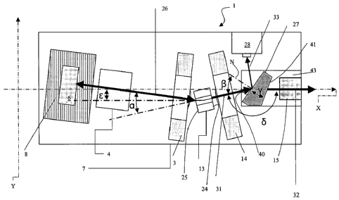
With now reference to fig. 2 where the external cavity laser module 1 of fig.1
is depicted in a
simplified top view and the beam directions within the laser module are
schematically shown.
For sake of clarity, the package enclosure and fibre pigtail 22 are not shown.
The incident angle
formed between an axis N normal to the first facet 40 surface and the incident
beam
propagating along the front facet output optical axis 31 is indicated with 13.
The Applicant has
found that the angle 13 should be preferably comprised between 42 and 50 by
taking into
account the finite size of the incident beam, the dimensions of the facet
itself and the
encumbrance of the photodiode.
The second facet 41 of the optical element 27 has an anti-reflective coating
and the reflectivity
is 0.2 % across the wavelengths range of interest. Preferably, said
wavelengths range of
interest is the C-band (1525 nm to 1565 nm) or the L- band (1570 nm to 1610
nm).
The incident beam propagating along the front facet output optical axis 31 and
impinging on the
multi-functional optical element 27 is then transmitted through the second
facet 41 and
deflected by given angle, which is a function on the angle y between the first
40 and the second
facet 41, the refractive index n of the optical element and the angle of
incidence of the beam.
14
CA 02732912 2010-09-28
WO 2008/119363
PCT/EP2007/002941
The beam 32 transmitted through the optic element 27 defines the output beam
of the laser
system, which propagates along the main longitudinal axis X of the optical
bench 10.
As shown in fig. 2, the main output optical axis X of the output beam forms a
first angle 6 with
respect to the direction of the beam propagating along the front facet output
optical axis 31. A
second angle s is formed between the main optical output axis X and the beam
emitted by the
back facet 25 of the gain medium 13 and propagating within the external cavity
along the intra-
cavity optical axis 26. The Applicant has noticed that, if the intra-cavity
optical axis 26 is tilted
with respect to the optical output axis X, an optimal space occupation within
the package 7 can
be achieved.
The angles E and 5 are determined by the incidence angle 13 on the multi-
functional element and
the angle 7 between the two facets 40, 41 of the optical element 27.
The material in which the multi-functional optical element 27 is realized is
preferably non
dispersive, to avoid a variation in the refractive index and thus a dependence
of the output
beam direction on the wavelength of the incident beam.
Preferably, the material in which the multi-functional optical element is made
is an E-F2 glass,
as described in the Hoya catalogue. The refraction index n of this material
varies as a function
of the wavelength of the incident light as plotted in the graph of fig. 7. As
shown, the refractive
index n changes from 1.5945 to 1.5938 in the operative range of 1520-1570 nm.
An angle a is defined as the angle formed between the two beams emerging from
the front and
back facet of the gain medium 13. This angle is generally fixed for a given
type. According to a
preferred embodiment of the invention, the gain medium is a semiconductor gain
chip having an
angle a of 19.5 . Any chip angle, as long as a 10 , can however be used in the
gain medium
13 comprised in the laser module 1 of the invention. Preferably, the angle a
is smaller than 35 .
The front facet output beam propagating along the front facet output optical
axis 31 is a
divergent beam. Applicant has considered the ranges of divergence angles of
the emitted
beams of some of the commercially available semiconductor laser chips, as
indicated in table 1.
Thus, the front facet output beam 31 generally exhibits a cross-sectional
elliptic shape. The
CA 02732912 2010-09-28
WO 2008/119363
PCT/EP2007/002941
mode field diameter (MFD) of the beam in cross section has a first value
(MFD(Y)) along the
direction parallel to the main direction of the optical bench 10 (Y direction)
and a second mode
field diameter (MFD(Z)) along a direction orthogonal to the bench (Z
direction).
Table 1
chip MFD(y) min (pm) MFD(y) max (pm) MFD(z) min (pm) MFD(z) max (pm)
#1 230 440 440 640
#2 280 460 360 580
#3 350 450 400 500
The multi-functional optical element 27 reshapes the beam propagating along
the front facet
output optical axis 31 by modifying the ratio between the two diameters.
Preferably, the element
is configured to modify the diameter of the beam along the Y axis while
leaving the MFD along
the Z axis substantially unaffected.
The variation in MFD(Y) induced by the multi-functional optical element 27
depends on the
angle 7 between the two facets 40, 41 and on /3.
For a selected angle 8. (in the example 8 = 167.5 ), the graph of fig. 4
reports computer
simulations showing the angle 7 as a function of the incidence angle p (left
scale; filled
diamonds connected with a dashed line).
From the curve plotted in fig. 4, the range of interest for the incidence
angle p results to
correspond to a range of the multi-functional optical element apertures, y,
from about 7 to 20 .
For different 8 values, curves that are qualitatively similar to the one of
fig. 4 can be obtained.
For values of angle 5 ranging from 150 to 170 , the Applicants have found
that the prism
aperture 7 should be selected between about 5 and 45 . In particular, if
8=150 , a suitable
range of angle 7 is comprised between about 30 and 45 , whereas for 8=170 , a
suitable range
of angle 7 is comprised between 5 and 15 .
16
CA 02732912 2010-09-28
WO 2008/119363
PCT/EP2007/002941
On the same graph of fig. 4, the curve with filled squares connected by a
solid line (right scale)
represents the corresponding increase of the MDF(Y) for each selected pair of
p and y angles.
In particular, the MDF(Y) percentage variation with respect to the mean MDF(Y)
of the chip
under consideration (chip 1 of table 1) is calculated.
All simulations are performed considering a laser module 1 comprising a
collimator
(schematically depicted in fig. 1 with reference number 17) accepting optical
beams having
MFD of 450um +1- 30 pm. An isolator 15 can be part of the collimator (not
shown in the figures)
or can be placed within the package, as illustrated in the embodiment of fig.
2.
The coupling efficiency between the output laser beam 32 and the fiber 22 is
maximised for a
circular cross-section of the beam. Therefore, an elliptic beam introduces
coupling losses in the
system. In fig. 5 several curves are plotted, each for a different value of
the p angle, showing the
"saved" losses, as detailed below. For each curve, a different multi-
functional optical element 27
is considered in the calculations, i.e. in each curve, the multi-functional
optical element has an
angle y between the facets given by the graph of fig. 4 corresponding to the
selected value of p.
Each curve represents the calculation, for different MFD(Y) of the input beam
incident on the
multi-functional optical element 27, of the losses "saved" due to the presence
of the multi-
functional optical element. In other words, the ordinate of the graph
represents the coupling
losses that should be added if the multi-functional optical element 27 were
not modifying the
incident beam cross section. The curves clearly shows that for the angles of
interest in the
preferred configuration of laser module, which is for 42 13 50 , and for
MDF(Y) values within
the range of interest (which is the range declared by the chip manufacturers,
the chip used in
the simulation is chip n. 1 of table 1), there is always a losses reduction
due to the presence of
the multi-functional optical element which modifies the MDF(Y) of the incident
beampropagating
along the front facet output optical axis 31.
In fig. 6 a graph is shown representing the variations in the angle 6 due to
variations of the
angle More in detail, the abscissa represents the variation from a
selected /3 = 48 (thus 13 =
48 is the zero in the abscissa). It is clear from the graph that a
misalignment in the optical
17
CA 02732912 2010-09-28
WO 2008/119363
PCT/EP2007/002941
element positioning, i.e. an erroneous positioning which results in a
different /3 angle with
respect to the selected one, results in a smaller variation in the angle 6
which is relevant for the
coupling losses. The multi-functional optical element thus relaxes the
tolorance requirements for
the alignment of the optical elements comprised in the laser cavity and in the
output optics.
18