Note: Descriptions are shown in the official language in which they were submitted.
CA 02732986 2011-01-28
WO 2010/014351 PCT/US2009/049660
-1-
PASSIVATED METAL CORE SUBSTRATE
AND PROCESS FOR PREPARING THE SAME
FIELD OF THE INVENTION
[0001] The present invention relates to electronic circuit assemblies, and
more
particularly, to circuit assemblies including metal core substrates, and the
fabrication thereof.
BACKGROUND OF THE INVENTION
[0002] Microelectronic circuit packages are prepared in various sizes. One
packaging
level includes semiconductor chips containing multiple microcircuits and/or
other
components. Such chips are usually made from semiconductors such as silicon,
and the like.
Intermediate package levels (i.e., "chip carriers") comprising multi-layer
substrates may
include a plurality of chips. Likewise, these intermediate package levels can
be attached to
larger scale circuit cards, motherboards, and the like. The intermediate
package levels serve
several purposes in the overall circuit assembly including structural support,
transitional
integration of the smaller scale circuits to larger scale boards, and the
dissipation of heat from
the circuit components. Substrates used in conventional intermediate package
levels have
included a variety of materials, for example, ceramics, fiberglass reinforced
polyepoxides,
and polyimides.
[0003] In order for the aforementioned substrates to have sufficient rigidity,
they
usually have to be used at thicknesses exceeding 100 microns to provide
structural support to
the circuit assembly. Also, the aforementioned substrates typically have
thermal coefficients
of expansion much different from that of the microelectronic chips attached to
them. As a
result, failure of the circuit assembly after repeated use is a risk due to
the failure of joints
between the layers of the assembly.
[0004] It would be desirable to provide a thin circuit assembly with improved
thermal
and structural properties that overcome the drawbacks of the prior art.
SUMMARY OF THE INVENTION
[0005] In a first aspect, the invention provides a substrate comprising an
iron-nickel
alloy core, a chromium conversion coating on at least a portion of the core,
and an insulating
coating on the chromium conversion coating.
[0006] In another aspect, the invention provides a method of making a
substrate
comprising: providing an iron-nickel alloy core, applying a hexavalent or
trivalent chromium
CA 02732986 2011-01-28
WO 2010/014351 PCT/US2009/049660
-2-
conversion coating on at least a portion of the core, and applying an
insulating coating on the
chromium conversion coating.
BRIEF DESCRIPTION OF THE DRAWINGS
[0007] FIG. 1 is a plan view of a substrate core that may be used in one
aspect of the
invention.
[0008] FIG. 2 is a cross-sectional view of the substrate core of FIG. 1, taken
along
line 2-2.
[0009] FIG. 3 is a plan view of the substrate core of FIG. 1, with a
passivation
coating.
[0010] FIG. 4 is a cross-sectional view of the substrate core of FIG. 3, taken
along
line 4-4.
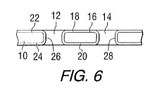
[0011] FIG. 5 is a plan view of the substrate of FIG. 3, with an insulating
coating.
[0012] FIG. 6 is a cross-sectional view of the substrate of FIG. 5, taken
along line 6-
6.
[0013] FIG. 7 is a plan view of the substrate of FIG. 5 with conductive tracks
on the
insulating coating.
[0014] FIG. 8 is a cross-sectional view of the substrate of FIG. 7, taken
along line 8-
8.
DETAILED DESCRIPTION OF THE INVENTION
[0015] In a first aspect, this invention relates to substrates having a metal
core that
may be coated with an organic insulating material. Such substrates may be used
in electronic
circuit packages.
[0016] FIG. 1 is a plan view of a substrate core 10 that may be used in one
aspect of
the invention. FIG. 2 is a cross-sectional view of the substrate core of FIG.
1 taken along line
2-2. In this example, the core includes a generally planar sheet of metal
alloy, which may or
may not include holes or vias, such as 12 and 14.
[0017] In some embodiments, the substrate core can have a thickness of about
10 to
400 microns, or more specifically about 20 to 200 microns. In specific
examples, the core
can have a minimum thickness of about 10 microns, about 20 microns, or about
30 microns.
The holes can have a uniform size and shape. When the holes are circular, the
diameter of
the holes can be as small as about 4 mil (101.6 microns). The holes may be
larger or smaller
CA 02732986 2011-01-28
WO 2010/014351 PCT/US2009/049660
-3-
as necessary, with the provision that the holes are large enough to
accommodate all the layers
applied in subsequent processing, without becoming obstructed.
[0018] In one example, the metal core can be an iron-nickel alloy, such as
INVAR,
(trademark owned by Imphy S. A., 168 Rue de Rivoli, Paris, France) comprising
approximately 64 weight percent iron and 36 weight percent nickel. This alloy
has a low
coefficient of thermal expansion, comparable to that of the silicon materials
used to fabricate
electronic devices (e.g., chips). This property is desirable in order to
prevent failure of
adhesive joints between successively larger or smaller scale layers of a chip
scale package,
due to thermal cycling in storage or normal use.
[0019] In previously known substrates that included an INVAR core, a layer of
copper metal has been applied to all surfaces of the INVAR core to provide
increased
conductivity. The layer of copper typically can have a thickness of from 1 to
20 microns.
However, it would be desirable to have substrates having an INVAR core that do
not include
a copper coating.
[0020] With an uncoated INVAR core, undesirable chemical changes at the
surface of
the iron-nickel core can result in the formation of corrosion products. These
chemical
changes can be accelerated at elevated temperatures. For example, corrosion
products may
be formed on an iron-nickel alloy core within 24 hours under the Autoclave
test conditions
set forth in the IPC-TM-650 protocol, even when the corrosion products do not
form under
standard ambient pressure corrosion testing after 2 weeks. It would be
desirable to minimize
the formation of corrosion products on the iron-nickel core.
[0021] In another example, the core material is KOVAR (trademark of Carpenter
Technology Corporation); an alloy of about 54% iron, 29% nickel, and 17%
cobalt. KOVAR
is a nickel-cobalt ferrous alloy designed to have a coefficient of thermal
expansion that is
compatible with other materials used in circuit assemblies.
[0022] In one aspect, this invention uses a chromium conversion treatment to
passivate an iron-nickel alloy substrate, which is then coated with a coating
of dielectric
material. The chromium conversion treatment is utilized as a passivating agent
for
preventing corrosion which can occur under the high pressure/high temperature
humid
environments normally seen in autoclave testing.
[0023] FIG. 3 is a plan view of the substrate core of FIG. 1, with a
passivation coating
16 applied to the surface of the core. FIG. 4 is a cross-sectional view of the
substrate core of
FIG. 3, taken along line 4-4.
CA 02732986 2011-01-28
WO 2010/014351 PCT/US2009/049660
-4-
[0024] In one aspect, this invention provides a method and apparatus using
trivalent
or hexavalent chromium as passivating agents for an INVAR or KOVAR core
substrate, that
can pass an adhesion peel test required by the IPC-TM-650 protocol. The IPC-TM-
650
protocol specifies a 96 hour autoclave test.
[0025] Chromium conversion passivation treatments have been applied to INVAR
and KOVAR metal cores in the following examples.
Example 1
Pretreatment of INVAR and KOVAR substrate cores in an Alodine process
using the following steps.
1) Ridolene 298 Cleaner: 130 F; 120 sec; immersion with agitation
2) Immersion Tap Rinse: ambient; 60 sec; with agitation
3) Spray tap rinse (water bottle)
4) DeOx 6/16 mixture: ambient; 150 sec; no agitation
5) Immersion Tap Rinse: ambient; 60 sec; with agitation
6) Spray tap water rinse (water bottle)
7a) Alodine 1000: ambient; 300 sec; no agitation
7b) Alodine 12005: ambient; 150 sec; no agitation
7c) Alodine 1600: ambient; 300 sec; no agitation
8) Immersion DIW Rinse: ambient; 60 sec; with agitation
9) Final spray rinse DIW (water bottle)
Steps 7a), 7b) and 7c) are optional alternative steps. If used, only one of
these
steps is used in a particular example.
Example 2
Pretreatment of INVAR and KOVAR substrate cores in a Metalast using the
following steps.
1) Metalast 1000 Cleaner: 120 F; 120 sec; immersion with agitation
2) Immersion DIW Rinse: ambient; 60 sec; with agitation
3) Spray DIW rinse (water bottle)
4) DeOx LNC: ambient; 180 sec; no agitation
5) Immersion DIW Rinse: ambient; 60 sec; with agitation
6) Spray DIW rinse (water bottle)
7) Metalast TCP: ambient; 300 sec; no agitation
8) Immersion DIW Rinse: ambient; 60 sec; with agitation
9) Final spray rinse DIW (water bottle)
CA 02732986 2011-01-28
WO 2010/014351 PCT/US2009/049660
-5-
[0026] In Examples 1 and 2, all deoxidizers-pretreatments were applied at room
temperature. The cleaner Ridolene 298 was applied via immersion at 130F for 2
min.
Ridolene 298 is available from Henkel Corporation. Metalast 1000 cleaner was
applied via
immersion at 120F for 2 min. Metalast 1000 is available from Metalast
International, Inc.
[0027] DeOx 6/16 is a deoxidizing treatment available from Henkel Corporation.
DeOx 6/16 serves as an acid etch solution. The etch rate can be controlled by
controlling the
acid fluoride concentration and/or the time for which the acid etch is applied
to the core.
Table 1 shows examples of how an Invar core thickness can be controlled by
controlling the
time for which it is exposed to an acid etch solution.
Table 1. Deoxidizer Effect on Invar vs. Time
Deox Time Invar Thickness
(min) ( m)
0 60
2 53
3 51
4 44
41
7 30
18
[0028] DeOx LNC is an aqueous deoxidizer available from Oakite.
[0029] Both hexavalent Cr and trivalent Cr treatments can be used to passivate
metal
surfaces. The reaction mechanism is different, hexavalent Cr is reduced to
trivalent Cr in an
electrolytic reaction with the substrate (substrate is oxidized). Trivalent Cr
treatments can
deposit their Cr onto the surface via metathesis (exchange of anions with the
metal surface).
In both cases the final product may contain an insoluble Cr (III) oxide which
acts as the
passivating layer. In both cases the treatments are typically referred to as
chromium
conversion coatings.
[0030] Alodine 1000, 1200S and 1600 are chrome conversion treatments available
from Henkel Corporation. Alodine 1000, 1200S and 1600 serve as passivation
solutions.
Metalast TCP-HF is an aqueous trivalent chromium pretreatment available from
Metalast
International, Inc.
[0031] FIG. 5 is a plan view of the substrate of FIG. 3, with an insulating
coating
applied to the passivating coating. FIG. 6 is a cross-sectional view of the
substrate of FIG. 5,
taken along line 6-6. First and second layers 18 and 20 of an insulating
material are
CA 02732986 2011-01-28
WO 2010/014351 PCT/US2009/049660
-6-
positioned on opposite sides (or surfaces) 22, 24 of the core. Additional
insulation 26 and 28
can be deposited on the walls of the openings 14 and 16.
[0032] The following examples illustrate the preparation of an
electrodeposition
coating and its use in coating passivated portions of the substrate core.
Example I
The following example describes the synthesis of the cationic binder used in
the electrodepositable coating bath described below. The binder was prepared
from the
following ingredients:
Ingredients Parts by Weight
(in grams)
MAZON® 1651' 150.0
EPON® 8802 755.3
Tetrabromo bisphenol A 694.9
TETRONIC® 150R13 0.2857
Aminopropyldiethanolamine 114.7
Diethanolamine 49.57
2-Butoxyethanol 382
EPON 880 48.3
Crosslinker4 1195
'A plasticizer, commercially available from BASF Corporation.
2An epoxy resin available from Hexion Specialty Chemicals.
3A surfactant, commercially available from BASF Corporation.
4A polyester prepared according to Example V of EP 0 012 463, and diluted to
90%
solids in 2-butoxyethanol.
[0033] The MAZON 1651, EPON 880, tetrabromo bisphenol A and TETRONIC
150R1 were charged to a 4-neck round bottom flask fitted with a stirrer,
temperature probe,
and Dean-Stark trap under a Nitrogen blanket. The mixture was heated to a
temperature of
70 C and stirred for 15 minutes. The heat source then was removed, and the
aminopropyldiethanolamine and diethanolamine were added. The reaction mixture
exothermed to a maximum temperature of 176 C after about 10 minutes. The
reaction was
allowed to cool to a temperature of 135 C over an hour, the 2-butoxyethanol
was added, and
the mixture was further cooled to 125 C. The mixture was then held at 125 C
for a total of
two hours from the peak exotherm. The second charge of EPON 880 and the
crosslinker
were added and the solution was stirred for 2.5 hours at 125 C. The reaction
mixture (3428
CA 02732986 2011-01-28
WO 2010/014351 PCT/US2009/049660
-7-
parts) was poured into a solution of sulfamic acid (49.5 parts) dissolved in
deionized water
(1287 parts) under strong agitation. After one hour agitation, an additional
amount of
deionized water (3970 parts) was added slowly, yielding a dispersion having a
30.2% non-
volatile content.
Example II
This example shows the preparation of an ungelled cationic soap used in the
synthesis of the microgel example shown below. The cationic soap was prepared
from the
following ingredients:
Ingredients Parts by Weight
(in grams)
EPON 828 1023
Bisphenol A-ethylene oxide adduct' 365
Bisphenol A 297
2-Butoxyethanol 187.2
Benzyldimethylamine 1.4
Benzyldimethylamine 3.0
Diketimine 182.3
N-methylethanolamine 85.2
Acetic Acid 105.9
Deionized water 1065.9
Deionized water 735.9
Deionized water 1156.4
Deionized water 867.3
'A 1/6 molar adduct of bisphenol A/ethylene oxide available from BASF
Surfactants.
2A 71 percent solution of the reaction product of diethylene triamine and
methylisobutyl
ketone in methylisobutyl ketone.
[0034] The EPON 828, bisphenol A-ethylene oxide adduct, bisphenol A and 2-
butoxyethanol were charged into a reaction vessel and heated under a nitrogen
atmosphere to
a temperature of 125 C. The first portion of the benzyldimethylamine was
added and the
reaction was allowed to exotherm to 180 C. During the exotherm when the
reaction reached
160 C, a one hour hold was begun. After the exotherm peak the resin was
allowed to cool
back to 160 C, continuing the hold. After the hold the reaction was cooled to
130 C, and
CA 02732986 2011-01-28
WO 2010/014351 PCT/US2009/049660
-8-
the second portion of benzyldimethylamine was added. The reaction was held at
130 C to an
extrapolated epoxy equivalent weight of 1070. At the expected epoxy equivalent
weight, the
diketimine and N-methylethanolamine were added in succession and the mixture
was allowed
to exotherm to approximately 150 C. At the peak exotherm, a one hour hold was
begun
while allowing the reaction to cool to 125 C. After the one hour hold the
resin was dispersed
into a solution of the acetic acid dissolved in the first portion of deionized
water. The
dispersion was later reduced with the second, third, and fourth portions of
deionized water.
The resulting cationic soap was vacuum stripped until the methylisobutyl
ketone level was
less than 0.05%.
Example III
This example shows the synthesis of a cationic microgel from the cationic
epoxy soap described above in Example II. The microgel was prepared from the
following
ingredients:
Ingredients Parts by Weight
(in grams)
Cationic soap of Example II 2517
Deionized water 443
EPON 828 (85% in methylisobutyl 66.4
ketone)
Methylisobutyl ketone 5.81
Deionized water 337
[0035] The deionized water was added to the cationic soap of Example 2, and
the
mixture was heated to 70 C under a nitrogen blanket. The EPON 828 solution
was added
over 15 minutes with good agitation. The methylisobutyl ketone was added as a
rinse, and
the mixture was held at 70 C for 45 minutes. The mixture was then heated to
90 C over 70
minutes and held at this temperature for 3 hours with good mixing. The
deionized water was
then added and the mixture was cooled yielding a microgel dispersion at 18.9%
non-volatile
content.
Electrodeposition Coating Bath and Coatings
Example A
CA 02732986 2011-01-28
WO 2010/014351 PCT/US2009/049660
-9-
This example shows the preparation of a blend used to prepare the coating
bath described below in Example C. The blend was prepared from the following
ingredients:
Raw Material Parts by Weight
(in grams)
Cationic Epoxy High MW with 1023.7
polyester x-linker
(Example 1)
Ethylene Glycol Monohexyl Ether 34.4
Microgel 344.3
(Example 3)
DI Water 2037.6
[0036] The electrodeposition resin of Example 1 was placed in a container
under slow
agitation. The ethylene glycol monohexyl ether was added to this resin slowly
under
agitation and stirred for 30 minutes. The deionized water was then added to
this mixture.
Example B
This example shows the preparation of a second blend used to prepare the
coating bath described below in Example C. The blend was prepared by adding
the following
catalyst to the blend of Example A:
Raw Material Parts by Weight
(in grams)
E6278' 13.0
'Catalyst paste, available from PPG Industries, Inc.
The above ingredients were mixed under low agitation for 30 minutes.
Example C
The second blend of Example B was added to the blend of Example A under
agitation. Approximately 1720 grams of permeate were removed from the coating
bath via
ultrafiltration, the permeate being replaced with deionized water. The final
pH and
conductivity of the ultrafiltered paint were 5.08 and 566 microsiemens
respectively. The
measured solids of the tank (1 hour at 110 C) was 9.43%.
Example D
The electrodepositable coating composition of Example C can be
electrophoretically applied to passivated substrate core from the
electrodeposition bath at a
temperature of 85 F for 45 to 240 seconds at 1.0 amps / 4" x 6" square
substrate depending
CA 02732986 2011-01-28
WO 2010/014351 PCT/US2009/049660
-10-
on desired coating thickness. The coating voltages can be, for example 150,
200, or 250
volts. The coating can then be cured (e.g., for 30 minutes at 240 Q.
[0037] The substrate can be circuitized to provide conductors on the
insulating
material. FIG. 7 is a plan view of the substrate of FIG. 5 with conductive
tracks 30, 32 on the
insulating coating. FIG. 8 is a cross-sectional view of the substrate of FIG.
7, taken along
line 8-8. The assembly is mechanically robust and provides for efficient
removal of heat
from the electronic devices that can be mounted on the substrate.
[0038] In another aspect, the invention encompasses a method of making an
electronic circuit assembly. The method comprises: (a) providing an iron-
nickel alloy core;
(b) applying a chromium conversion layer to at least a portion of the iron-
nickel alloy core;
and (c) applying a dielectric coating to a first surface of the chromium
conversion layer. In
this example, a metal core is formed first, and then any necessary
pretreatments, dielectric
coating application, sputtering, plating patterning, etc. are subsequently
applied.
[0039] The dielectric coating can be applied to the exposed surfaces of the
core to
form a conformal coating thereon. As used herein, a "conformal" film or
coating refers to a
film or coating having a substantially uniform thickness, which conforms to
the core
topography, including the surfaces within (but, preferably, not occluding)
holes in the core.
The dielectric coating film thickness can be, for example, between 5 and 50
microns. A
lower film thickness is desirable for a variety of reasons. For example, a
dielectric coating
having a low film thickness allows for smaller scale circuitry.
[0040] In another aspect, the invention provides a substrate including an iron-
nickel
alloy core having a plurality of holes or vias, a chromium conversion layer to
at least a
portion of the iron-nickel alloy core, and the holes or vias, and a dielectric
coating on at least
a portion of the chromium conversion layer and sidewalls of the holes or vias.
In some
embodiments, the core can have a thickness of about 10 to 400 microns, or more
specifically
about 20 to 200 microns. In specific examples, the core can have a minimum
thickness of
about 10 microns, about 20 microns, or about 30 microns. The core thickness
can be
controlled by controlling the acid fluoride concentration and/or the time for
which the acid
etch is applied to the core, as described above. In some examples, the ratio
of the diameter of
the holes to the thickness of the core can be about 2.5:1 or about 3:1. The
use of thin cores
allows the use of small holes having sidewalls that can be conformally coated
with the
described insulation coatings without plugging. For example, a 20 micron core
can include
holes as small as about 50 microns, or about 70 microns. In another example, a
30 micron
core can include holes as small as about 90 microns, or about 100 microns.
CA 02732986 2011-01-28
WO 2010/014351 PCT/US2009/049660
-11-
[0041] The conductors or contacts can be formed by chemical, mechanical or
laser
ablating or using masking technologies to prevent coating application at
selected areas or
otherwise removing portions of the dielectric coating in a predetermined
pattern to expose
sections of the electrically conductive core, and applying a layer of metal to
portions of the
dielectric coating to form conductors and contacts. Metallization of the
dielectric coating
layers can also be used to form contacts and conductors adjacent to the
surface of the
dielectric coating layers.
[0042] It should be understood that any of the processes of the present
invention can
include one or more additional steps without departing from the scope of the
inventor.
Likewise, the order in which the steps are performed may be changed as
necessary, without
departing from the scope of the invention.
[0043] Structures fabricated in accordance with the above examples passed
testing
required by the IPC-TM-650 protocol. The test samples included the core,
passivating
coating, and dielectric coating.
[0044] Other than in the operating examples, or where otherwise indicated, all
numbers expressing quantities of ingredients, reaction conditions and so forth
used in the
specification and claims are to be understood as being modified in all
instances by the term
"about." Accordingly, unless indicated to the contrary, the numerical
parameters set forth in
the following specification and attached claims are approximations that may
vary depending
upon the desired properties sought to be obtained by the present invention. At
the very least,
and not as an attempt to limit the application of the doctrine of equivalents
to the scope of the
claims, each numerical parameter should at least be construed in light of the
number of
reported significant digits and by applying ordinary rounding techniques.
[0045] Notwithstanding that the numerical ranges and parameters setting forth
the
broad scope of the invention are approximations, the numerical values set
forth in the specific
examples are reported as precisely as possible. Any numerical values, however,
inherently
contain certain errors necessarily resulting from the standard deviation found
in their
respective testing measurements.
[0046] Also, it should be understood that any numerical range recited herein
is
intended to include all sub-ranges subsumed therein. For example, a range of
"1 to 10" is
intended to include all sub-ranges between and including the recited minimum
value of 1 and
the recited maximum value of 10, that is, having a minimum value equal to or
greater than 1
and a maximum value of equal to or less than 10.
CA 02732986 2011-01-28
WO 2010/014351 PCT/US2009/049660
-12-
[0047] Whereas particular embodiments of this invention have been described
above
for purposes of illustration, it will be evident to those skilled in the art
that numerous
variations of the details of the present invention may be made without
departure from the
invention as defined in the appended claims.
[0048] As used in this description, unless indicated to the contrary, the
numerical
parameters are approximations that may vary depending upon the desired
properties sought to
be obtained by the present invention. Thus each numerical parameter should at
least be
construed in light of the number of reported significant digits and by
applying ordinary
rounding techniques, or by taking typically manufacturing tolerances into
account.
[0049] While the invention has been described in terms of several examples, it
will be
apparent to those skilled in the art that various changes can be made to the
described
examples without departing from the scope of the invention as set forth in the
following
claims.