Note: Descriptions are shown in the official language in which they were submitted.
CA 02733598 2011-02-08
WO 2010/019785 PCT/US2009/053729
Communications Connector with Multi-Stage Compensation
Background
[0001]There is a need to improve near-end crosstalk NEXT performance of
communications connectors at higher frequencies in a robust design that can be
relatively easily manufactured. This description is directed to a method of
improving NEXT performance in a communication connector by employing
specific capacitive and inductive couplings on a printed circuit board (PCB)
within
the connector.
Description of the Invention
[0002] Some embodiments of the present invention employ a PCB in a modular
jack assembly 10, which includes two-stage capacitor compensation/crosstalk
with time delay and a version of a "lattice network." More particularly, a PCB
designed according to embodiments of the present invention may be employed
as a rigid board 12 in a communication connector as shown in Fig. 1 and
schematically in Fig 2.
[0003] Other portions of the modular jack assembly 10 include the front
housing
14, a contact nose 16 which holds plug interface contacts that are
electrically
connected to the rigid board 12, insulation displacement contacts (IDCs) 18
which terminate wires of a communication cable (not shown) and also make
electrical contact with the rigid board 12, a rear housing 20, and a wiring
cap 22.
In a completed assembly, the plug interface contacts of the contact nose 16
and
the IDCs 18 are inserted via compliant pins into the rigid board 12. The front
housing 14 is clipped onto the rear housing 20, and the wiring cap 22 is
clipped
into the rear housing 20 thereby terminating wires of a communication cable at
the IDCs 18.
[0004]The self-inductive stubs of the present invention employ the distributed
electrical parameter of inductance per unit length of the circuit trace to
produce
the inductive elements. Although this configuration is modeled in the
schematics
below as a discrete inductor (which is appropriate as it has an equivalent
effect) it
is a distributed inductive component produced by the length of the traces as
CA 02733598 2011-02-08
WO 2010/019785 PCT/US2009/053729
opposed to turns of a wire coil, for example. In contrast, the capacitors
shown
herein are discrete capacitors although both the capacitors and the inductors
shown can be realized by discrete or distributed components, or as a
combination thereof. The lattice network generally includes a crosstalk
circuit
component and a compensation circuit component, each of which has a different
coupling rate versus frequency. A "crosstalk circuit component" is a circuit
component in which coupling occurs with the same polarity as crosstalk-
producing coupling within a plug, while a "compensation circuit component" is
a
circuit component in which coupling occurs in an opposite polarity to the
crosstalk
coupling that occurs within a plug.
[0005]The version of the lattice network used in embodiments of the present
invention utilizes a second self-inductive stub connected between a capacitor
and the second signal trace to the 2nd stage crosstalk network. Fig. 3
illustrates a
capacitor positioned between two inductors according to one embodiment of the
present invention. Positioning the capacitor between the two stubs improves
NEXT performance, relative to the opposite transmission direction (IDC to
PIC),
compared to putting the inductor on only one side of that capacitor, where the
inductance of the single inductor, L1, is about equal to L2 + L3 as shown in
Fig.
3. Additionally, the second stub shows improvements in return loss, also
relative
to using only a one-sided inductor.
[0006] Self-inductive stubs (shown in Fig. 3) as described herein refer to
traces
that are made specific lengths to take advantage of their self-inductance. The
term "stub" refers to the fact that these traces are not part of the main
current-
carrying path. They are stubs off of the current carrying path. Preferably, a
self-
inductive stub ends at a capacitor (i.e., there is no DC connection at the
endpoint
of the stubs). Current-carrying paths as described herein are traces that
allow a
DC current to flow between two points (such as the RJ45 plug and the
insulation
displacement contacts 18 (IDCs) in the jack).
[0007] EIA/TIA Category 6 ("CAT6") products generally have 8 wires that make
up 4 differential pairs. These wires are numbered numerically 1 through 8, and
2
CA 02733598 2011-02-08
WO 2010/019785 PCT/US2009/053729
the differential pairs are 45, 36, 12, and 78 (pairs 1, 2, 3, and 4,
respectively).
The layout of these wires within an RJ45 plug causes crosstalk between these
differential pairs that must be compensated for within a jack. Since there are
4
differential pairs, near end crosstalk (NEXT) can form between the six
different
pair combinations. These pair combinations are 45-36, 45-12, 45-78, 36-12, 36-
78, and 12-78.
[0008] Referring to Figs. 2, 4, and 5, the general design of a CAT6 jack
according
to one embodiment of the present invention uses time delay compensation for
pair combinations 45-36, 36-12, 36-78, and 45-12. Pair combinations 45-36, 36-
12, and 36-78 also make use of the lattice compensation technique. The type of
lattice network for pair combination 45-36 described here is shown in Fig. 6.
The
lattice network here utilizes the self-inductance on C34 and C56 to create a
"growing vector" in order to increase the overall NEXT bandwidth. Note that in
Fig. 6, the effect of the nose 16 is ignored.
[0009] This description takes into account the following:
= All capacitor dimensions given are referenced relative to the amount of
overlap occurring between the pads. According to some embodiments of
the present invention, one conductive pad of each capacitor is oversized 5
mils per side in each direction, for example, to help account for layer-to-
layer registration. The dimensions given herein are for the smaller layer.
According to one embodiment, capacitors are formed across a 4 mil core,
generally made of an FR4 material having a dielectric constant of
approximately 4.4.
= The capacitance and inductance values given here are for use with one
embodiment of an electrical connector. It is to be understood that the
principles of the present application can be applied using other
capacitance and inductance values. For example, different nose or IDC
designs, including different material selection, may make alternative
capacitance and inductance values beneficial.
3
CA 02733598 2011-02-08
WO 2010/019785 PCT/US2009/053729
= Aspects of the present disclosure may be applied to shielded and/or
punchdown-style connectors.
= The schematics shown for each description include only the intentional
capacitance added by design. For example, mutual inductance between
wires is purposely not shown for schematic clarity and due to the fact that
any mutual inductance that results from the design is not intentionally
used for compensation.
= These schematics do not show parasitic capacitances caused by the
geometry of the setup unless this parasitic capacitance is deemed
important to note (values greater than 0.1 pF). These values are noted,
but not labeled with reference characters.
= The schematics shown for each pair combination (Figs. 6-11) do not show
all connections since they are only showing two pairs at once. A full
schematic of rigid board 12 is shown in Fig. 2. Note that for pair
combinations 45-36, 36-12, and 36-78 the stub inductances are split
between some of the capacitors. These connections are not completely
shown in Figs. 6-11 and the nomenclature for the inductance reflects
which inductors are being used for which capacitors.
= The schematics shown attempt to approximate a "middle plug" which
refers to a plug whose crosstalk value is in the middle of the range of
crosstalk specified for that pair combination.
= All circuit board dimensions described in this RS are each individually
subject to change (estimates up to 20%). One reason for this is variability
of circuit board build tolerances from different circuit board manufacturers.
Different material or different processes may be used to manufacture the
circuit boards. Therefore, the performance of the circuit board may
change even though the artwork is identical due to the capacitance
changing. Another reason is to allow for design changes required to
compensate for different jack designs that might be needed.
4
CA 02733598 2011-02-08
WO 2010/019785 PCT/US2009/053729
Consequently, good engineering practice requires the ability to change the
area of overlap for the pad capacitors by the specification tolerance (about
20%). This change in area may be done on a capacitor-by-capacitor
basis; however, it is preferred for the overall board design (trace layout,
use of time delay, lattice) to remain constant even though capacitance
values may be changed according to some embodiments. Some variants
may only require changing the size of one or two capacitors (either smaller
or larger), and some may require changing the size of all capacitors.
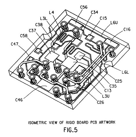
[0010] Referring to the Figures, and particularly to Figs. 4 and 5, which show
the
individual rigid PCB layers' artwork and combined rigid PCB artwork,
respectively, the PCB shown here has the following features. Dimensional
tolerances for capacitive pads are given for both dimensions.
1. Current carrying traces are routed between PIC vias and IDC vias with the
respective pin numbers. PIC vias refer to the vias where the compliant
pins from nose 16 interface with the rigid circuit board 12 in Fig. 1. The
IDC vias refer to the vias where the IDCs 18 interface with the rigid circuit
board 12 in Fig. 1.
2. Improved manufacturability of the circuit board that has been achieved
over previous CAT6 rigid circuit boards. This improved manufacturability
has been achieved through moving capacitors further away from the vias
so that they are less susceptible to manufacturing tolerances arising from
layer-to-layer registration and tolerances in the drilling (such as capacitors
C35 and C46 shown in Figs. 4 and 5). Additionally, square capacitors are
found to be less susceptible to manufacturing tolerances than rectangular
capacitors, so most capacitors on the board have been made square.
3. Crosstalk having the opposite polarity of the net crosstalk caused by the
plug for pair combination 45-78 is provided by pad capacitor C47
connected between the 4 and 7 PIC vias, and by pad capacitor C58
connected between IDC via 5 and pin PIC via 8. A schematic for pair
CA 02733598 2011-02-08
WO 2010/019785 PCT/US2009/053729
connection 45-78 is shown in Fig. 7. Pad capacitor C47 is sized 0.025" by
0.025" ( 20%), and pad capacitor C58 is sized 0.027" by 0.027" ( 20%).
4. Crosstalk compensation for pair combination 45-12 is achieved by using
the time delay model. A schematic for pair combination 45-12 is shown in
Fig. 8. Pad capacitor C25 has the opposite polarity of the net crosstalk
caused by the plug for pair combination 45-12 that connects between PIC
vias 2 and 5. Pad capacitor C15 has the same polarity of the net crosstalk
caused by the plug for pair combination 45-12 that connects between IDC
vias 1 and 5. C15 is time delayed from C25 by approximately 0.395"
(average distance between the 1, 2, 4, and 5 PIC vias to their respective
IDC vias). Pad capacitor C25 is 0.042" by 0.042" 20%, and pad
capacitor C15 is 0.033" by 0.033" 20%.
5. Crosstalk compensation for pair 45-36 is achieved by using the time delay
model and by a lattice network compensation technique. A schematic for
pair combination 45-36 is shown in Fig. 9. This time delay and lattice
network includes:
a. A pad capacitor C35 connected between PIC vias 3 and 5 having
the opposite polarity of the net crosstalk caused by the plug for pair
combination 45-36. The pad capacitor C35 is 0.068" by 0.068"
20%.
b. A pad capacitor C46 is connected between PIC vias 4 and 6 having
the opposite polarity of the net crosstalk caused by the plug for pair
combination 45-36. The pad capacitor C46 is 0.050" by 0.093"
20%.
c. A pad capacitor C34 is connected between PIC vias 3 and 4 having
the same polarity of the net crosstalk caused by the plug for pair
combination 45-36. The pad capacitor C34 is 0.046" by 0.046"
20%. This capacitor is time delayed from the C35 and C46
capacitors by approximately 0.39" (the average distance between
6
CA 02733598 2011-02-08
WO 2010/019785 PCT/US2009/053729
the 3, 4, 5, and 6 PIC vias to their respective IDC vias). The lattice
network is achieved here by the addition of self-inductive stub L3U
(approximately 0.9" in length) and another self-inductive stub L4
(approximately 0.5" in length).
d. A pad capacitor C56 having the same polarity of the net crosstalk
caused by the plug for pair combination 45-36 that connects
between IDC vias 5 and 6. The pad capacitor C56 is 0.0304" by
0.093" 20%. This capacitor is time delayed from the C35 and
C46 capacitors by approximately 0.39" (average distance between
the 3, 4, 5, and 6 PIC vias to their respective IDC vias). The lattice
network is achieved here by the addition of self-inductive stub L6U
and L6L (total length together of about 1.4"). Note that the self-
inductance L5 is ignored due to the fact the stub length is minimal.
6. Crosstalk compensation for pair combination 36-12 is achieved by using
the time delay model and by a lattice network compensation technique. A
schematic for pair combination 36-12 is shown in Fig. 10. This time delay
and lattice network includes:
a. A pad capacitor C13 having opposite polarity of the net crosstalk
caused by the plug for pair combination 36-12 that connects
between PIC vias 1 and 3. The pad capacitor C13 is 0.046" by
0.046" 20%.
b. A pad capacitor C26 having opposite polarity of the net crosstalk
caused by the plug for pair combination 36-12 that connects
between PIC vias 2 and 6. The pad capacitor C26 has an area of
0.00394 square inches 44%.
c. A pad capacitor C16 having the same polarity of the net crosstalk
caused by the plug for pair combination 36-12 that connects
between IDC vias 1 and 6. The pad capacitor C16 is 0.0335" by
0.0945" 20%. This capacitor is time delayed from the C13 and
7
CA 02733598 2011-02-08
WO 2010/019785 PCT/US2009/053729
C26 capacitors by approximately 0.38" (the average distance
between the 1, 2, 3, and 6 PIC vias to their respective IDC vias).
The lattice network is achieved here by the addition of a self-
inductive stub L6L (approximate length of 1 ") (this is the same 1-61
stub used by pad capacitor C56).
7. Crosstalk compensation for pair combination 36-78 is achieved by using
the time delay model and by a lattice network compensation technique. A
schematic for pair combination 36-78 is shown in Fig. 11. This time delay
and lattice network includes:
a. A pad capacitor C37 having opposite polarity of the net crosstalk
caused by the plug for pair combination 36-78 that connects
between PIC vias 3 and 7. The pad capacitor C37 is 0.058" by
0.058" 20%.
b. A pad capacitor C38 having the same polarity of the net crosstalk
caused by the plug for pair combination 36-78 that connects
between IDC via 3 and PIC via 8. The pad capacitor C38 is 0.034"
by 0.034" 20%. This capacitor is time delayed from the C37
capacitor by approximately 0.25" (average physical distance along
the trace between the 3, 6, 7, and 8 PIC vias to their respective IDC
vias). The lattice network is achieved here by the addition of self-
inductive stub L3U and L3L (total length together of about 1.1 ") (this
is the same L3U stub used by pad capacitor C34). Note that the
self-inductance L8 is ignored due to the fact the stub length is
minimal.
[0011]The self inductive stubs, along with corresponding capacitors (for
example, the L5-C56-L6 combination and L3-C34-L4 combination n Fig. 6), are
an LC circuit with a resonance effect, having a resonant frequency if
fo=1/(2rrAC). The selection of the inductance, L, and capacitance, C, values
is
generally a nonlinear multivariable optimization with multiple objective
functions
(NEXT, FEXT, return loss, etc.). Consequently, selection of a given L or C
value
8
CA 02733598 2011-02-08
WO 2010/019785 PCT/US2009/053729
is not made independent of other circuit considerations. Some of the
considerations for selecting a given L value include that if it is too low the
resonance point moves to a higher frequency and there may be no desired NEXT
improvement in the signal frequency operation range of interest; and if the
inductance is too high: a) the inductive traces can become to long to fit on a
typical rigid board, b) the resonance can move into the frequency operation
range of interest, possibly introducing deleterious effects; and c) there can
be a
degradation of return loss.
9