Note: Descriptions are shown in the official language in which they were submitted.
CA 02733765 2011-02-10
WO 2010/020753 PCT/GB2009/001966
HALO-HYDROCARBON POLYMER COATING
TECHNICAL FIELD
This disclosure relates generally to polymer coatings and, more specifically,
to
a halo-hydrocarbon polymer coating for electrical devices.
BACKGROUND
Many electrical devices comprise electrical components that are soldered to
printed circuit boards (PCBs). The metal surfaces on the electrical components
and
PCBs often oxidize or corrode before being soldered together. The oxidation or
corrosion of the metal surfaces may prevent strong solder joints from being
formed or
may reduce the lifetime of such joints. As a result, the electrical devices
may be
defective or may not function as long as desired.
SUMMARY
In some embodiments, a printed circuit board (PCB) comprises a substrate
comprising an insulating material. The PCB further comprises a plurality of
conductive tracks attached to at least one surface of the substrate. The PCB
further
comprises a coating deposited on the at least one surface of the substrate.
The coating
may cover at least a portion of the plurality of conductive tracks and may
comprise at
least one halo-hydrocarbon polymer. The PCB may further comprise at least one
conductive wire that is connected by a wire bond to at least one conductive
track,
wherein the wire bond is formed through the.coating without prior removal of
the
coating such that the wire bond abuts the coating.
In other embodiments, a PCB comprises a substrate comprising an insulating
material. The PCB further comprises a plurality of conductive tracks attached
to at
least one surface of the substrate. The PCB further comprises a multi-layer
coating
deposited on the at least one surface of the substrate. The multi-layer
coating (i)
covers at least a portion of the plurality of conductive tracks and (ii)
comprises at least
one layer formed of a halo-hydrocarbon polymer. The PCB further comprises at
least
CA 02733765 2011-02-10
WO 2010/020753 PCT/GB2009/001966
2
one electrical component connected by a solder joint to at least one
conductive track,
wherein the solder joint is soldered through the multi-layer coating such that
the
solder joint abuts the multi-layer coating.
In yet other embodiments, an apparatus comprises a substrate comprising an
insulating material. The apparatus further comprises a first contact attached
to at least
one surface of the substrate. The apparatus further comprises a coating
deposited on
at least one surface of the first contact. The coating may comprise at least
one halo-
hydrocarbon polymer such that the first contact is operable to conduct an
electrical
signal through the coating to a second contact without removal of the coating.
One or more embodiments may comprise a printed circuit board to which a
solder connection is to be made. The surface of said printed circuit board may
have a
multi-layer coating comprising one or more polymers. The polymers may be
selected
from halo-hydrocarbon polymers and non-halo-hydrocarbon polymers. The
thickness
of the multi-layer coating may be from 1 nm to 10 m.
One or more embodiments may comprise a printed circuit board to which a
solder connection is to be made. The surface of said printed circuit board may
have a
multi-layer coating comprising one or more polymers. According to certain
embodiments, there may be no solder, or essentially no solder, between said
coating
and conductive tracks of said printed circuit board.
One or more embodiments may comprise a printed circuit board to which a
solder connection is to be made. The surface of said printed circuit board may
have a
multi-layer coating comprising one or more polymers. The multi-layer coating
may
comprise one or more layers of discrete polymers.
One or more embodiments may comprise a printed circuit board to which a
solder connection is to be made. The surface of said printed circuit board may
have a
multi-layer coating comprising one or more polymers. The multi-layer coating
may
comprise graded layers of different polymers.
One or more embodiments may comprise a printed circuit board to which a
solder connection is to be made. The surface of said printed circuit board may
have a
multi-layer coating comprising one or more polymers. The multi-layer coating
may
comprise two or more layers.
CA 02733765 2011-02-10
WO 2010/020753 PCT/GB2009/001966
3
One or more embodiments may comprise a printed circuit board to which a
solder connection is to be made. The surface of said printed circuit board may
have a
multi-layer coating comprising one or more polymers. The first layer, which
may be
in contact with the surface of the printed circuit board, may comprise a non-
halo-
hydrocarbon polymer.
One or more embodiments may comprise a printed circuit board to which a
solder connection is to be made. The surface of said printed circuit board may
have a
multi-layer coating comprising one or more polymers. In some embodiments,
there
may be no, or essentially no, metal halide layer on the surface of the printed
circuit
board.
In some embodiments, a method of making a connection to a printed circuit
board having a multi-layer coating comprises applying solder, and optionally
flux, to
the printed circuit board at a temperature and for a time such that the solder
bonds to
the metal and the composition is locally dispersed and/or absorbed and/or
vaporised.
According to certain embodiments one or more factors are selected such that
(a) there
is good solder flow, (b) solder covers the substrate (typically a conductive
track or
pad) on the printed circuit board, and (c) a strong solder joint is generated.
The one or
more factors may comprise (a) the substrate characteristics, (b) the coating
characteristics, (c) the solder/flux characteristics, (d) the soldering
profile (including
time and temperature), (d) the process to disperse the coating, and (e) the
process to
control solder flow around the joint.
One or more embodiments may comprise a method of modifying the wetting
characteristics of a coating comprising one or more halo-hydrocarbon polymers
on a
printed circuit board by plasma etching, plasma activation, plasma
polymerisation and
coating, and/or liquid based chemical etching.
One or more embodiments may comprise a method of modifying the wetting
characteristics of a multilayer coating by plasma etching, plasma activation,
plasma
polymerisation and coating, and/or liquid based chemical etching.
In some embodiments, a printed circuit board comprises a substrate and
conductive tracks. The surfaces of said printed circuit board may be
completely or
substantially encapsulated with either (a) a coating of a composition
comprising one
CA 02733765 2011-02-10
WO 2010/020753 PCT/GB2009/001966
4
or more halo-hydrocarbon polymers, or (b) a multi-layer coating comprising one
or
more polymers selected from halo-hydrocarbon polymers and non-halo-hydrocarbon
polymers, at a thickness of I nm to 10 gm. According to certain embodiments,
the
substrate comprises a material that absorbs water or solvent based chemicals.
In some
embodiments, the substrate comprises epoxy resin bonded glass fabrics,
synthetic
resin bonded paper, phenolic cotton paper, cotton paper, epoxy, paper,
cardboard,
textiles, or natural or synthetic wood based materials.
In some embodiments, a method of preparing a printed circuit board
comprises: (a) providing a printed circuit board having an environmentally
exposed
surface, (b) cleaning the surface in a plasma chamber, using gases such as
hydrogen,
argon or nitrogen, and (c) applying to the surface a thickness of I nm to 10
m of a
composition comprising a halo-hydrocarbon polymer by plasma deposition, said
coating optionally following the 3D form of the printed circuit board.
In some embodiments, a method of preparing a printed circuit board
comprises: (a) providing a printed circuit board having an environmentally
exposed
surface, (b) cleaning the surface in a plasma chamber, using gases such as
hydrogen,
argon or nitrogen, (c) applying to the surface a thickness of 1 nm to 10 m of
a multi-
layer coating comprising one or more polymers by plasma deposition. The
polymers
may be selected from halo-hydrocarbon polymers and non-halo-hydrocarbon
polymers. The multi-layer coating may optionally follow the 3D form of the
printed
circuit board.
One or more embodiments may comprise using a composition comprising a
halo-hydrocarbon polymer as a flame-retardant coating for printed circuit
boards.
In some embodiments, a method of making a connection between a wire and a
substrate may use a wire bonding technique. The wire and/or the substrate may
be
coated with a composition that comprises one or more halo-hydrocarbon polymers
at
a thickness of from 1 nm to 2 m. In some embodiments, the wire bonding
technique
is ball/wedge bonding. In other embodiments, the wire bonding technique is
wedge/wedge bonding. According to certain embodiments, the wire comprises
gold,
aluminium, silver, copper, nickel, or iron. In some embodiments, the substrate
CA 02733765 2011-02-10
WO 2010/020753 PCT/GB2009/001966
comprises copper, gold, silver, aluminium, tin, conductive polymers, or
conductive
inks.
In some embodiments, a method of making a connection between a wire and a
substrate may use a wire bonding technique. In some embodiments, only the wire
is
5 coated with a composition that comprises one or more halo-hydrocarbon
polymers at
a thickness of from 1 nm to 2 m. In other embodiments, only the substrate is
coated
with a composition that comprises one or more halo-hydrocarbon polymers at a
thickness of from 1 nm to 2 m.
In some embodiments, a method of making a connection between a wire and a
substrate may use a wire bonding technique. The wire and/or the substrate may
be
coated with a composition that comprises one or more halo-hydrocarbon polymers
at
a thickness of from I Onm to 100nm.
In some embodiments, a method of making a connection between a wire and a
substrate may use a wire bonding technique. The wire and/or the substrate may
be
coated with a composition that comprises one or more halo-hydrocarbon
polymers. In
some embodiments, the halo-hydrocarbon polymer is a fluoro-hydrocarbon.
In some embodiments, a method of making a connection between a wire and a
substrate may use a wire bonding technique. The wire and/or the substrate may
be
coated with a composition that comprises one or more halo-hydrocarbon
polymers. In
some embodiments, the halo-hydrocarbon polymer coating remains intact after
wire
bonding except in the area where the connection is made. According to certain
embodiments, the halo-hydrocarbon polymer coating is removed and/or dispersed
by
the action of the wire bonding process, without the coating being removed in a
separate pre-processing step. In some embodiments, an additional coating
comprising
one or more halo-hydrocarbon polymers is applied after formation of the
connection.
In some embodiments, a halo-hydrocarbon polymer may be used to prevent
oxidation and/or corrosion of a wire and/or a substrate prior to formation of
a bond
between the wire and the substrate by a wire bonding technique. According to
certain
embodiments, a halo-hydrocarbon polymer may be used to allow formation of a
connection between a wire and a substrate under a non-inert atmosphere using a
wire
bonding technique.
CA 02733765 2011-02-10
WO 2010/020753 PCT/GB2009/001966
6
In some embodiments, a device comprises one or more contacts. At least one
of said contacts may be coated with a composition that comprises one or more
halo-
hydrocarbon polymers at a thickness of from I nm to 2 m.
In some embodiments, a device comprises an upper contact and a lower
contact. The device may be configured such that the upper contact and lower
contact
are capable of being brought into electrical contact with each other. The
upper and/or
lower contacts may be coated with a composition that comprises one or more
halo-
hydrocarbon polymers at a thickness of from 1 nm to 2 gm. In some embodiments,
the upper and lower contacts comprise stainless steel, silver, carbon, nickel,
gold, tin,
or alloys thereof. In some embodiments, the device is a keypad.
In some embodiments, a sensor device comprises one or more sensor elements
and each sensor element comprises a contact. The contacts may be coated with a
composition that comprises one or more halo-hydrocarbon polymers at a
thickness of
from I nm to 2 m. In some embodiments, the one or more sensor elements are
electrodes. In some embodiments, the contacts comprise carbon, conductive
inks,
and/or silver loaded epoxy.
In some embodiments, a device comprises one or more contacts. At least one
of said contacts may be coated with a composition that comprises one or more
halo-
hydrocarbon polymers at a thickness of from I Onm to I00nm.
In some embodiments, a device comprises one or more contacts. At least one
of said contacts may be coated with a composition that comprises one or more
halo-
hydrocarbon polymers. In some embodiments, the electrical conductivity of the
coating in the z-axis is higher than the electrical conductivity in the x-axis
and y-axis.
In some embodiments, the halo-hydrocarbon polymer coating provides
environmental
protection. In some embodiments, the electrical resistance of the coating can
be
optimised for different applications.
In some embodiments, a device comprises one or more contacts. At least one
of said contacts may be coated with a composition that comprises one or more
halo-
hydrocarbon polymers. A method for preparing the device may comprise
depositing
the halo-hydrocarbon polymer coating by plasma deposition. In some
embodiments,
the halo-hydrocarbon polymer is a fluoro-hydrocarbon.
CA 02733765 2011-02-10
WO 2010/020753 PCT/GB2009/001966
7
In some embodiments, a sensor element comprises a contact. The contact may
be coated with a composition that comprises one or more halo-hydrocarbon
polymers
at a thickness of from 1 nm to 2 m.
One or more embodiments may comprise a method of protecting one or more
upper and lower contacts in a device. The device may be configured such that
said
upper contact and lower contact are capable of being brought into electrical
contact
with each other. The method may comprise coating the contacts with a
composition
that comprises one or more halo-hydrocarbon polymers at a thickness of from I
nm to
2 m. In some embodiments, the coating is applied prior to manufacture of the
device.
One or more embodiments may comprise a method of protecting one or more
contacts in a sensor device. The method may comprise coating the contact pads
with
a composition that comprises one or more halo-hydrocarbon polymers at a
thickness
of from 1 nm to 2 m. In some embodiments, the coating is applied prior to
manufacture of the device. In some embodiments, the deposition technique is
plasma
deposition.
In some embodiments, a halo-hydrocarbon polymer may be used to coat a
surface or surfaces of contacts in a device comprising an upper contact and a
lower
contact. The device may be configured such that said upper contact and lower
contact
are capable of being brought into electrical contact with each other. In some
embodiments, a halo-hydrocarbon polymer may be used to coat a surface or
surfaces
of a contact in a sensor device comprising one or more sensor elements.
Applying the coating to a PCB or other device may provide several
advantages. Various embodiments may have none, some, or all of these
advantages.
One advantage is that the coating may prevent conductive tracks on a PCB from
oxidizing. A PCB is often stored for some period of time before electrical
components are soldered to the PCB. If the PCB is uncoated, the conductive
tracks
on the PCB may oxidize during storage. An oxidation layer on a conductive
track
may prevent or hinder the soldering of an electrical component to the
conductive
track. By applying the coating to the PCB prior to storage, a manufacturer may
prevent the conductive tracks on the PCB from oxidizing. By preventing
oxidation,
the coating may permit the formation of strong solder joints on the PCB.
CA 02733765 2011-02-10
WO 2010/020753 PCT/GB2009/001966
8
Another advantage is that the coating may allow an electrical component to be
soldered through the coating without the prior removal of the coating. The
coating
may comprise one or more halo-hydrocarbon polymers. In some embodiments, the
heat, solder, and/or flux applied during the soldering process may selectively
alter the
coating on the particular area of the PCB where the solder joint is to be
formed. In
some embodiments, the soldering process may remove the coating only in the
area of
the solder joint. Accordingly, once the solder joint is formed, the coating
may extend
up to (e.g., abut) the solder joint. As a result, a manufacturer may not need
to etch or
otherwise remove the coating prior to the soldering process. By eliminating
the need
for a separate etching or removal step, the coating may make the PCB assembly
process simpler, less expensive, and/or less time-consuming.
Another advantage is that the coating may prevent the corrosion of a PCB.
The coating may provide a barrier between a PCB and corrosive gases and/or
liquids.
In some embodiments, the coating may prevent liquids and/or moisture from
reaching
the substrate and/or conductive tracks of the PCB. The coating may prevent the
formation of dendrites that contribute to short circuits and/or leakage
between
contacts.
Another advantage is that the coating may exhibit conductivity along an axis
pointing into the plane of a coated surface (the "z-axis") while acting as an
insulator
along the axes parallel to the coated surface. Accordingly, the coating may be
applied
to a conductive contact without hindering the ability of such contact to
transmit an
electrical signal to a mating contact. Thus, in some embodiments, the coating
may
protect contacts from oxidation and/or corrosion without hindering the
conductivity of
the contacts.
Other advantages will be readily apparent to one skilled in the art from the
description and the appended claims.
CA 02733765 2011-02-10
WO 2010/020753 PCT/GB2009/001966
9
BRIEF DESCRIPTION OF THE DRAWINGS
For a more complete understanding of the present invention and for further
features and advantages, reference is now made to the following description,
taken in
conjunction with the accompanying drawings, in which:
FIGURES IA-C illustrate a printed circuit board (PCB), according to certain
embodiments;
FIGURE 2 illustrates the deposition of a coating on a PCB, according to
certain embodiments;
FIGURES 3A-B illustrate the soldering of an electrical component to
conductive tracks of PCB, according to certain embodiments;
FIGURE 4 illustrates a PCB comprising a multi-layer coating, according to
certain embodiments;
FIGURE 5 illustrates a PCB comprising a multi-layer coating selectively
applied to particular regions of the PCB, according to certain embodiments;
FIGURES 6A-B illustrate a keypad comprising contacts that are coated with a
coating, according to certain embodiments;
FIGURE 7 is a graph illustrating the z-axis conductivity of example coatings
having various thicknesses, according to certain embodiments;
FIGURE 8 illustrates a measuring device comprising a sensor having coated
contacts, according to certain embodiments;
FIGURE 9 illustrates a wire bond that is formed through a coating, according
to certain embodiments;
FIGURE IOA illustrates a microscope image of ball bonds formed between
uncoated wires and a coated contact surface, according to certain embodiments;
FIGURE 10B illustrates a microscope image of a section view of a ball bond
between an uncoated wire and a coated contact surface, according to certain
embodiments;
FIGURE 11A illustrates a microscope image of wedge bonds between
uncoated wires and a coated contact surface, according to certain embodiments;
FIGURE 11B illustrates a microscope image of a section view of a wedge
bond between a coated wire and a coated contact surface; and
CA 02733765 2011-02-10
WO 2010/020753 PCT/GB2009/001966
FIGURE 12 illustrates a PCB having a ball bond and a wedge bond, according
to certain embodiments.
DETAILED DESCRIPTION OF THE DRAWINGS
5 FIGURE IA illustrates a printed circuit board (PCB) 10, according to certain
embodiments. PCB 10 may mechanically support and/or electrically connect one
or
more electrical components 12 associated with an electrical circuit. PCB 10
may
comprise a substrate 14, one or more conductive tracks 16, a coating 18, and
one or
more electrical components 12.
10 Substrate 14 in PCB 10 may comprise one or more boards that mechanically
support elements of a circuit. For example, conductive tracks 16 and/or
electrical
components 12 may be affixed to at least one surface of substrate 14.
Substrate 14
may comprise any suitable insulating material that prevents substrate 14 from
shorting
the circuit of PCB 10. In some embodiments, substrate 14 in PCB 10 comprises
an
epoxy laminate material, a synthetic resin bonded paper, an epoxy resin bonded
glass
fabric (ERBGH), a composite epoxy material (CEM), a phenolic cotton paper,
and/or
any other suitable type and/or combination of insulating material. According
to
certain embodiments, substrate 14 comprises paper, cardboard, natural and/or
synthetic wood based materials, and/or other suitable textiles. In some
embodiments,
substrate 14 comprises a flame retardant material such as, for example, Flame
Retardant 2 (FR-2) and/or Flame Retardant 4 (FR-4). Substrate 14 in PCB 10 may
comprise a single layer of an insulating material or multiple layers of the
same or
different insulating materials with or without conductive tracks 16 on any
layer.
One or more conductive tracks 16 may be affixed to at least one surface of
substrate 14. Conductive track 16 is generally operable to conduct electrical
signals
between two or more components of the circuit of PCB 10. Thus, conductive
track 16
may function as a signal trace and/or wire for conducting signals. In some
embodiments, conductive tracks 16 comprise regions referred to as contact
pads. A
contact pad of conductive track 16 may be configured to support and/or connect
with
electrical component 12. Conductive track 16 may comprise any suitable
conductive
material such as, for example, gold, tungsten, copper, silver, aluminium,
and/or tin.
CA 02733765 2011-02-10
WO 2010/020753 PCT/GB2009/001966
11
In some embodiments, conductive track 16 may comprise one or more conductive
polymers and/or conductive inks.
Conductive track 16 may be formed on substrate 14 of PCB 10 using any
suitable technique. In some embodiments, conductive track 16 may be formed on
substrate 14 using a "subtractive" technique. For example, a layer of metal
(e.g.,
copper foil, aluminium foil, etc.) may be bonded to a surface of substrate 14
and then
the unwanted portions of the metal layer may be removed, leaving the desired
conductive tracks 16. The unwanted portions of the metal layer may be removed
from substrate 14 by chemical etching, photo-etching, milling, and/or any
suitable
technique. In other embodiments, conductive tracks 16 may be formed on
substrate
14 using an "additive" technique such as, for example, electroplating,
deposition
using a reverse mask, and/or any geometrically controlled deposition process.
In some embodiments, coating 18 may be deposited over one or more
conductive tracks 16 on substrate 14 of PCB 10. Coating 18 may protect
conductive
tracks 16 from oxidation, corrosion, and/or other environmental hazards (e.g.,
swelling caused by liquids and/or moisture). In some embodiments, coating 18
is
deposited over conductive tracks 16 on substrate 14 prior to soldering
electrical
components 12 to conductive tracks 16 of PCB 10. Thus, there may be no solder,
or
essentially no solder, at an interface 20 between coating 18 and conductive
tracks 16
of PCB 10. Coating 18 may permit electrical components 12 to be selectively
soldered through coating 18 to conductive tracks 16 without prior removal of
coating
18. In addition, or alternatively, coating 18 may permit wires to be wire
bonded
through coating 18 to conductive tracks 16 without prior removal of coating
18. In
addition, or alternatively, coating 18 may exhibit low resistance and/or
impedance
along the z-axis 22 (i.e., axis pointing into the surface of PCB 10 to which
conductive
tracks 16 are affixed) such that an electrical signal and/or current may be
conducted
through coating 18 between conductive track 16 and electrical component 12 of
PCB
10. In this context, the term "current" may refer to the flow of electric
charge and the
term "signal" may refer to a time-varying and/or spatial-varying electric
quantity
(e.g., voltage, current, or field strength whose modulation represents coded
CA 02733765 2011-02-10
WO 2010/020753 PCT/GB2009/001966
12
information). The signal may be any suitable type of signal such as, for
example, a
field induced signal or a current induced signal.
Coating 18 may comprise any suitable material that protects conductive tracks
16 from oxidation and/or corrosion. In some embodiments, coating 18 comprises
one
or more halo-hydrocarbon polymer materials. The term "polymer" may refer to
polymers formed in-situ from single and/or multiple monomers, linear,
branched,
grafted, and/or crosslinked copolymers, oligomers, multipolymers, multimonomer
polymers, polymer mixtures, blends and/or alloys of polymers, grafted
copolymers,
and/or interpenetrating networks of polymers (IPNs).
The term "halo-hydrocarbon polymer" may refer to polymers with a straight
or branched chain or ring carbon structure with zero, one, two, or three
halogen atoms
bound to each carbon atom in the structure. The halogen atoms in the halo-
hydrocarbon polymer may be fluorine, chlorine, bromine, and/or iodine.
Preferably,
the halo-hydrocarbon polymer is a fluoro-hydrocarbon polymer, a chloro-
hydrocarbon
polymer, or a fluoro-chloro-hydrocarbon polymer wherein zero, one, two, or
three
fluorine or chlorine atoms are bonded to each carbon atom in the chain. In
some
embodiments, the chain may be conjugated or highly conjugated or have extended
conjugated chains, rings, and/or branches.
The halogen atoms in the halo-hydrocarbon polymer in coating 18 could be
the same halogen atoms (e.g., fluorine) or a mixture of halogen atoms (e.g.,
fluorine
and chlorine). The term "halo-hydrocarbon polymer" as used herein may include
polymers that comprise one or more unsaturated groups, such as carbon-carbon
double and/or triple bonds, and/or polymers that comprise one or more
heteroatoms
(atoms which are not carbon, hydrogen, or a halogen) such as, for example,
nitrogen,
sulphur, and/or oxygen. Preferably, the halo-hydrocarbon polymer in coating 18
comprises less than five percent heteroatoms as a proportion of the total
number of
atoms in the polymer. The halo-hydrocarbon polymer may have any suitable
molecular weight. The molecular weight of the halo-hydrocarbon polymer may be
selected according to the desired functionality of coating 18. In a preferred
embodiment, the molecular weight of the halo-hydrocarbon polymer in coating 18
is
greater than 500 amu. The halo-hydrocarbon polymer chains in coating 18 may be
CA 02733765 2011-02-10
WO 2010/020753 PCT/GB2009/001966
13
straight or branched. In some embodiments, there is crosslinking between the
polymer chains in coating 18.
Examples of preferred halo-hydrocarbon polymers include:
^ Polytetrafluoroethylene (PTFE), PTFE type material, fluorinated-
hydrocarbons, chlorinated-fluorinated-hydrocarbons, halogenated-
hydrocarbons, and halo-hydrocarbons as well as copolymers, oligomers,
multipolymers, multimonomer polymers, polymer mixtures, interpenetrating
polymer networks (IPNs), blends, alloys, branched chain polymers, grafted
copolymers, and cross-linked variants of these materials. In a preferred
embodiment, the halo-hydrocarbon polymer in coating 18 is a
polytetrafluoroethylene (PTFE) type material and, in particular, modified or
unmodified polytetrafluoroethylene (PTFE).
^ Polychlorotrifluoroethylene (PCTFE) and copolymers, oligomers,
multipolymers, multimonomer polymers, polymer mixtures, interpenetrating
polymer networks (IPNs), blends, alloys, branched chain polymers, grafted
copolymers, and cross-linked variants of these materials.
^ Ethylene copolymer of polychlorotrifluoroethylene (EPCTFE) and
copolymers, oligomers, multipolymers, multimonomer polymers, polymer
mixtures, interpenetrating polymer networks (IPNs), blends, alloys, branched
chain polymers, grafted copolymers, and cross-linked variants of these
materials.
^ Copolymer of ethylene and tetrafluoroethylene (ETFE); copolymer of
tetrafluoroethylene and hexafluoropropylene (FEP); copolymer of
tetrafluoroethylene and perfluorovinyl ether (PFA); polymer of
vinylidenefluoride (PVDF); copolymer of tetrafluoroethylene,
hexafluoropropylene and vinylidenefluoride (THV); copolymer of vinylidene
fluoride and hexafluoropropylene (PVDFHFP); copolymer of
tetrafluoroethylene and perfluoromethylvinylether (MFA); copolymer of
ethylene, tetrafluoroethylene and hexafluoropropylene (EFEP); copolymer of
hexfluoropropylene, tetrafluoroethylene and ethylene (HTE); copolymer of
vinylidene fluoride and chlorotrifluoroethylene; and/or other fluoroplastics
CA 02733765 2011-02-10
WO 2010/020753 PCT/GB2009/001966
14
including copolymers, oligomers, multipolymers, multimonomer polymers,
polymer mixtures, interpenetrating polymer networks (IPNs), blends, alloys,
branched chain polymers, grafted copolymers, and cross-linked variants of
these materials.
Coating 18 on PCB 10 may comprise a single layer or multiple layers of halo-
hydrocarbon polymers. In some embodiments, coating 18 comprises at least one
layer
of halo-hydrocarbon polymers and at least one layer of a metal halide (e.g.,
metal
fluoride) on a conductive surface. Coating 18 may have any suitable thickness
24. In
some embodiments, thickness 24 of coating 18 may be from one nanometers (nm)
to
ten micrometers (gm). In other embodiments, thickness 24 of coating 18 may be
from
one nm to two m. In yet other embodiments, thickness 24 of coating 18 may be
from one nm to five hundred nm. In yet other embodiments, thickness 24 of
coating
18 may be from three nm to five hundred nm. In yet other embodiments,
thickness 24
of coating 18 may be from ten nm to five hundred nm. In yet other embodiments,
thickness 24 of coating 18 may be from ten nm to two hundred and fifty nm. In
yet
other embodiments, thickness 24 of coating 18 may be from ten nm to thirty nm.
In
yet other embodiments, coating 18 is a monolayer of a halo-hydrocarbon polymer
(having thickness 24 of a few angstroms (A)). In a preferred embodiment,
thickness
24 of coating 18 is from ten nm to one hundred nm in various gradients, with
one
hundred nm being a preferred thickness 24. In some embodiments, coating 18 may
be
deposited on substrate 14 and conductive tracks 16 such that an exposed
surface of
coating 18 is substantially flat (as illustrated in FIGURE IA). In other
embodiments,
coating 18 may be deposited on substrate 14 and conductive tracks 16 such that
an
exposed surface of coating 18 is not flat but instead conforms to a three-
dimensional
surface of substrate 14 and conductive tracks 16 (as illustrated in FIGURE
1B).
In some embodiments, coating 18 may be deposited on conductive tracks 16
and/or substrate 14 as a continuous film. According to certain embodiments,
the
continuous film may be substantially free of pores such as, for example,
voids, cracks,
holes, and/or defects. In some embodiments, the porosity of coating 18 may be
configured to provide the desired permeability of coating 18. For example,
altering
the porosity of coating 18 may increase or decrease the permeability of
coating 18 to
CA 02733765 2011-02-10
WO 2010/020753 PCT/GB2009/001966
liquids, chemicals, gases, and/or solder. The alteration of the porosity of
coating 18
may be a physical, chemical, and/or structural change to the polymer(s) in
coating 18.
In some embodiments, changing the surface energy of coating 18 may change the
permeability of coating 18 to liquids, chemicals, gases, and/or solder. By
controlling
5 the relative surface energy of coating 18 to the surface energy of the
penetrating liquid
and/or gas, one may increase or decrease the permeability of coating 18.
Controlling
the permeability of coating 18 to water and/or other solvents may be
especially
desirable for PCBs 10 that are subjected to liquid environments (e.g., aqueous
environments) and/or to solvents (e.g., during the cleaning process while
10 manufacturing PCB 10). In some embodiments, the porosity of coating 18 may
be
configured such that coating 18 is selectively permeable to particular
material(s) but
not to other material(s). For example, coating 18 may be substantially
impermeable
to water while being permeable to other liquids.
In some embodiments, coating 18 may comprise multiple layers with a thin,
15 exposed layer (e.g., upper layer) that is substantially free of pores.
Thus, the exposed
layer of coating 18 may be substantially impermeable to gases, moisture,
and/or
liquids. In such embodiments, the concealed layer(s) of coating 18 (e.g., the
layer(s)
between conductive tracks 16 and the exposed layer of coating 18) may comprise
pores that permit the concealed layer(s) to conduct an electrical current
and/or signal.
According to certain embodiments, coating 18 may exhibit a self-healing
property. In some embodiments, this self-healing property may be a mechanical
property that allows coating 18 to move and/or compress in response to a
physical
force and then, once the force subsides, to return to its original structure
and/or shape.
In other embodiments, this self-healing property may permit electrical self-
healing of
coating 18. When a physical and/or electrical force is applied to a particular
area of a
coated substrate 14, coating 18 on the particular area of substrate 14 may be
compressed and/or otherwise altered. When the physical and/or electrical force
subsides, coating 18 on the particular area may "heal" and/or otherwise
reorganize to
cover the particular area of substrate 14.
Coating 18 may exhibit relatively low gaseous permeability, thus providing a
significant barrier to gaseous permeation and avoiding gaseous corrosion
and/or
CA 02733765 2011-02-10
WO 2010/020753 PCT/GB2009/001966
16
oxidation through coating 18 to conductive tracks 16. In some embodiments,
electrical components 12 may be selectively soldered through coating 18
without
prior removal of coating 18. Solder joints 26 achieved by soldering through
coating
18 may be strong in comparison to solder joints 26 associated with other
currently
available surface finishes. In some embodiments, coating 18 may be configured
to
withstand multiple heat cycles. Coating 18 may exhibit chemical resistance to
corrosive gases, liquids, and/or salt solutions such as, for example,
environmental
pollutants. In some embodiments, coating 18 may exhibit low surface energy
and/or
"wettability." The materials in coating 18 and/or the method of depositing
coating 18
may be configured to control the relative wettability of coating 18. Coating
18 may
be a stable inert material at normal device temperatures (e.g., at temperature
ranges
where PCB 10 may be used). Coating 18 may exhibit good mechanical properties
such as, for example, abrasion resistance and/or adhesion to PCB materials. In
some
embodiments, coating 18 may exhibit improved electrostatic protection. Coating
18
may have relatively low liquid and salt solution permeability, thus avoiding
liquid
corrosion through coating 18. According to certain embodiment, coating 18 may
generally be environmentally beneficial compared to existing finishes.
Coating 18 on PCB 10 may be continuous, substantially continuous, or non-
continuous over one or more surfaces of PCB 10. In some embodiments, coating
18
is continuous or substantially continuous over surfaces to be soldered and non-
soldering surfaces between or adjacent to them. According to certain
embodiments,
coating 18 is continuous or substantially continuous over substantially all
exposed
and/or vulnerable surfaces of PCB 10. While a substantially continuous coating
18
may be preferred to protect PCB 10 from harmful environments, a non-continuous
coating 18 may be preferred for other purposes.
In some embodiments, PCB 10 comprises one or more electrical components
12 that are affixed through coating 18 to conductive tracks 16 on substrate
14.
Electrical component 12 may be any suitable circuit element of PCB 10. For
example, electrical component 12 may be a resistor, transistor, diode,
amplifier,
oscillator, and/or any suitable element. In some embodiments, electrical
component
12 comprises one or more leads configured to be affixed to a portion of
conductive
CA 02733765 2011-02-10
WO 2010/020753 PCT/GB2009/001966
17
track 16 on substrate 14 of PCB 10. Any suitable number and/or combination of
electrical components 12 may be affixed to PCB 10.
Electrical components 12 may be affixed to conductive tracks 16 on substrate
14 using any suitable technique. In some embodiments, electrical component 12
may
be connected to conductive track 16 by welding, laser-enhanced welding,
ultrasonic
welding, and/or use of conductive adhesives. According to certain embodiments,
electrical component 12 may be soldered through coating 18 to conductive track
16
on substrate 14 without the prior removal of coating 18. The solder connection
between electrical component 12 and conductive track 16 may be referred to as
solder
joint 26. Prior to the formation of solder joint 26, coating 18 may protect
conductive
tracks 16 from oxidation and/or corrosion. In some embodiments, because solder
joint 26 may be formed through coating 18 without the prior removal of coating
18,
coating 18 may abut solder joint 26. By abutting solder joint 26, coating 18
may
protect conductive tracks 16 from oxidation and/or corrosion even after
electrical
components 12 are soldered to PCB 10.
Solder joint 26 between electrical component 12 and conductive track 16 may
be formed using leaded solder or lead-free solder. In some embodiments,
soldering
through coating 18 does not reduce the strength of solder joint 26, as might
be
expected. Indeed, in some embodiments, solder joint 26 formed by soldering
through
coating 18 may be stronger than a solder joint on alternative surface
finishes. Solder
joint 26 may be formed according to any suitable technique. In some
embodiments, a
flux (not illustrated) may be used to form solder joint 26. In other
embodiments, a
soldering process that uses heat alone (e.g., laser soldering) could be used
to
selectively form solder joint 26. In yet other embodiments, solder joint 26
may be
formed by wave soldering, which may entail selective fluxing.
As noted above, solder joint 26 may be formed through coating 18 between
electrical component 12 and conductive track 16. In this context, the phrase
"formed
through" may refer to the formation of solder joint 26 without the prior
removal of
coating 18 from conductive track 16. Thus, conductive track 16 may be coated
with
coating 16 and then, without first removing coating 18 from conductive track
16, one
or more electrical components 12 may be soldered to conductive track 16. The
CA 02733765 2011-02-10
WO 2010/020753 PCT/GB2009/001966
18
soldering process may selectively alter coating 18 and may form solder joint
26
between electrical component 12 and conductive track 16. Thus, the phrase
"formed
through" may refer to the formation of solder joint 26 without the prior
removal of
coating 18 from conductive track 16.
As noted above, because solder joint 26 may be formed through coating 18
without the prior removal of coating 18, solder joint 26 may abut coating 18.
In this
context, the term "abutting" may refer to one or more edges of solder joint 26
directly
touching, substantially touching, and/or being in substantial proximity to one
or more
edges of coating 18. Thus, solder joint 26 may border on the portion of
coating 18
that is not selectively altered (e.g., removed) by the soldering process. In
some
embodiments, solder joint 26 may abut coating 18 in a single dimension or in
multiple
dimensions. For example, as illustrated in FIGURE IA, solder joint 26 may abut
coating in the x-axis and/or y-axis direction but not in the z-axis direction.
PCB 10 comprising coating 18 may provide advantages over uncoated PCBs
10.. Coating 18 may provide none, some, or all of the following advantages.
One
advantage is that, in some embodiments, coating 18 may protect PCB 10 from
oxidizing and/or corroding while being stored. Once conductive tracks 16 are
formed
on substrate 14, manufacturers may store PCB 10 for variable periods of time,
potentially up to several months or years, prior to attachment of electrical
components
12. If left uncoated, materials in conductive tracks 16 (e.g., copper) may
oxidize in
air, resulting in a layer of oxide and/or tarnish forming on conductive tracks
16.
Because traditional PCBs 10 lack coating 18, conductive tracks 16 on
traditional
PCBs 10 may oxidize and/or corrode during storage. The longer an uncoated PCB
10
is stored, the more oxidation may occur. An oxide or corrosion layer on
uncoated
conductive tracks 16 may hinder the formation of strong solder joints 26. In
particular, the presence of an oxide or corrosion layer on conductive tracks
16 may
result (i) in weak joints with low mechanical strength, (ii) in "dry joints"
that have a
tendency to fail during operation of the device, (iii) in a joint that fails
to make
electrical contact altogether, and/or (iv) in the failure of PCB 10 (e.g.,
failure or
degradation between conductive tracks 16). In contrast, if coating 18 is
applied to
PCB 10, coating 18 may prevent oxidation and/or corrosion of conductive tracks
16
CA 02733765 2011-02-10
WO 2010/020753 PCT/GB2009/001966
19
on PCB 10 during long-term storage (e.g., months or years), thus permitting
strong
solder joints 26 to be formed on conductive tracks 16 after storage. In
embodiments
where coating 18 is applied to metal and/or polymer based electronics, coating
18
comprising halo-hydrocarbon polymers may prevent swelling of conductors and/or
devices.
Another advantage is that, in some embodiments, coating 18 comprising halo-
hydrocarbon polymers may not be as expensive and/or environmentally harmful as
traditional finishes. Manufacturers have applied metal finishes (e.g., tin,
silver,
nickel, and/or gold) to areas where soldering would be required. The processes
for
applying these finishes are time consuming, require additional metals to be
used, and
pose environmental problems. These finishes and processes may be expensive
and/or
pose health risks. In some cases, manufacturers have used finishes comprising
organic compounds such as benzimidazoles and particles of solder-wettable
metals or
solder. These organic finishes, however, often do not survive multiple heat
cycles and
exhibit a relatively short storage life before processing. Thus, the
traditional finishes
used by manufacturers are generally expensive, time consuming, and/or require
extra
steps in the manufacturing process. The traditional finishes have also
depleted non-
renewable resources such as precious metals. In contrast to the traditional
finishes,
coating 18 comprising a halo-hydrocarbon polymer may represent a less
expensive
and/or higher performance coating 18 that prevents oxidation of conductive
tracks 16
prior to attaching electrical components 12 by soldering.
Another advantage is that, in some embodiments, coating 18 comprising halo-
hydrocarbon polymer may prevent the formation of dendrites between solder
joints
26. Dendrites of metal compounds have been observed to form in gaps between
solder joints 26 on uncoated PCBs 10. Dendrites may cause short circuits and
electrical leakage between connectors, resulting in failure of PCB 10. In
particular,
dendrites may form when moisture reaches an uncoated substrate 14 and/or
conductive track 16 and generates metal ions, which are then redistributed by
electromigration in the presence of an electromagnetic field. Dendrites may
represent
metallic growths that are caused by electromigration and form fern-like
patterns along
surfaces. In embodiments where coating 18 is applied prior to the formation of
solder
CA 02733765 2011-02-10
WO 2010/020753 PCT/GB2009/001966
joint 26, coating may not prevent liquids from reaching solder joint 26.
However, in
such embodiments, coating 18 may prevent moisture from reaching substrate 14
and/or conductive tracks 16 of PCB (which is where dendrites may tend to form
by
ionic dissolution). Thus, coating 18 may protect PCB 10 against the formation
of
5 dendrites by (i) preventing moisture from reaching substrate 14 and/or
conductive
tracks 16, and/or (ii) by providing a physical barrier between conductors on
PCB 10.
In addition, or alternatively, because dendrite materials may have low
adhesion to
coating 18, coating 18 may reduce the formation of dendrites between
conductive
tracks 16 and/or electrical components 12 on PCB 10. In addition, or
alternatively,
10 coating 18 may prevent electrical shorting between conductive tracks 16 due
to the
presence of ionic species and/or metals.
Another advantage is that, in some embodiments, coating 18 may protect the
environment from toxic materials in PCB 10. In order to meet standards for
fire
safety, PCB 10 may include elements made from flame retardant compounds (e.g.,
15 bromine-based compounds such as tetrabromobisphenol A (TBBPA)). Such
compounds, however, may be toxic, may be difficult to dispose of safely,
and/or may
pose risks to the environment. Applying coating 18 to PCB 10 may protect the
environment from such toxic materials. Applying coating 18 may eliminate or
significantly reduce the need for flame retardant compounds in the base PCB
20 laminate.
FIGURE IA illustrates PCB 10 comprising a single coating layer. In other
embodiments, PCB 10 may comprise multiple coating layers. Although FIGURE IA
illustrates two electrical components 12 soldered to conductive tracks 16 of
PCB 10, it
should be understood that PCB 10 may comprise any suitable number and/or
combination of electrical components 12. Although FIGURE IA illustrates
coating
18 applied to an external surface of substrate 14, it should be understood
that coating
18 may be applied one or more internal surfaces of substrate 14 and/or other
components of PCB 10. It should be further understood that coating 18 may be
applied to PCB 10 before and/or after soldering electrical components 12 to
conductive tracks 16.
CA 02733765 2011-02-10
WO 2010/020753 PCT/GB2009/001966
21
Although FIGURE IA illustrates electrical components 12 soldered to
conductive tracks 16, it should be understood that one or more electrical
components
12 may be affixed to conductive tracks 16 by alternative bonding methods such
as, for
example, wire bonding. It should be further understood that the devices and
components illustrated in FIGURES 1-12 are not necessarily drawn to scale.
FIGURE 1B illustrates a double-sided PCB 10 that is coated with coating 18.
The double-sided PCB 10 may comprise one or more layers of substrate 14.
Conductive tracks 16 may be affixed to opposite sides of substrate 14. In some
embodiments, conductive tracks 16 on opposite sides of substrate 14 may be
communicatively coupled by one or more vias 27. Via 27 may comprise a plated
hole
that provides an electrical connection between conductive tracks 16 affixed to
different surfaces and/or layers of PCB 10. Via 27 may be a through-hole via
(e.g.,
via that extends through PCB), a blind via (e.g., via exposed on only one side
of
PCB), a buried via (e.g., via that connects internal layers of PCB without
being
exposed on either surface), and/or any suitable type of via. In some
embodiments,
coating 18 may be deposited on external and/or internal surfaces of via 27.
For
example, coating 18 may line the side wall of via 27 that extends through at
least a
portion of PCB 10. Thus, coating 18 may protect vias 27 and internal layers of
PCB
10 from corrosion and/or oxidation.
FIGURE 1 C illustrates electrical component 12 affixed to PCB 10 by a wave-
soldering process, according to certain embodiments. As explained above, PCB
10
may comprise one or more vias 27 through substrate 14. Prior to soldering
electrical
components 12 to PCB 10, coating 18 may be applied to substrate 14 such that
one or
more coating layers coat the side-walls of via 27. After coating 18 is
deposited on
substrate 14, electrical component 12 may be positioned on a first side of PCB
10
such that a lead 29 of electrical component 12 extends through via 27. Thus,
an end
of lead 29 may protrude through the opening of via 27 on a second side (e.g.,
an
opposite side) of PCB 10. In some embodiments, solder and/or flux may then be
applied around lead 29 of electrical component 12 to form solder joint 26.
According
to certain embodiments, solder and/or flux is applied on the second side of
PCB 10
(e.g., around the end of lead 29 protruding through the second side of PCB
10). The
CA 02733765 2011-02-10
WO 2010/020753 PCT/GB2009/001966
22
solder and/or flux may then flow through via 27 to form solder joint 26
between lead
29 and the side-walls of via 27 and/or conductive tracks 16 on a surface of
PCB 10.
Thus, solder joint 26 may extend entirely or partially through via 27. The
soldering
process may alter coating 18 along the side-walls of via 27. For example, in
conjunction with forming solder joint 26, the soldering process may remove
coating
18 from the side-walls of via 27. Although FIGURE 1C illustrates one via 27 in
PCB,
it should be understood that PCB may comprise any suitable number of vias 27.
FIGURE 2 illustrates the deposition of coating 18 on PCB 10, according to
certain embodiments. Coating 18 may be deposited on PCB 10 to protect
conductive
tracks 16 from oxidation and/or corrosion. In some embodiments, once
conductive
tracks 16 have been formed on an environmentally-exposed surface of substrate
14,
coating 18 is deposited over conductive tracks 16 on substrate 14. Thus,
coating 18
may be deposited on conductive tracks 16 prior to soldering any electrical
components 12 to conductive tracks 16. Accordingly, coating 18 may be in
direct
contact with conductive tracks 16 without any solder, or essentially any
solder,
between coating 18 and conductive tracks 16. Coating 18 may be deposited on
conductive tracks 16 according to any suitable technique. For example, coating
18
may be deposited using plasma deposition, chemical vapour deposition (CVD),
molecular beam epitaxy (MBE), plasma enhanced-chemical vapour deposition (PE-
CVD), high pressure/atmospheric plasma deposition, metallo-organic-chemical
vapour deposition (MO-CVD), and/or laser enhanced-chemical vapour deposition
(LE-CVD). In some embodiments, coating 18 may be deposited by a plasma
deposition process that occurs at a low temperature. Such a low temperature
plasma
process may permit coating 18 to be used on many different types of substrates
14. In
some embodiments, coating 18 may be deposited on conductive tracks 16 by the
creation of inter-penetrating polymer networks (IPNs) and/or by surface
absorption of
monolayers (SAMs) of polymers or monomers to form in-situ polymers and/or
polymer alloys. In other embodiments, coating 18 may be deposited using a
liquid
coating technique such as, for example, liquid dipping, spray coating, spin
coating,
sputtering, and/or a sol-gel process.
CA 02733765 2011-02-10
WO 2010/020753 PCT/GB2009/001966
23
As illustrated in FIGURE 2, coating 18 may be deposited on conductive tracks
16 by plasma deposition. Plasma deposition, which may be used in a wide range
of
industrial applications, is generally an effective technique for depositing
thin film
coatings 18. Plasma deposition may occur in a reactor 28 that generates a gas
plasma
comprising ionised gaseous ions, electrons, atoms, and/or neutral species.
Reactor 28
may comprise a chamber 30, a vacuum system 32, and one or more energy sources
34. Reactor 28 may be any suitable type of reactor 28 configured to generate a
gas
plasma. Energy source 34 may be any suitable device configured to convert one
or
more gases to a gas plasma. For example, energy source 34 may comprise a
heater,
radio frequency (RF) generator, and/or microwave generator.
In some embodiments, once conductive tracks 16 are formed on substrate 14,
substrate 14 may be placed in chamber 30 of reactor 28. Vacuum system 32 may
pump chamber 30 down to pressures in the range of 10-3 to 10 mbar. Reactor 28
may
then introduce one or more gases into chamber 30, and energy source 34 may
generate and/or direct electromagnetic radiation into chamber 30 to generate a
stable
gas plasma. Reactor 28 may then introduce one or more precursor compounds 36
(as
gases and/or liquids) into the gas plasma in chamber 30. When introduced into
the
gas plasma, precursor compounds 36 may be ionized and/or decomposed to
generate a
range of active species in the plasma that react (e.g., by a polymerization
process) at a
surface of PCB 10 to generate a thin coating 18.
Precursor compounds 36 may be selected to provide the desired coating
properties. In some embodiments, precursor compounds 36 are hydrocarbon
materials comprising halogen atoms. For example, to form coating 18 comprising
a
halo-hydrocarbon polymer, precursor compounds 36 may be perfluoroalkanes,
perfluoroalkenes, perfluoroalkynes, fluoroalkanes, fluoroalkenes,
fluoroalkynes,
fluorochloroalkanes, fluorochloroalkenes, fluorochloroalkynes, and/or any
suitable
fluorinated and/or chlorinated organic material (e.g., fluorohydrocarbons,
fluorocarbons, chlorofluorohydrocarbons, and/or chlorofluorocarbons).
In embodiments where coating 18 is deposited on PCB 10 by plasma
deposition, the nature and composition of coating 18 may depend on one.or more
conditions such as, for example, (i) the plasma gas selected; (ii) the
particular
CA 02733765 2011-02-10
WO 2010/020753 PCT/GB2009/001966
24
precursor compound(s) 36 used; (iii) the amount of precursor compound(s) 36
(which
may be determined by the combination of the pressure of precursor compound(s)
36
and the flow rate); (iv) the ratio of precursor compound(s) 36; (v) the
sequence of
precursor compound(s) 36; (vi) the plasma pressure; (vii) the plasma drive
frequency;
(viii) the pulse width timing; (ix) the coating time; (x) the plasma power
(including
the peak and/or average plasma power); (xi) the chamber electrode arrangement;
(xii)
the preparation of the incoming PCB 10; and/or (xiii) the size and geometry of
chamber 30. Plasma deposition may be used to deposit thin films from a
monolayer
(usually a few angstroms (A)) to ten microns (preferably to five microns),
depending
on the above settings and conditions. The foregoing factors may be varied
during the
deposition process to build a single-layer, multi-layer, homogenous, and/or
non-
homogenous coating 18. In some embodiments, the plasma deposition process may
only impact the exposed surface (e.g., the surface affixed to conductive
tracks 16) of
PCB 10. Thus, the plasma deposition techniques may be fully compatible with
the
manufacture of PCB 10, causing little or no damage or other unwanted effects
to PCB
10. In some embodiments, plasma deposition techniques do not expose PCB 10 to
the relatively high temperatures associated with alternative surface finish
processes.
In some embodiments, one advantage of plasma deposition may be that
coating 18 is deposited such that it accesses all surfaces of PCB 10. As a
result,
vertical surfaces of PCB 10 (e.g., surfaces only accessible through holes in
PCB 10)
and/or overhanging structures on PCB 10 may be covered with coating 18.
Consequently, coating 18 may protect PCB 10 from oxidation and/or corrosion
along
any sides, edges, points, and/or areas at which conductive tracks 16 contact
substrate
14 of PCB 10. In some embodiments, the plasma deposition process is not
limited by
the surface tension constraints that limit the wet chemistry used in other
surface finish
processes. Consequently, smaller vias and/or other holes may be coated.
In some embodiments, reactor 28 may use an active gas plasma to perform in-
situ cleaning of the exposed surface(s) of PCB 10 prior to plasma deposition.
In such
embodiments, prior to introducing precursor compounds 36 into chamber 30 for
the
plasma deposition stage, reactor 28 may introduce an active gas plasma into
the same
chamber 30 to clean substrate 14 and/or conductive tracks 16 of PCB 10. The
active
CA 02733765 2011-02-10
WO 2010/020753 PCT/GB2009/001966
gas plasma may be based on a stable gas such as, for example, a rare gas, a
hydrocarbon gas, and/or a halogenated hydrocarbon gas. In some embodiments,
the
active gas plasma may be based on hydrogen, oxygen, nitrogen, argon, methane,
ethane, tetrafluoromethane (CF4), hexafluoroethane (C2F6), tetrachloromethane
5 (CC14), other fluorinated or chlorinated hydrocarbons, and/or a mixture
thereof.
According to certain embodiments, PCB 10 may be cleaned in chamber 30 by the
same material to be deposited on PCB 10. For example, a fluorinated or
chlorinated
hydrocarbon such as, for example, tetrafluoromethane (CF4), hexafluoroethane
(C2F6),
hexafluoropropylene (C3F6), and/or octafluoropropane (C3F8) may be used both
to
10 clean the surface(s) of PCB 10 and to lay down a layer of a halo-
hydrocarbon polymer
and/or a layer of metal halide (e.g., metal fluoride, metal chloride, etc.) on
substrate
14.
In some embodiments, where a layer of coating 18 comprising a halogen or
halide-based material is applied directly to conductive track 16 of PCB 10, a
very thin
15 layer (e.g., five nm or less) of metal halide may form on an exposed
surface of
conductive track 16. In some embodiments, the metal halide is a metal fluoride
such
as, for example, copper fluoride or a derivative thereof. The metal halide
layer may
be robust, may be inert, and/or may prevent the formation on conductive tracks
16 of
oxide layers and/or tarnishes that could prevent effective soldering.
20 In some circumstances, however, a metal halide layer on PCB 10 may be
undesirable if it results, for example, in intermetallics that are vulnerable
to
weakening under specific environmental conditions. In such cases, depositing a
first
coating layer comprising a non-halo-hydrocarbon material (e.g., polythene
and/or
polypropylene) on PCB 10 may prevent the formation of a metal halide layer
when a
25 second coating layer comprising a halo-hydrocarbon polymer is deposited.
Although FIGURE 2 illustrates a single PCB 10 in chamber 30 in reactor 28, it
should be understood that any number of PCBs 10 may be simultaneously placed
in
chamber 30 and coated with coating 18. Although FIGURE 2 illustrates the
formation of coating 18 on PCB 10 by plasma deposition, it should be
understood that
coating 18 may be deposited on PCB 10 using any suitable technique.
CA 02733765 2011-02-10
WO 2010/020753 PCT/GB2009/001966
26
As explained above, once coating 18 is deposited over conductive tracks 16 on
substrate 14, electrical components 12 may be affixed through coating 18 to
conductive tracks 16. Electrical components 12 may be affixed to conductive
tracks
16 using any suitable technique such as, for example, soldering, wire bonding,
electrostatic bonding, and/or Van der Waals bonding. In some embodiments,
electrical components 12 may be connected to conductive tracks 16 by using an
adhesive on coating 18 (thereby making use of the z-axis conductivity of
coating 18).
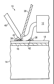
FIGURES 3A-B illustrate the soldering of electrical component 12 to
conductive track 16 of PCB 10, according to certain embodiments. As
illustrated in
FIGURE 3A, electrical component 12 may be soldered through coating 18 without
first removing coating 18 from conductive track 16. The soldering process may
comprise applying heat and solder 38 to a particular area of PCB 10 where
solder
joint 26 is to be formed. Heat may be applied to solder 38 using any suitable
heat
source such as, for example, a soldering iron 40. In some embodiments, the
soldering
process may also comprise applying flux 42 to the particular area of PCB 10.
The
heat, flux 42, and/or solder 38 may selectively alter coating 18 at the
particular area of
PCB 10. In some embodiments, altering coating 18 may refer to removing coating
18
from the particular area of PCB 10. Coating 18 may be removed by applying
solder
38, and optionally flux 42, to PCB 10 at a temperature and for a time such
that solder
38 bonds to conductive track 16 and coating 18 is locally dispersed, absorbed,
vaporised, dissolved, and/or degraded. In some embodiments, altering coating
18
may comprise changing the structure, porosity, and/or surface energy of
coating 18.
For example, fluxing may alter the surface energy of pores in coating 18,
which may
change the wettability of coating 18 such that solder 38 can flow through
pores in
coating 18 to conductive track 16. Thus, in this example, solder joint 26 may
form an
electrical connection through coating between electrical component 12 and
conductive track 16. As another example, the soldering process may selectively
alter
coating 18 by inducing voids (e.g., cracks) and/or causing voids to propagate
in the
particular area of coating 18 where solder 38 and/or flux 42 is applied.
Preferably,
one or more factors are configured so that the soldering process achieves good
solder
flow, covers a portion of conductive track 16 on substrate 14 with solder 38,
and/or
CA 02733765 2011-02-10
WO 2010/020753 PCT/GB2009/001966
27
forms a strong solder joint 26. These factors may include: (i) the
characteristics of
substrate 14, (ii) the characteristics of coating 18, (iii) the solder/flux
characteristics,
(iv) the soldering profile (including time and temperature), (v) the process
to disperse
coating 18, and (vi) the process to control solder flow around solder joint
26.
In some embodiments, the action of flux 42 and temperature alone may
interact with the halo-hydrocarbon polymers in coating 18 to alter coating 18
locally
at the particular area of PCB 10 to which flux 42 is applied. According to
certain
embodiments, altering coating 18 at the particular area of PCB 10 may comprise
removing coating 18 from the particular area of PCB 10. Solder 38 and/or flux
42
may be heated to any suitable temperature depending at least in part on the
composition of solder 38. In some embodiments, solder 38 and/or flux 42 are
heated
to between 200 C and 300 C. According to certain embodiments, solder 38
and/or
flux 42 are heated to between 240 C and 280 C. In a preferred embodiment
using
lead-free solder 38, solder 38 and/or flux 42 are heated to approximately 260
C.
The action of flux 42 and/or temperature may locally disperse, absorb,
vaporise, dissolve, and/or degrade coating 18 comprising halo-hydrocarbon
polymer.
Thus, coating 18 may only be altered at (e.g., removed from) the particular
area of
PCB 10 where solder 38 and/or flux 42 is applied. As illustrated in FIGURE 3B,
coating 18 may remain attached to the surface of PCB 10 right up until solder
joint
26. By abutting solder joint 26, coating 18 may provide environmental
protection of
conductive tracks 16 of PCB 10 right up to solder joint 26.
According to certain embodiments, there may be a balance between the time
required to alter coating 18, the temperature required to alter coating 18,
and/or the
acidity or aggressiveness of flux 42. Thus, milder fluxes 42 may suffice if
higher
temperatures are used, and vice versa. In some embodiments, a metal halide
layer
(e.g., copper fluoride) may reside between conductive track 16 and a halo-
hydrocarbon layer in coating 18. The metal halide layer may exhibit a self
fluxing
action when heat is applied to a particular area of PCB 10. The soldering
process may
take advantage of this self fluxing property. In some embodiments, the metal
halide
layer and/or the decomposition of halo-hydrocarbon polymers in coating 18 may
release fluorine and/or hydrogen fluoride (HF) to initiate fluxing (self
fluxing) during
CA 02733765 2011-02-10
WO 2010/020753 PCT/GB2009/001966
28
the soldering process. Due to this self fluxing property, if a sufficiently
high
temperature is used during the soldering process, solder joint 26 may be
formed
without using any flux 42.
Any suitable solder 38 may be used to form solder joint 26. In some
embodiments, solder 38 may be a fusible metal alloy having a melting point in
the
range of 90 C to 450 C. In some embodiments, solder 38 is a tin/lead solder
38
such as, for example, 60/40 Sn/Pb or 63/37 Sn/Pb. In other embodiments, solder
38 is
a lead-free solder 38 such as, for example, an alloy comprising tin, copper,
silver,
bismuth, indium, zinc, and/or antimony. Examples of lead-free solder 38
include
SnCuO.7, SnAg3.5Cu0.7, and SnAg3.0Cu0.5. In some embodiments, solder 38 may
comprise a powdered metal that is suspended in flux 42. The mixture of the
powdered metal and flux 42 may be referred to as a solder paste.
In embodiments using flux 42 to form solder joint 26, any suitable flux 42
may be used. In some embodiments, flux 42 may be a mild flux 42 such as, for
example, a "no-clean" flux (e.g., a rosin flux) that does not require a
subsequent step
of cleaning PCB 10. In other embodiments, flux 42 may be an organic flux 42
such
as, for example, an organic acid (e.g., lactic acid, acrylic acid, etc.), an
organic salt
(e.g., dimethylammonium chloride (DMA HCI)), and/or an organic amine (e.g.,
urea).
In yet other embodiments, flux 42 may be a resin/rosin flux 42 such as, for
example, a
synthetic resin or a natural rosin. In yet other embodiments, flux 42 may be
an
inorganic flux 42 such as, for example, an inorganic salt (e.g., zinc
chloride, sodium
chloride, potassium chloride, sodium fluoride, etc.) and/or an inorganic acid
(e.g.,
hydrochloric acid, nitric acid, etc.). In yet other embodiments, flux 42 may
be a
halide free flux, a no-residue flux, and/or a low solids flux. In addition, or
alternatively, industrial fluxes 42 may be used, such as, for example, fluxes
42 used
for general soldering, brazing, welding, cleaning, or etching a metal surface.
An
example of such an industrial flux 42 is borax. The choice of flux 42 may
depend on
the nature of coating 18, especially the particular thickness 24 and
composition of
coating 18. A thicker, more resistive coating 18 may require using a more
aggressive
flux 42. In addition, or alternatively, the choice of flux 42 may depend on
the wetting
properties of the materials in coating 18. A composition that comprises the
active
CA 02733765 2011-02-10
WO 2010/020753 PCT/GB2009/001966
29
ingredient or ingredients of flux 42 and that selectively alters coating 18 on
PCB 10
(e.g., selectively removes coating 18) may be used in place of flux 42.
As explained above, coating 18 permits the formation of good solder joints 26
on conductive tracks 16 of PCB 10. One or more factors may be controlled to
achieve
good quality, strong solder joints 26 on PCB 10. These factors may include:
(i) the
wetting characteristics and/or surface energy of the coated substrate 14
and/or PCB
10; (ii) the surface roughness of the coated substrate 14 and/or PCB 10; (iii)
the
surface roughness of conductive tracks 16 on substrate 14; (iv) the
composition of
solder 38 and/or solder paste (including active agents and/or solvents); (v)
the
temperature profile of the soldering process, which may include optimizing
profile
temperatures and residence times to improve wetting performance of solder 38,
solder
paste, and/or active components; (vi) the size and/or geometry of conductive
tracks 16
on the coated substrate 14; and/or (vii) the particle size of components
present in
solder 38 and/or solder paste. In some embodiments, the strength and/or
quality of
solder joint 26 may be enhanced by the pre-treatment, cleanliness, and/or
surface
preparation of conductive tracks 16 on substrate 14. Conductive tracks 16 may
be
cleaned by a surface treatment of plasma gas, sulphuric acid, and/or hydrogen
peroxide and/or by a persulphate-based etchant process. According to certain
embodiments, the aperture size and/or thicknesses of the solder paste stencil
may be
configured to control the quantity, position, wetting, and/or spread of the
solder paste
dispensed on conductive tracks 16 on the coated substrate 14.
In some embodiments, the quality and/or strength of solder joint 26 may be
enhanced by balancing the viscosity and surface tension of the solder paste
with
temperature to (i) control the wetting and flow of the solder paste on
conductive
tracks 16 and/or (ii) control the capillary action caused by electronic
components on
conductive tracks 16. This capillary action may tend to displace the solder
paste from
its desired location, especially if Fine Pitch and/or Ball Grid Array (BGA)
soldering is
used. According to certain embodiments, the quality and/or strength of solder
joint 26
may be enhanced by controlling the composition, chemical stability, and/or
thickness
24 of coating 18 such that the solder paste selectively alters coating 18 on a
particular
area on the surface of substrate 14. In some embodiments, the quality and/or
strength
CA 02733765 2011-02-10
WO 2010/020753 PCT/GB2009/001966
of solder joint 26 may be enhanced by controlling the chemical action of the
active
component in the solder paste with the halo-hydrocarbon polymers in coating 18
to
facilitate the selective alteration (e.g., selective removal) of coating 18.
The quantity
and/or composition of the active components in the solder paste may be
optimised to
5 facilitate this action.
Although FIGURES 3A-B illustrate a soldering process that uses solder 38,
heat, and flux 42 to form solder joint 26, it should be understood that solder
joint 26
may be formed through coating 18 using solder 38 and heat without any flux 42.
Although FIGURES 3A-B illustrate solder joint 26 formed through a single-layer
10 coating 18, it should be understood that solder joint 26 may be formed
through a
multi-layer coating 18.
FIGURE 4 illustrates PCB 10 comprising a multi-layer coating 18, according
to certain embodiments. The term "multi-layer" may refer to coating 18 that
comprises two or more distinct and/or graded layers 44 of polymers. Where a
multi-
15 layer coating 18 comprises distinct layers 44, each layer 44 may comprise a
discrete
chemical composition. Where a multi-layer coating 18 comprises graded layers
44,
individual layers 44 may form a region of intermediate composition between the
individual layers 44. The material(s) in the region of intermediate
composition may
have varying molecular weight, chemical composition, structure, geometry,
porosity,
20 and/or other properties. Thus, multi-layer coating 18 may comprise multiple
distinct
layers 44 of polymers and/or may comprise multiple graded layers 44 of
polymers.
In some embodiments, the multi-layer coating 18 may comprise a first layer
44a comprising a first type of polymer and a second layer 44b comprising a
second
type of polymer. In other embodiments, the first layer 44a and second layer
44b of
25 the multi-layer coating 18 may comprise polymers that have a similar
chemical
composition but different structures, different degrees of conjugation, and/or
different
weights. In some embodiments, a particular layer 44 in the multi-layer coating
18
may comprise a single type of halo-hydrocarbon polymer. In other embodiments,
a
particular layer 44 in the multi-layer coating 18 may comprise a mixture of
different
30 types of halo-hydrocarbon polymers. According to certain embodiments, each
layer
44 in the multi-layer coating 18 may comprise the same or different
compositions of
CA 02733765 2011-02-10
WO 2010/020753 PCT/GB2009/001966
31
polymer(s). In some embodiments, each layer 44 comprises similar precursor
compounds 36 that are processed differently to form each layer 44. This may
result in
each layer 44 having different polymers, different polymer networks, different
molecular weights, different sizes, different physical structures, and/or
differences in
other properties. In other embodiments, each layer 44 comprises different
precursor
compounds 36, which may cause each layer to comprise different materials
and/or
material properties.
The multi-layer coating 18 on PCB 10 may comprise any suitable number of
layers 44. In some embodiments, the multi-layer coating 18 comprises from two
to
five layers 44. In other embodiments, the multi-layer coating 18 comprises
from two
to four layers 44. In a preferred embodiment, the multi-layer coating 18
comprises
two or three layers 44. In embodiments where coating 18 comprises three or
more
layers 44, the multi-layer coating 18 may be configured such that two or more
layers
44 that are not adjacent to each other comprise the same polymer. For some
applications, the number of layers 44 in the multi-layer coating 18 may be
selected to
enhance the anti-reflective and/or dielectric properties of the multi-layer
coating 18.
In such embodiments, the multi-layer coating 18 may comprise a higher number
of
layers 44 (e.g., four or more) with the thickness and/or geometry of each
layer 44
being controlled. In such embodiments, a particular layer 44 in the multi-
layer
coating 18 may be chiral such that the particular layer 44 is ordered through
orientation and/or chemical structure.
A multi-layer coating 18 on PCB 10 may have any suitable thickness 24. For
example, a multi-layer coating 18 may have an overall thickness 24 from one nm
to
ten m, from one nm to five hundred nm, from three nm to five hundred nm, from
ten
nm to five hundred nm, from ten nm to two hundred and fifty nm, or from ten nm
to
thirty nm. In a preferred embodiment, a multi-layer coating 18 on PCB 10 has
an
overall thickness 24 from ten nm to one hundred nm, with one hundred nm being
a
preferred thickness 24.
The respective layers 44 within a multi-layer coating 18 may have any suitable
thickness. In some embodiments, the ratio of thicknesses of each layer 44 may
be
varied to achieve different properties of coating 18. In some embodiments,
each layer
CA 02733765 2011-02-10
WO 2010/020753 PCT/GB2009/001966
32
44 within coating 18 on PCB 10 may be of equal or approximately equal
thickness.
In other embodiments, one layer 44 may be thicker than other layer(s) 44 so
that a
multi-layer coating 18 exhibits overall properties that are tuned to provide
the
combined functionality derived from contributions from each layer 44 within
coating
18. According to certain embodiments, the thickness of a particular layer 44
may
comprise sixty to ninety percent of the overall thickness 24 of a multi-layer
coating
18, and the combined thickness of the remaining layer(s) 44 may comprise ten
to forty
percent of the overall thickness 24 of the multi-layer coating 18.
In embodiments where coating 18 comprises multiple graded layers 44, the
proportions of the respective polymers in the graded layers 44 may be varied
to
achieve different properties of the overall coating 18. Where coating 18
comprises
multiple graded layers 44, adjacent layers 44 may be fused together such that
polymers of intermediate chemical composition are present between adjacent
layers
44. In addition, or alternatively, a multi-layer coating 18 may comprise one
or more
polymer layers 44 adjacent to a layer 44 of metal halide (e.g., metal
fluoride).
According to certain embodiments, the proportion of each polymer in a graded,
multi-
layer coating 18 may be equal. In other embodiments of coating 18 comprising
graded layers 44 of different polymers, coating 18 may comprise more of a
particular
polymer than other polymer(s) such that the multi-layer coating 18 more highly
exhibits the properties of the particular polymer. In such embodiments, the
particular
polymer may make up sixty to ninety percent of coating 18 such that the
remaining
polymer(s) make up ten to forty percent of coating 18. As noted above, the
interface
between layers 44 may be well defined in some embodiments, and in other
embodiments, the interface between layers 44 may be graded.
According to certain embodiments, the first layer 44a of the multi-layer
coating 18 (i.e., the particular layer 44 abutting substrate 14 and/or
conductive tracks
16) is continuous or substantially continuous. In such embodiments, none or
substantially none of the second layer 44b may come into contact with
substrate 14
and/or conductive tracks 16 of PCB 10. One or more layers 44 of the multi-
layer
coating 18 may be deposited on substrate 14 and/or conductive tracks 16 prior
to the
soldering of any electrical components 12 to conductive tracks 16 on substrate
14.
CA 02733765 2011-02-10
WO 2010/020753 PCT/GB2009/001966
33
Accordingly, there may be no solder 38, or essentially no solder 38, between
one or
more layers 44 of the multi-layer coating 18 and conductive tracks 16.
As explained above, electrical components 12 may be connected to conductive
tracks 16 by various methods such as, for example, soldering and or wire
bonding. In
some embodiments, at least one layer 44 of a multi-layer coating 18 may be
optimized
for wire bonding and another layer of the multi-layer coating 18 may be
optimized for
soldering. For example, a first layer 44 that is optimized for wire bonding
may be
first deposited on conductive tracks 16. The wire bonding process may then be
executed to connect at least one electrical component 12 to conductive track
16. A
second layer 44 of the multi-layer coating 18 may then be deposited over PCB
10.
The second layer 44 may be optimized for soldering. Another electrical
component
12 may then be soldered through the multi-layer coating 18 to conductive track
16.
Alternatively, the foregoing steps could be reversed such that the particular
layer 44
that is optimized for soldering could be deposited, then the soldering could
be
performed, then the particular layer 44 that is optimized for wire bonding
could be
deposited, and then the wire bonding could be performed.
In some embodiments, coating 18 comprises at least one layer 44 comprising a
low-halogen-containing hydrocarbon polymer. A low-halogen-containing
hydrocarbon polymer may be any suitable polymer having less than a threshold
quantity of halogen atoms. For example, a low-halogen-containing hydrocarbon
polymer may refer to a polymer having less than a configurable percentage (by
mass)
of halogen atoms (e.g., less than two percent by mass, less than 0.5 percent
by mass,
and/or any suitable percentage).
According to certain embodiments, coating 18 comprises at least one layer 44
comprising a halo-hydrocarbon polymer and another layer 44 comprising a non-
halo-
hydrocarbon polymer. In some embodiments, a non-halo-hydrocarbon polymer may
be any suitable polymer that does not comprise halogen atoms. A non-halo-
hydrocarbon polymer may have a straight or branched chain or ring carbon
structure.
In some embodiments, there may be crosslinking between the chains of a non-
halo-
hydrocarbon polymer. A non-halo-hydrocarbon polymer may comprise one or more
unsaturated groups such as, for example, carbon-carbon double and/or triple
bonds.
CA 02733765 2011-02-10
WO 2010/020753 PCT/GB2009/001966
34
In some embodiments, a non-halo-hydrocarbon polymer comprises one or more
heteroatoms (i.e., atoms that are not carbon, hydrogen, or a halogen) such as,
for
example, nitrogen, sulphur, silicon, and/or oxygen. According to certain
embodiments, the molecular weight of a non-halo-hydrocarbon polymer is greater
than five hundred amu. A non-halo-hydrocarbon polymer may be a polymer that
can
be deposited by plasma deposition.
A particular layer 44 of coating 18 may comprise any suitable non-halo-
hydrocarbon polymer(s). For example, the particular layer 44 may comprise a
polyalkene, a polyester, a vinyl polymer, a phenolic resin, and/or a
polyanhydride. In
a preferred embodiment, the particular layer 44 comprises a polyalkene such
as, for
example, polythene and/or polypropylene.
In some embodiments, PCB 10 may comprise coating 18 comprising (i) a first
layer 44a of a non-halo-hydrocarbon polymer that is deposited directly on
substrate 14
and/or conductive tracks 16 and (ii) a second layer 44b of a halo-hydrocarbon
polymer that is deposited on the first layer 44a. Such embodiments may be
advantageous where a metal halide layer 44 on conductive tracks 16 is not
desirable.
In particular, depositing a first layer 44a of a non-halo-hydrocarbon polymer
directly
on conductive tracks 16 may prevent the formation of a metal halide layer 44
on
conductive tracks 16. In some embodiments, a metal halide layer 44 may be
undesirable if it results, for example, in intermetallics that are vulnerable
to
weakening under specific environmental conditions. In such embodiments, a
first
layer 44a comprising a non-halo-hydrocarbon polymer may serve as a barrier
between
conductive tracks 16 and a second layer 44b comprising a halo-hydrocarbon
polymer.
Thus, the formation of a first layer 44a comprising a non-halo-hydrocarbon
polymer
may prevent the formation of a metal halide layer 44 during subsequent
deposition of
a layer 44 comprising a halo-hydrocarbon polymer.
In other embodiments, a metal halide layer may be desired. In such
embodiments, coating 18 may comprise (i) a first layer 44a of a metal halide
that is
formed directly on substrate 14 and/or conductive tracks 16 and (ii) a second
layer
44b of a halo-hydrocarbon polymer that is deposited on the first layer 44a.
CA 02733765 2011-02-10
WO 2010/020753 PCT/GB2009/001966
Although one or more embodiment described above comprise a first layer 44a
of a non-halo-hydrocarbon polymer and a second layer 44b of a halo-hydrocarbon
polymer, it should be understood that, in other embodiments, all, some, or
none of the
layers 44 of a multi-layer coating 18 may comprise a halo-hydrocarbon polymer.
It
5 should be further understood that all, some, or none of the layers 44 of the
multi-layer
coating 18 may comprise a non-halo-hydrocarbon polymer.
A multi-layer coating 18 on PCB 10 may be configured to offer varying and/or
customized performance. In some embodiments, layers 44 of a multi-layer
coating 18
may be configured to optimize the conductivity, oxidation resistance,
environmental
10 protection, cost, moisture absorption/resistance, dendrite prevention,
flame
retardancy, and/or other optical, electrical, physical, and/or chemical
properties of the
multi-layer coating 18. For example, a relatively thick coating 18 that is
highly
fluorinated may be desirable to provide good environmental protection in
certain
embodiments, while in other embodiments, a relatively thin coating 18
comprising
15 less halide may be preferred. As described above with respect to FIGURES 3A-
B,
electrical components 12 may be soldered through a multi-layer coating 18 to
conductive tracks 16 without first removing the multi-layer coating 18.
According to certain embodiments, a multi-layer coating 18 on PCB 10
comprises a first layer 44a comprising a first type of halo-hydrocarbon
polymer and a
20 second layer 44b comprising a second type of halo-hydrocarbon polymer. In
some
embodiments, a multi-layer coating 18 comprises a particular layer 44 of a
polytetrafluoroethylene (PTFE) type material and another layer 44 of a
polychlorotrifluoroethylene (PCTFE) type material. The PCTFE layer 44 may be
deposited directly on substrate 14 and/or conductive tracks 16 and the PTFE
layer 44
25 may be deposited on the PCTFE layer 44. In such embodiments, the PCTFE
layer 44
may prevent oxidation of conductive tracks 16 and the PTFE layer 44 may
provide
environmental protection for PCB 10. In other embodiments, the PTFE layer 44
may
be deposited directly on substrate 14 and/or conductive tracks 16 and the
PCTFE
layer 44 may be deposited on the PTFE layer 44. This may allow the external
30 physical and/or chemical properties of the surface of PCB 10 to be
determined by the
PCTFE layer 44.
CA 02733765 2011-02-10
WO 2010/020753 PCT/GB2009/001966
36
Although FIGURE 4 illustrates a multi-layer coating 18 having distinct layers,
it should be understood that the multi-layer coating 18 may have graded
layers.
Although a PTFE layer 44 and a PCTFE layer 44 of a multi-layer coating 18 are
described above, it should be understood that the multi-layer coating 18 may
comprise
any suitable types and/or combinations of materials. In some embodiments, the
material(s) in the multi-layer coating 18 may not be PTFE type and/or PCTFE
type
materials.
FIGURE 5 illustrates PCB 10 comprising a multi-layer coating 18 selectively
applied to particular regions of PCB 10, according to certain embodiments. As
illustrated, particular regions of PCB 10 may be coating 18 with a single-
layer coating
18 and other regions of PCB 10 may be coated with a multi-layer coating 18.
Thus,
different regions of PCB 10 may be coated with different polymers, or mixtures
thereof, to achieve different properties in the different regions. For
example, in a first
region of PCB 10 it may be desirable to have a multi-layer coating 18 that
exhibits
piezo-electric and/or electroresistive properties, while in a second region of
PCB 10 it
may be desirable to have a single-layer coating 18 that exhibits electrically
insulating
properties. In this example, one may apply to the first region of PCB 10 a
multi-layer
coating 18 having a first layer 44a comprising a polymer of vinylidenefluoride
(PVDF) and a second layer 44b comprising another halo-hydrocarbon polymer.
Layer 44 of PVDF may enhance the piezo-electric, electroresistive, and/or
electrostrictive properties of coating 18 in the first region of PCB 10. In
this example,
one may apply to the second region of PCB 10 a single-layer coating 18
comprising a
halo-hydrocarbon polymer or a non-halo-hydrocarbon polymer that exhibits
greater
insulation properties that PVDF. Thus, particular regions of PCB 10 may be
coated
with a single-layer coating 18 and other regions of PCB 10 may be coated with
a
multi-layer coating 18.
Although the foregoing example illustrates coating 18 comprising PVDF, it
should be understood that any suitable polymers may be used in any single-
layer
and/or multi-layer coating 18.
A multi-layer coating 18 may be applied to PCB 10 using any suitable
technique. For example, a multi-layer coating 18 may be deposited using plasma
CA 02733765 2011-02-10
WO 2010/020753 PCT/GB2009/001966
37
deposition, chemical vapour deposition (CVD), molecular beam epitaxy (MBE),
plasma enhanced-chemical vapour deposition (PE-CVD), high pressure/atmospheric
plasma deposition, metallo-organic-chemical vapour deposition (MO-CVD), and/or
laser enhanced-chemical vapour deposition (LE-CVD). In some embodiments, a
multi-layer coating 18 may be deposited by the creation of inter-penetrating
polymer
networks (IPNs) and/or by surface absorption of monolayers (SAMs) of polymers
or
monomers to form in-situ polymers and/or polymer alloys. In other embodiments,
a
multi-layer coating 18 may be deposited using a liquid coating technique such
as, for
example, liquid dipping, spray coating, spin coating, sputtering, and/or a sol-
gel
process. In embodiments comprising multi-layer coatings 18, each layer 44 may
be
formed using the same or different techniques.
In some embodiments, a multi-layer coating 18 is applied to PCB 10 using the
plasma deposition technique described above with respect to FIGURE 2. In such
embodiments, once conductive tracks 16 are formed on substrate 14, substrate
14 may
be placed in chamber 30 in reactor 28. Reactor 28 may introduce gases (e.g.,
hydrogen, argon, and/or nitrogen) into chamber 30 to clean substrate 14.
Reactor 28
may then introduce one or more precursor compounds 36 into chamber 30 to form
a
multi-layer coating 18 on substrate 14 by plasma deposition. In some
embodiments,
the multi-layer coating 18 may follow the three dimensional form of substrate
14
and/or conductive tracks 16 of PCB 10.
A multi-layer coating 18 (comprising either distinct or graded layers 44) may
be deposited on substrate 14 by varying the composition of precursor compounds
36
introduced into chamber 30. In some embodiments, one or more precursor
compounds 36 may be used to generate a gas mixture in chamber 30. The mixture
of
precursor compounds 36 may be configured to generate graded layers 44 of
coating
18 on substrate 14. In other embodiments, distinct layers 44 of coating 18 may
be
deposited on substrate 14 by switching between precursor compounds 36 and
modifying conditions in chamber 30. The composition of a multi-layer coating
18
may be controlled by one or more of the following factors: (i) the plasma gas
selected;
(ii) the particular precursor compound(s) 36 used; (iii) the amount of
precursor
compound(s) 36 (which may be determined by the combination of the pressure of
CA 02733765 2011-02-10
WO 2010/020753 PCT/GB2009/001966
38
precursor compound(s) 36 and flow rate); (iv) the ratio of precursor
compound(s) 36;
(v) the sequence of precursor compound(s) 36; (vi) the plasma pressure; (vii)
the
plasma drive frequency; (viii) the pulse width timing; (ix) the coating time;
(x) the
plasma power (including the peak and/or average plasma power); (xi) the
chamber
electrode arrangement; (xii) the preparation of the incoming PCB 10; and/or
(xiii) the
size and geometry of chamber 30. Coating 18 deposited by plasma deposition may
completely, or substantially completely, encapsulate all surfaces of PCB 10.
As a
result, coating 18 may stop or reduce aqueous absorption and "wetting" of PCB
10.
This may significantly reduce any corrosive action from within substrate 14
and/or
from under or adjacent to conductive tracks 16. This may be especially
advantageous
for epoxy-based PCBs 10 and paper/card PCBs 10, which may tend to absorb
water,
aqueous acids, and/or corrosive materials and which may be vulnerable to
corrosion
by such in-situ mechanisms.
Plasma deposition may be used to deposit layer(s) 44 of halo-hydrocarbon
polymers and/or layer(s) 44 of non-halo-hydrocarbon polymers. Precursor
compounds 36 for halo-hydrocarbon polymers are described above with respect to
FIGURE 2. With respect to non-halo-hydrocarbon polymers, precursor compounds
36 may be hydrocarbon materials that are selected to provide the desired
coating 18
properties. When introduced into the gas plasma, the particular precursor
compounds
36 may be ionized/decomposed to generate a range of active species that will
react at
the surface of PCB 10 (e.g., by a polymerisation process) to generate a thin
layer 44
of a non-halo-hydrocarbon polymer. Any suitable precursor compounds 36 may be
used to form a non-halo-hydrocarbon layer 44. Examples of precursor compounds
36
for depositing layer 44 of a non-halo-hydrocarbon polymer are alkanes,
alkenes, and
alkynes.
As explained above, PCB 10 may be coated with complex, three-dimensional
coatings 18. Such coatings 18 may comprise a single layer 44 over particular
regions
of PCB 10 and multiple layers 44 over other regions of PCB 10. Any suitable
techniques may be used to form such coatings 18. In some embodiments, one or
more
layers 44 of coating 18 may be deposited only on selective areas of PCB 10.
For
example, one or more layers 44 of coating 18 may be selectively deposited (i)
by
CA 02733765 2011-02-10
WO 2010/020753 PCT/GB2009/001966
39
masking the surface of PCB 10 to deposit coating 18 only in non-masked areas,
(ii) by
using photo-assisted plasma deposition techniques (e.g., laser or UV light
assisted),
and/or (iii) by using metallo-organic chemical vapour deposition (MOCVD) type
precursor compounds 36 such as, for example, metal-alkyl and/or carbonyl
precursors. In other embodiments, coatings 18 may be formed using one or more
subtractive techniques.
According to certain embodiments, the deposition process may be configured
to modify the wetting characteristics of coating 18 on PCB 10. Wetting may
refer to
(i) the wetting of the surface of the coated PCB 10 by liquids such as water,
(ii) the
wetting of coating 18 by solder 38 and/or flux 42 during the soldering
process, and/or
(iii) the wetting of conductive tracks 16 by solder 38 after coating 18 has
been altered
(e.g., locally removed). The wetting characteristics of coating 18 may be
modified
according to any suitable technique. For example, the wetting characteristics
of
coating 18 may be modified by plasma etching using reactive gas plasmas such
as, for
example, carbon tetrafluoride (CF4). As another example, the wetting
characteristics
of coating 18 may be modified by plasma activation using gas plasmas selected
to
provide the desired surface activation such as, for example, gas plasmas based
on
hydrogen, oxygen, argon, nitrogen, and/or combinations of such gases. As yet
another example, the wetting characteristics of coating 18 may be modified by
plasma
polymerisation and/or by using variants of and/or mixtures of halo-
hydrocarbons
(e.g., fluoro-hydrocarbons, chloro-hydrocarbons, etc.) and/or non-halo-
hydrocarbons
(e.g., polyethylene, polypropylene, etc.). As yet another example, the wetting
characteristics of coating 18 may be modified by liquid based chemical
etching,
which may modify the surface activation and/or surface roughness of coating 18
using, for example, strong acids (e.g., sulphuric acid, nitric acid, etc.)
and/or oxidizing
agents (e.g., hydrogen peroxide). In some embodiments, the wetting
characteristics of
coating 18 may be spatially controlled to provide different regions of PCB 10
having
different wetting characteristics. A region (on the surface of PCB 10) that
has
enhanced wetting characteristics may selectively control the direction in
which liquid
flows across PCB 10. Thus, such a region may act as a "gutter" to direct
liquid run-
off to areas where the liquid will not cause damage.
CA 02733765 2011-02-10
WO 2010/020753 PCT/GB2009/001966
In some embodiments, some or all surfaces of PCB 10 may be completely or
substantially encapsulated with coating 18. This may protect PCB 10 and/or
prevent
aqueous absorption and/or "wetting" of PCB 10. In addition, or alternatively,
this
may reduce any corrosive action from within substrate 14 or from under or
adjacent to
5 conductive tracks 16. Thus, coating 18 may protect PCB 10 having an epoxy-
based,
paper-based, and/or card based substrate 14 which would otherwise absorb
liquids
(e.g., water, aqueous acids, and corrosive materials) and which may otherwise
be
vulnerable to corrosion.
PCB 10 comprising coating 18 may provide advantages over uncoated PCBs
10 10. The disclosed coating 18 may provide none, some, or all of the
following
advantages. One advantage is that, in some embodiments, coating 18 may permit
PCB 10 to operate in harsh and/or corrosive environments. Traditional PCBs 10
have
generally been unable to reliably function in such environments. Conductive
tracks
16 on uncoated PCBs 10 may corrode, which may result in a far shorter lifetime
of the
15 device than would normally be expected. This may occur, for example, when
an
uncoated PCB 10 is used in very humid environments, especially where
microscopic
droplets of water comprising dissolved gases such as sulphur dioxide, hydrogen
sulphide, nitrogen dioxide, hydrogen chloride, chlorine, ozone, and/or water
vapour
form a corrosive solution. This may lead to a thin film or corrosion deposit
forming
20 between conductive tracks 16 on the uncoated PCB 10, which may cause short
circuits. In some cases, manufacturers have applied conformal coatings of a
polymer
to PCB 10 after soldering electrical components 12 to PCB 10. However, such
conformal coatings are generally expensive. Applying such conformal coatings
may
require an extra step in the manufacturing process after electrical components
12 have
25 been soldered to PCB 10. Such conformal coatings may also require another
step to
remove the conformal coating when it is necessary to rework a damaged or
failed
PCB 10 or when it is necessary to test PCB 10 to ascertain its performance or
troubleshoot a problem. In contrast to such conformal coatings, coating 18
comprising a halo-hydrocarbon polymer may represent a lower cost and/or higher
30 performance solution for protecting PCB 10 in harsh and/or corrosive
environments.
In some embodiments, one or more layers 44 of coating 18 may be applied in a
CA 02733765 2011-02-10
WO 2010/020753 PCT/GB2009/001966
41
conformal fashion to PCB 10 after attaching (e.g., soldering, wire bonding,
etc.)
electrical components 12 to conductive tracks 16. Thus, coating 18 may be
applied to
a populated PCB 10 as a conformal coating 18 that provides one or more
advantages
described herein (e.g., oxidation/corrosion resistance, solder-through
capability, wire
bonding capability, z-axis conductivity, etc.).
Another advantage is that, in some embodiments, coating 18 may prevent
substrate 14, conductive tracks 16, and/or other elements of PCB 10 from
absorbing
water and/or solvents. The elements of traditional PCBs 10 may comprise
materials
that absorb water and/or solvents (including aqueous, organic, inorganic,
and/or
mixed solvents) in liquid, vapour, and/or gaseous form. For example,
substrates 14
comprising fabrics (e.g., epoxy resin bonded glass fabrics), paper (e.g.,
synthetic resin
bonded paper, cotton paper, phenolic cotton paper, epoxy, paper, cardboard,
etc.),
textiles, and/or wood based materials (natural and/or synthetic) may absorb
water
and/or solvent-based chemicals. As another example, conductive tracks 16
comprising metals, conductive polymers, and/or printed conductive inks may
absorb
water and/or solvent-based chemicals. As yet another example, PCB 10 may
comprise magnetic structures, printed magnetic inks, and/or other elements
that may
absorb water and/or solvent-based chemicals. Thus, PCB 10 may comprise porous
and/or hydrophilic structures having a natural tendency for water and/or
solvents that
may cause changes to those structures. (The tendency of a material to interact
with
water and/or solvents in the liquid phase or through condensation from the gas
phase
may include solid solvents.) When elements of PCB 10 absorb water and/or
solvents,
one or more problems may result. These problems may include: (i) increased
mechanical stresses during thermal cycles due to differences in thermal
expansion
coefficients; (ii) alteration of adhesion properties of PCB elements; (iii)
alterations to
the dielectric constant and loss tangent of PCB elements; (iv) swelling of the
structure
rendering some materials unsuitable for plated through holes and/or for use in
some
high humidity conditions, especially where high voltages are used; (v)
corrosion of
conductive tracks 16 at or around the interface between conductive tracks 16
and
substrate 14; (vi) loss of mechanical strength; (vii) reordering of material
in PCB 10
CA 02733765 2011-02-10
WO 2010/020753 PCT/GB2009/001966
42
in the presence of water; and/or (viii) electrolysis in the presence of an
applied field
leading to corrosion and/or degradation of PCB 10.
Another advantage may be realized where conductive tracks 16 comprise a
conductive ink polymer. Conductive ink polymers may tend to absorb liquids
and/or
moisture, which may result in swelling, modification of electrical properties,
and/or
degradation of circuit performance. In addition, or alternatively, printed
active
devices (e.g., as used in plastic electronics) may absorb water and/or solvent-
based
chemicals, which may change the performance and/or properties of printed
active
devices. Applying coating 18 to printed active devices and/or conductive
tracks 16
comprising conductive ink polymers may prevent water absorption.
In some embodiments, coating 18 may be configured to exhibit conductivity
along an axis pointing into the plane of the coated surface (the "z-axis" 22)
while
acting as an insulator along the axes parallel to the coated surface (the "x-
axis" 46 and
the "y-axis" 48). Accordingly, coating 18 may be applied to a conductive
contact 50
without hindering the ability of such contact 50 to transmit an electrical
signal and/or
carry current to a mating contact 50. Thus, in some embodiments, coating 18
may
protect contacts 50 from oxidation and/or corrosion without hindering the
conductivity of contacts 50.
FIGURES 6A-B illustrate a keypad 52 comprising contacts 50 that are coated
with coating 18, according to certain embodiments. Keypad 52 may be an input
device comprising a plurality of keys 54. By depressing key 54, user may cause
keypad 52 to transmit an electrical signal. Keypad 52 may be any suitable type
of
input device that comprises keys 54. For example, keypad 52 may be a dome-
switch
keypad 52, a membrane keypad 52, and/or any suitable keypad 52.
Keypad 52 may comprise a plurality of keys 54. In some embodiments, each
key 54 comprises an exposed surface 56 that is visible to a user and a
concealed
surface 58 that is generally not visible to the user. A conductive contact 50
may be
attached to the concealed surface 58 of each key 54 in keypad 52. In some
embodiments, keypad 52 comprises PCB 10 having a plurality of conductive
contacts
50. Each contact 50 on PCB 10 may correspond to one or more keys 54 of keypad
52.
Thus, when a user depresses a particular key 54, contact 50 attached to key 54
may
CA 02733765 2011-02-10
WO 2010/020753 PCT/GB2009/001966
43
touch the corresponding contact 50 attached to PCB 10, thus allowing an
electrical
signal to flow (e.g., by closing an open circuit).
Keypad 52 may comprise any suitable type of keys 54. Examples of keys 54
include metal "snap dome" keys 54, spring actuated keys 54, and silicon rubber
buttons having one or more carbon inserts. In some embodiments, key 54 may
represent an area of a membrane keypad 52. A membrane keypad 52 may comprise
two membrane layers (e.g., plastic or polymer substrates) that are normally
separated
by an air space. The inner surfaces of the two membranes may comprise flexible
contacts 50 such as, for example, conductive inks (e.g., silver ink),
conductive glues,
and/or conductive adhesives. The depression of key 54 of a membrane keypad 52
may cause contacts 50 of the two membranes to touch, resulting in transmission
of a
signal. It should be understood that keypad 52 may comprise any suitable type
and/or
combination of keys 54.
Contact 50 in keypad 52 may be any suitable conductive device for joining
and/or closing an electrical circuit. Contact 50 may comprise an electrode,
connector,
pin, pad, and/or any suitable conductive device. Contact 50 may comprise any
suitable conductive material. For example, contacts 50 may comprise one or
more
metals such as, for example, stainless steel, nickel, tin, copper, aluminium,
gold,
silver, and/or any suitable alloy thereof. In some embodiments, contacts 50
may
comprise conductive inks, silver loaded epoxy, conductive plastics, and/or non-
metallic conductive materials such as, for example, carbon and/or graphite.
Thus,
contacts 50 may comprise any suitable type and/or combination of conductive
materials.
In some embodiments, one or more contacts 50 in keypad 52 may be coated
with coating 18. As explained above, coating 18 may be configured to be
electrically
conductive in the z-axis direction but to act as an insulator in the x-axis
and y-axis
directions. In other words, coating 18 may exhibit higher impedance and/or
resistance
in the x-axis and y-axis directions but low impedance and/or resistance in the
z-axis
direction. This property may allow contact 50 coated with coating 18 to
conduct an
electrical signal and/or current through coating 18 to a mating contact 50.
CA 02733765 2011-02-10
WO 2010/020753 PCT/GB2009/001966
44
Coating 18 on contact 50 in keypad 52 may have any suitable thickness 24. In
some embodiments, thickness 24 of coating 18 on contact 50 is from one nm to
two
gm. In other embodiments, thickness 24 of coating 18 may be from one nm to
five
hundred nm. In yet other embodiments, thickness 24 of coating 18 may be from
three
nm to five hundred nm. In yet other embodiments, thickness 24 of coating 18
may be
from ten nm to five hundred nm. In yet other embodiments, thickness 24 of
coating
18 may be from ten nm to two hundred and fifty nm. In yet other embodiments,
thickness 24 of coating 18 may be from ten nm to thirty nm. In yet other
embodiments, coating 18 is a monolayer of a halo-hydrocarbon polymer (having
thickness 24 of a few angstroms (A)). In a preferred embodiment, thickness 24
of
coating 18 is from ten nm to one hundred nm in various gradients, with one
hundred
nm being a preferred thickness 24.
In some embodiments, the optimal thickness 24 of coating 18 may depend on
the coating properties that are desired. For example, if very high
environmental
toughness is required (e.g., high corrosion and abrasion resistance), a
thicker coating
18 may be preferred. In some embodiments, thickness 24 of coating 18 may be
optimised with different thicknesses 24 at different locations of the device,
depending
on which properties are being optimised (e.g., environmental protection versus
z-axis
conductivity). Coating 18 may be optimised for compliance to avoid cracking
when
flexed; to minimise wear on coating 18 and/or wear caused by coating 18; for
environmental protection; for physical protection of a softer, underlying
material; for
controlled resistance for circuit trimming; for stability for reference
measurements of
sensors/electrodes; and/or for surface energy, charge dissipation, and/or
blooming.
As noted above, contact 50 coated with coating 18 may conduct an electrical
signal and/or current through coating 18 to a mating contact 50. In this
context, the
phrase "conduct through" may refer to conducting an electrical signal and/or
current
between two or more contacts 50 without removing coating 18. Thus, coating 18
may
be deposited between at least two mating contacts 50 and then a signal and/or
current
may be conducted between the mating contacts 50 without removing coating 18.
The
ability to conduct a signal and/or current through coating 18 may be due at
least in
part to the low impedance and/or resistance of coating 18 in the z-axis
direction.
CA 02733765 2011-02-10
WO 2010/020753 PCT/GB2009/001966
Thus, the phrase "conduct through" may refer to conducting an electrical
signal
and/or current between two or more contacts 50 without removing coating 18.
The conductivity of coating 18 may be measured according to any suitable
technique. In some embodiments, the conductivity of coating 18 may be measured
by
5 determining the resistance of coating 18. Such measurement may be achieved
by
soldering conductive wires to contacts 50 and connecting wires to a resistance
meter
60. A predetermined force 62 may cause contacts 50 to touch each other (e.g.,
be
brought into electrical contact). As illustrated in FIGURE 6B, resistance
meter 60
may then measure the resistance through coating 18 between the corresponding
10 contacts 50. As a reference point, the resistance of contacts 50 themselves
may be
determined by measuring the resistance between uncoated contacts 50. According
to
certain embodiments, coating 18 may exhibit z-axis resistance in a range from
zero to
ten kilo-ohms (kf ). In a preferred embodiment, coating 18 may exhibit z-axis
resistance in a range from zero to one ohms (a).
15 FIGURE 7 is a graph 64 illustrating the z-axis resistance of example
coatings
18 having various thicknesses 24, according to certain embodiments. The
metrics
illustrated in graph 64 are example values of z-axis resistance for example
coatings
18. It should be understood, however, that coatings associated with different
materials, structures, deposition techniques, and/or other factors may exhibit
different
20 amounts of z-axis conductivity. Although graph 64 illustrates z-axis
resistance in
relation to thickness 24, it should be understood that other variables (e.g.,
materials,
structure, deposition method, etc.) may affect the z-axis conductivity of
coating 18.
In the illustrated example, the z-axis resistance of an example coating 18 on
keypad 52 was measured using resistance meter 60, as illustrated in FIGURE 6B.
25 Contacts 50 in this example were coated with a PTFE type material. A metal
"snap-
dome" key 54 was used as one of contacts 50. Electrical wires were soldered to
contacts 50 and connected to resistance meter 60. A predetermined force 62
(approximately five Newton meters) was applied to one contact 50, causing that
contact 50 to touch a corresponding contact 50. Resistance meter 60 then
measured
30 the electrical resistance between the touching contacts 50. The
predetermined force
62 was applied by using ENIG plated tracks and by varying force 62 until a
stable
CA 02733765 2011-02-10
WO 2010/020753 PCT/GB2009/001966
46
resistance measurement was made. The measurement was repeated for coatings 18
of
different thicknesses 24. The resulting readings were adjusted to account for
(i) the
fact that two thicknesses 24 of coating 18 (i.e., one thickness 24 for each
contact 50)
were present in the measurement path and (ii) the resistance of the particular
contacts
50 without coating 18. The resistance of contacts 50 was determined by using
an
uncoated PCB 10 as a reference.
The results of these measurements are illustrated in graph 64 in FIGURE 7
and in the table below. Graph 64 in FIGURE 7 comprises a first axis 66 that
corresponds to the resistance of coating 18 and a second axis 68 that
corresponds to
thickness 24 of coating 18. The measured resistances are illustrated as points
70 in
graph 64.
Coating thickness Resistance of coating
(nm) f
30 0.0704
40 0.1677
50 0.2095
75 0.4105
200 1.2775
Although the foregoing example illustrates the resistance of a particular
coating 18 comprising a PTFE type material, it should be understood that
coating 18
may comprise any suitable type and/or combination of halo-hydrocarbon
polymers.
Although the foregoing example illustrates the resistance of coating 18 having
particular thicknesses 24, it should be understood that coating 18 may be
configured
to have any suitable thickness 24.
Generally, contacts 50 in a device may be coated with coating 18 before or
after construction of the device. In a preferred embodiment, contacts 50 are
coated
with coating 18 before construction of the device. Coating 18 may be applied
to one,
some, or all of the surfaces of contact 50. In some embodiments, coating 18
may be
applied to one or more surfaces of the device (e.g., keypad 52). Coating 18
may be
applied to surfaces of contact 50 and/or device that will be exposed to the
environment such as, for example, surfaces that act as electrical contact
areas between
two or more parts of a circuit. Applying coating 18 to the surfaces of device
in
CA 02733765 2011-02-10
WO 2010/020753 PCT/GB2009/001966
47
addition to the surfaces of contact 50 may (i) increase the protection of the
device
from corrosion and/or oxidation and/or (ii) prevent the formation of spoilage
routes to
contact areas in device.
Coating 18 may be deposited on contacts 50 according to any suitable
technique. For example, coating 18 may be deposited using chemical vapour
deposition (CVD), molecular beam epitaxy (MBE), plasma enhanced-chemical
vapour deposition (PE-CVD), high pressure/atmospheric plasma deposition,
metallo-
organic-chemical vapour deposition (MO-CVD), and/or laser enhanced-chemical
vapour deposition (LE-CVD). In some embodiments, coating 18 may be deposited
on
contacts 50 by the creation of inter-penetrating polymer networks (IPNs)
and/or by
surface absorption of monolayers (SAMs) of polymers or monomers to form in-
situ
polymers and/or polymer alloys. In other embodiments, coating 18 may be
deposited
using a liquid coating technique such as, for example, liquid dipping, spray
coating,
spin coating, sputtering, and/or a sol-gel process.
According to certain embodiments, coating 18 may be deposited on contacts
50 using plasma deposition, as described above with respect to FIGURE 2. Thus,
contacts 50 may be placed in chamber 30 in reactor 28. Reactor 28 may then
introduce gases (e.g., hydrogen, argon, and/or nitrogen) into chamber 30 to
clean
contacts 50. In one or more steps, reactor 28 may then introduce one or more
precursor compounds 36 into chamber 30 to form a single-layer or multi-layer
coating
18 on contacts 50 by plasma deposition. In some embodiments, coating 18 may
follow the three dimensional form of contact 50. The preferred method for
depositing
coating 18 on contacts 50 may depend on the particular thickness 24 of coating
18
that is desired. Liquid coating techniques may be preferred for thicker
coatings 18,
while plasma deposition may be preferred for thinner coatings 18.
The technique used to deposit coating 18 on contacts 50 may be configured to
control the z-axis conductivity of coating 18. In some embodiments, the z-axis
conductivity of coating 18 may be controlled by regulating one or more of the
following factors:
CA 02733765 2011-02-10
WO 2010/020753 PCT/GB2009/001966
48
^ Composition of halo-hydrocarbon material in coating 18, which may
include combining different halo-hydrocarbon materials and controlling
the gradation between layers 44 of the different materials.
^ Ratios of halogen atoms/hetero-atoms/carbon atoms in the halo-
hydrocarbon material in coating 18.
^ Proportion of carbon in the halo-hydrocarbon coating material.
^ Degree of conjugation in the halo-hydrocarbon coating material.
^ Average molecular weight of the halo-hydrocarbon coating material.
^ Degree of branching and cross-linking in the halo-hydrocarbon coating
material.
^ Molecular size distribution of molecules in the halo-hydrocarbon coating
material.
^ Density of the halo-hydrocarbon coating material.
^ Presence of additional doping agents in the halo-hydrocarbon coating
material.
^ Presence of ionic/salt, ionic, and/or covalent components in the halo-
hydrocarbon coating material.
^ Presence of organic/polymer and inorganic compounds comprising
transition metals, including complex cations and anions in the halo-
hydrocarbon coating material.
^ Presence of compounds and/or elements having variable oxidation states in
the halo-hydrocarbon coating material.
^ Presence of chemical compounds having delocalized character in the halo-
hydrocarbon coating material.
^ Presence of occluded components in the halo-hydrocarbon coating
material.
^ When coating 18 is deposited by plasma deposition, adjustment of plasma
conditions (e.g. power, gas pressure, electrode arrangement).
^ Thickness of the halo-hydrocarbon coating material (e.g., thicker coatings
18 may exhibit greater resistance than thinner coatings 18 of the same
material).
CA 02733765 2011-02-10
WO 2010/020753 PCT/GB2009/001966
49
^ Orientation of coating 18.
^ Continuity of coating 18 (e.g., porosity and/or three-dimensional
structure).
Although keypad 52 is described in the examples above, coating 18 may be
applied to contacts 50 in any type of device. For example, coating 18 may be
applied
to contacts 50 in safety switches, alarm switches, fuse holders, keypads 52 on
mobile
telephones, touch screens, batteries, battery terminals, semiconductor chips,
smart
cards, sensors, test chips, elastomeric connectors (e.g., Zebra strips),
electrical
connectors (e.g., sockets and plugs), terminators, crimped connectors, press-
fit
connectors, and/or sliding contacts 50 such as, for example, those used in
chips, smart
cards, tokens, and/or reader mechanisms.
FIGURE 8 illustrates a measuring device 72 comprising a sensor 74 having
coated contacts 50, according to certain embodiments. Sensor 74 may be any
suitable
type of sensor 74. In some embodiments, sensor 74 is a disposable sensor 74
that
measures analytes such as, for example, toxic gases, glucose, physiological
fluid-
based chemical compounds, and/or other chemical compounds. Sensor 74 may
comprise a membrane 76, one or more electrodes 78, one or more contacts 50,
and a
sensor substrate 80. Membrane 76 may be any suitable material that filters a
fluid to
allow analytes to reach electrodes 78. In some embodiments, membrane 76 may be
a
biocompatible membrane. Thus, analytes may diffuse through membrane 76 and
react at an electrolyte-catalyst interface, which may create an electrical
current.
Electrodes 78 in sensor 74 may comprise a catalyst and/or other material
configured to interact with analytes. For example, electrode 78 may be a
enzyme
electrode comprising glucose oxidase and/or dehydrogenase. The interaction of
analytes with electrode 78 may generate a signal that is electrical or may be
converted
into an electrical signal. One or more contacts 50 in sensor 74 may transmit
the
electrical signal to the main body 82 of measuring device 72. In some
embodiments,
contacts 50 on electrodes 78 are in electrical contact with the main body 82
of
measuring device 72 such that an electrical circuit is made with the main body
82 of
measuring device 72. In some embodiments, the total charge passing through
contacts 50 may be proportional to the amount of analytes in the fluid that
has reacted
CA 02733765 2011-02-10
WO 2010/020753 PCT/GB2009/001966
with the enzyme at electrode. Measuring device 72 may be configured and/or
calibrated to measure the signal from contacts 50 and to report the presence
and/or
concentration of analytes.
Electrodes 78 may be affixed to and/or printed on sensor substrate 80. In
5 some embodiments, sensor 74 may comprise a power source coupled to
electrodes 78.
Sensor 74 may be configured to detect analytes in a gas and/or liquid state.
Contacts 50 in sensor 74 may comprise any suitable material. In some
embodiments, contacts 50 comprise a soft contact material such as, for
example,
carbon, conductive inks, and/or silver loaded epoxy. In some embodiments,
contact
10 50 in sensor 74 may make electrical contact with another contact 50 in the
main body
82 of measuring device 72, thus forming a circuit between sensor 74 and the
main
body 82 of measuring device 72. Contacts 50 may be coated with coating 18 of
any
suitable thickness 24 (e.g., from one nm to two m). One or more contacts 50
in
sensor 74 may be uncoated.
15 In some embodiments, the main body 82 of measurement device is reusable
while sensor 74 is disposable (e.g., only used once). In other embodiments,
sensor 74
may be a multi-use sensor 74 or otherwise designed for a long lifetime. The
connection between the main body 82 of measurement device and sensor 74,
through
contacts 50, may be reproducible and/or may provide a constant or essentially
20 constant resistance. As noted above, contacts 50 may comprise a soft
contact material
such as, for example, carbon, conductive inks, and/or silver load epoxy.
Without
coating 18, particles from these soft materials could break away from contacts
50 and
accumulate on components within the main body 82 of measuring device 72. By
applying coating 18 to contacts 50, however, one may prevent these soft
materials
25 from breaking away from contacts 50 and accumulating on components in the
main
body 82 of measuring device 72.
Although the foregoing example describes applying coating 18 to contacts 50
of an analyte sensor 74, it should be understood that coating 18 may be
applied to
contacts 50 or other components of any type of sensor 74 or suitable other
device.
30 For example, coating 18 may be applied to any suitable device or system
where soft
(e.g., carbon) pads are used to make a repeated electrical connection. Such
systems
CA 02733765 2011-02-10
WO 2010/020753 PCT/GB2009/001966
51
may use the same sensor 74 many times or may use the same device repeatedly
with
disposable sensors 74.
In some embodiments, coating 18 on contact 50 of a device may comprise a
very thin layer (e.g., five nm or less) of metal halide (preferably a metal
fluoride)
directly on the surface of contact 50. In some embodiments, the metal halide
layer
may be a monolayer, substantially a monolayer, or a few monolayers. In other
embodiments, the metal halide layer may comprise a metal halide zone of layers
at the
surface of contact 50. The metal halide layer on contact 50 may be robust, may
be
inert, and/or may prevent the formation on contact 50 of oxide layers and/or
other
tarnishes which may prevent effective electrical contact or subsequent
processing.
In embodiments where coating 18 is applied by plasma deposition, a metal
halide layer may form on contact 50 when active species in the gas plasma
react with
the metal surface of contact 50. In some embodiments, the metal halide layer
may be
enhanced using a higher concentration of fluorine species. A layer of coating
18
.15 comprising a halo-hydrocarbon polymer may then be deposited on and/or in
combination with the metal halide layer. The metal halide layer and the layer
of halo-
hydrocarbon polymers may be discrete, axially or spatially. Alternatively,
there may
be a graded transition from metal halide to halo-hydrocarbon polymer in
coating 18
on contact 50. In some embodiments, the metal halide layer may protect contact
50
from oxidation while the layer of halo-hydrocarbon polymers (i) may provide
environmental protection from corrosive gases and/or liquids and/or (ii) may
provide
oxidation protection. Should the layer of halo-hydrocarbon polymers in coating
18
eventually be worn away by mechanical abrasion, the underlying metal halide
layer
may prevent oxidation build-up, thus enabling contact 50 to continue to make
an
electrical connection.
In some embodiments, the surface properties of coating 18 may be configured
to permit components to be bonded to the surface of coating 18. For example,
coating
18 may be configured to permit adhesion between the surface of coating 18 and
electrical components 12. In some embodiments, the annealing and/or thermal
properties of coating 18 may be configured such that one or more layers 44 of
coating
18 may be selectively removed from a coated device.
CA 02733765 2011-02-10
WO 2010/020753 PCT/GB2009/001966
52
Applying coating 18 to contacts 50 may provide advantages over traditional
devices. Coating 18 may provide none, some, or all of the following
advantages.
One advantage is that coating 18 may prolong the life of contacts 50 by
protecting
them from environmental damage and/or corrosion. Some devices are typically
used
in very humid environments. In such environments, microscopic droplets of
water
comprising dissolved gases (e.g., sulfur dioxide, hydrogen sulfide, nitrogen
dioxide,
hydrogen chloride, chlorine, ozone, and/or water vapour) may form a corrosive
solution. Such droplets of moisture may form a thin film or deposit of
corrosion on
contacts 50 in a device. Such corrosion may degrade and shorten the useful
life of
contacts 50. Traditional coating substances such as, for example, traditional
polymers
and plastics are normally insulators and have therefore proven to be
unsuitable for
coating contacts 50. Coating 18 comprising halo-hydrocarbon polymers, however,
may exhibit conductivity in the z-axis direction. Accordingly, coating 18 may
not
hinder the ability of contacts 50 to receive and/or transmit signals. In
addition, or
alternatively, where contacts 50 are coated with coating 18, contacts 50 may
be
protected from corrosion.
Another advantage is that coating 18 may preserve the integrity of the surface
of contacts 50. As explained above, corrosion and/or oxidation of contacts 50
may
prevent and/or interfere with the ability of contacts 50 to make electrical
connection
with each other. This problem may occur where the corrosion and/or oxidation
causes
the formation of an insulating layer over the surface of contacts 50 and/or a
physical
change to the surface of contacts 50 which prevents contacts 50 from making
good
electrical contact with each other. This problem may arise, for example, where
an
uncoated contact 50 is a safety switch or connector for an alarm system. Such
systems are frequently inactive for long periods of time but should function
correctly
when required. Uncoated contacts 50 may become disconnected where the
corrosion
forms an insulating barrier between the mating contacts 50 such as, for
example, in
fuse holders and battery terminals. Where contacts 50 are coated with coating
18,
however, contacts 50 may be protected from corrosion and/or oxidation. Thus,
coating 18 may preserve the surface integrity of contacts 50.
CA 02733765 2011-02-10
WO 2010/020753 PCT/GB2009/001966
53
Another advantage is that coating 18 may protect contacts 50 from corrosion.
In devices comprising uncoated contacts 50, corrosion may prevent movement of
contacts 50 that are designed to move. In some cases, corrosion may change the
resistance/performance of a circuit and/or degrade removable elements of a
device.
Where contacts 50 are coated with coating 18, however, contacts 50 may be
protected
from corrosion, thereby extending the life of a device comprising contacts 50.
As explained above, electrical component 12 may be attached to PCB 10 by
soldering through coating 18 (without first removing coating 18) to form
solder joint
26 between electrical component 12 and conductive track 16 of PCB 10. In other
embodiments, electrical component 12 may be attached to a coated PCB 10 by
wire
bonding electrical component 12 to conductive track 16 of PCB 10.
FIGURE 9 illustrates a wire bond 84 that is formed through coating 18,
according to certain embodiments. Wire bond 84 may be formed between wire 86
and any suitable surface. In some embodiments, wire bond 84 may be formed
between wire 86 and a surface of electrical component 12, conductive track 16,
and/or
circuit element. The surface on which wire bond 84 is formed may be referred
to as a
contact surface 88. In the illustrated embodiment, both wire 86 and contact
surface 88
are coated with coating 18. In other embodiments, wire 86 may be coated and
contact
surface 88 may be uncoated. In yet other embodiments, wire 86 may be uncoated
and
contact surface 88 may be coated. In some embodiments, coating 18 is only
applied
to the areas of wire 86 and/or contact surface 88 where wire bond 84 is to be
formed.
In other embodiments, coating 18 is applied over all or substantially all of
wire 86
and/or contact surface 88.
The term "wire bonding" generally refers to a technique for joining electrical
components 12 and/or circuit elements in the absence of solder 38 and/or flux
42. In
some embodiments, wire bonding may be used to make an electrical connection
between two or more components using a conductive wire 86. Wire bonding may be
used to make interconnections between an integrated circuit in bare die form
and the
leadframe inside the integrated circuit. In addition, or alternatively, wire
bonding
may be used to make interconnections between a bare die and PCB 10.
CA 02733765 2011-02-10
WO 2010/020753 PCT/GB2009/001966
54
Wire bond 84 may be formed on contact surface 88 using wire 86 and a wire
bonder 90. Wire bond 84 may be formed using any suitable type of wire 86. The
term "wire" may refer to one or more elongated strands of conductive material.
In
some embodiments, wire 86 may carry an electrical current, transmit an
electrical
signal, and/or bear a mechanical load. In some embodiments, wire comprises a
pin, a
filament, an electrical lead, and/or a leg of electrical component 12.
Wire 86 may comprise any suitable material. In some embodiments, wire 86
comprises one or more conductive materials such as, for example, common
metals,
precious/rare metals, conductive polymers, and/or conductive non-metallic
materials.
In a preferred embodiment, wire 86 comprises gold, aluminum, copper, and/or
silver.
In other embodiments, wire 86 comprises nickel, palladium, platinum, rhodium,
iridium, tin, lead, germanium, antimony, bismuth, indium, gallium, cobalt,
iron,
manganese, chromium, vanadium, titanium, scandium, zirconium, molybdenum,
tungsten, other transitional metals, and/or other suitable materials. Wire 86
may
comprise any suitable metal alloy and/or combination of conductive materials.
In
some embodiments, wires 86 comprising metals (including alloys) that readily
oxidize
and/or tarnish may especially benefit from coating 18. Applying coating 18 to
wires
86 may extend the shelf life and/or functional life of devices comprising
wires 86.
Wire 86 may have a cross section that is circular, rectangular, or any other
suitable shape. In some embodiments, wire 86 having a rectangular cross
section is
referred to as a ribbon. In embodiments where wire 86 has a circular cross
section,
wire 86 may have diameter 92 in the range of five gm to one mm. In other
embodiments, wire 86 has diameter 92 in the range of ten m to two hundred
[tin. In
a preferred embodiment, wire 86 has diameter 92 in the range of fifteen gm to
seventy-five m. In embodiments where wire 86 has a rectangular cross section,
a
side of wire 86 may have a dimension in the range of five gm to one mm. In
other
embodiments, a side of a rectangular wire 86 may have a dimension in the range
of
ten gm to two hundred gm. In a preferred embodiment, a side of a rectangular
wire
86 may have a dimension in the range of twenty gm to seventy-five m.
Different
types of wires 86 may require different wire bonding equipment and/or
parameters.
CA 02733765 2011-02-10
WO 2010/020753 PCT/GB2009/001966
Wire bonder 90 is generally operable to form wire bond 84 between wire 86
and contact surface 88. Wire bonder 90 may be any suitable type of machine
that
uses heat and/or pressure to form bonds between wires 86 and contact surfaces
88.
Wire bonder 90 may be a wedge-wedge wire bonder 90, a ball-wedge wire bonder
90,
5 a three way convertible wire bonder 90, an ultrasonic insulated wire bonder
90, a high
frequency wire bonder 90, a manual wire bonder 90, and automatic wire bonder
90,
and/or any suitable type of wire bonder 90. In some embodiments, wire bonder
90
comprises a needle-like tool (referred to as a capillary) through which wire
86 is
threaded. Wire bonder 90 may position an end of wire 86 on contact surface 88
to
10 form either a ball bond 84a or a wedge bond 84b. The terms "ball" and
"wedge"
generally refer to the geometry of wire 86 at the point where the connection
is made.
These two methods of wire bonding -- ball bonding and wedge bonding -- may use
different combinations of heat, pressure, and/or ultrasonic energy to make a
weld at
either or both ends of wire 86.
15 In some embodiments, wire bonder 90 forms ball bond 84a by applying a
high-voltage electric charge to wire 86, which may melt wire 86 at the tip of
the
capillary of wire bonder 90. The tip of wire 86 may form into a ball due to
the surface
tension of the molten metal. Before, during, or after the ball solidifies,
wire bonder
90 may actuate the capillary, causing the end of wire 86 to touch contact
surface 88.
20 Wire bonder 90 may then apply heat, pressure, and/or ultrasonic energy to
create a
weld between the end of wire 86 and contact surface 88. Thus, wire bonder 90
may
form ball bond 84a. FIGURE IOA illustrates a microscope image of ball bonds
84a
formed between uncoated wires 86 and a coated contact surface 88, according to
certain embodiments. Wires 86 and contact surface 88 may comprise any suitable
25 type and/or combination of conductive materials. In the illustrated
embodiment, wire
86 comprises gold and contact surface 88 comprises copper. Contact surface 88
may
be pre-treated before coating 18 is applied to contact surface 88. In the
illustrated
example, contact surface 88 was pre-treated with a liquid based sulphuric
acid/hydrogen peroxide solution. After drying, the example contact surface 88
was
30 then treated with hydrogen plasma, after which coating 18 was deposited on
contact
surface 88. In the illustrated example, ball bond 84a between wire 86 and
contact
CA 02733765 2011-02-10
WO 2010/020753 PCT/GB2009/001966
56
surface 88 were formed after coating 18 was deposited on contact surface 88.
Although the foregoing example illustrates contact surface 88 that was pre-
treated
with a particular solution and hydrogen plasma, it should be understood that
any
suitable surface treatment may be used prior to applying coating 18. It should
be
further understood that, in some embodiments, no surface treatment of contact
surface
88 may occur prior to applying coating 18.
FIGURE 10B illustrates a microscope image of a section view of ball bond
84a between an uncoated wire 86 and a coated contact surface 88, according to
certain
embodiments. Wires 86 and contact surface 88 may comprise any suitable type
and/or combination of conductive materials. In the illustrated embodiment,
wire 86
comprises gold and contact surface 88 comprises copper. Contact surface 88 may
be
pre-treated before coating 18 is applied to contact surface 88. In the
illustrated
example, contact surface 88 was pre-treated with a liquid based sulphuric
acid/hydrogen peroxide solution. After contact surface 88 dried, coating 18
was
deposited on the example contact surface 88. The coated contact surface 88 in
this
example was then post treated with a hydrogen plasma. In this example, ball
bond
84a was then formed between wire 86 and contact surface 88.
Although the foregoing example illustrates contact surface 88 that was pre-
treated with a particular solution and post-treated with hydrogen plasma, it
should be
understood that contact surface 88 may receive any suitable pre-treatment
and/or post-
treatment. It should be further understood that, in some embodiments, no
surface
treatment of contact surface 88 may occur before or after applying coating 18.
In some embodiments, wire bonder 90 forms wedge bond 84b between wire
86 and contact surface 88. Wire bonder 90 may form wedge bond 84b by crushing
wire 86 against contact surface 88. After forming wedge bond 84b, wire bonder
90
may cut wire 86. FIGURE 11A illustrates a microscope image of wedge bonds 84b
between uncoated wires 86 and a coated contact surface 88, according to
certain
embodiments. FIGURE 1IB illustrates a microscope image of a section view of
wedge bond 84b between a coated wire 86 and a coated contact surface 88.
Wire bonder 90 may be configured to form ball bond 84a at one end of wire
86 and to form wedge bond 84b at the other end of wire 86. This process may be
CA 02733765 2011-02-10
WO 2010/020753 PCT/GB2009/001966
57
referred to as ball-wedge bonding. FIGURE 12 illustrates PCB 10 having ball
bond
84a and wedge bond 84b, according to certain embodiments. In some embodiments,
wire bonder 90 may first form ball bond 84a between contact surface 88 and a
molten,
spherical ball at the end of wire 86. Ball bond 84a may be formed using
thermal
and/or ultrasonic energy. Wire bonder 90 may then use wire 86 to form a loop
of a
desired height and shape. Once the loop is in the desired position for
formation of a
second bond, wire bonder 90 may form wedge bond 84b between wire 86 and
contact
surface 88. After forming wedge bond 84b, wire bonder 90 may cut wire 86,
leaving
a free end that can be formed into a spherical ball which can be used to form
the next
wire bond 84.
In some embodiments, wire bonder 90 may be configured to form wedge
bonds 84b at both ends of wire 86. This process may be referred to as wedge-
wedge
bonding. Wedge bonding may rely on a combination of ultrasonic and frictional
energy. Wedge bond 84b may be formed with or without a contribution of
additional
thermal energy introduced by heating wire 86. In some embodiments, wedge bonds
84b may be preferred for connecting wires 86 to conductive tracks 16 of PCB
10.
Generally, a good wire bond 84 may be achieved by using wire 86 and contact
surface 88 that are free or substantially free of contaminants such as, for
example,
oxidation products. Traditionally, achieving good wire bonds 84 using copper
wire
86 has been difficult because copper readily oxidizes under normal atmospheric
conditions. Layers of copper oxide on the surface of wire 86 and/or contact
surface
88 may make the formation of wire bonds 84 difficult. In addition, the
elevated
temperatures required for wire bonding may lead to increased oxidation. As a
result,
manufacturers either have avoided using wire 86 that readily oxidizes (e.g.,
copper
wire) or have required the use of inert atmospheres to prevent oxidation. In
some
cases, manufacturers try to clean copper wires 86 immediately before wire
bonding to
remove build-up of copper oxide and/or other tarnishes from the surface of the
copper
wires 86. Cleaning of the copper wires 86 and/or using inert atmospheres have
introduced complications and expense to the wire bonding process. As a result,
some
types of wire 86 (e.g., copper wire) have not been commonly used in wire
bonding.
CA 02733765 2011-02-10
WO 2010/020753 PCT/GB2009/001966
58
Applying coating 18 to wire 86 and/or contact surface 88 may alleviate some,
all, or none of the above problems. In some embodiments, applying coating 18
comprising a halo-hydrocarbon polymer to wire 86 and/or contact surface 88 may
protect wire 86 and/or contact surface 88 from oxidation and/or corrosion.
Thus,
coating 18 may prevent the formation of oxide and/or corrosive layers that
would
hinder the bonding of wire 86 to contact surface 88. In some embodiments,
coating
18 may be configured such that wire bonds 84 can be formed through coating 18
without the prior removal of coating 18 from wire 86 and/or contact surface
88. By
preventing oxidation and/or by allowing wire bonds 84 to be formed through
coating
18, coating 18 may reduce the expense and/or difficulty of the wire bonding
process.
In some embodiments, both wire 86 and contact surface 88 are coated with
coating 18. Coating 18 on wire 86 may be identical or substantially identical
to
coating 18 on contact surface 88. Alternatively, coating 18 on wire 86 may
comprise
different halo-hydrocarbon polymers than coating 18 on contact surface 88. In
other
embodiments, wire 86 is uncoated and contact surface 88 is coated with coating
18.
In yet other embodiments, wire 86 is coated with coating 18 and contact
surface 88 is
uncoated. Coating 18 on wire 86 and/or contact surface 88 may be continuous,
substantially continuous, or non-continuous. A continuous or substantially
continuous coating 18 may be preferred for high levels of protection from
harmful
environments. Non-continuous coatings 18 may be preferred for other purposes.
Coating 18 on wire 86 and/or contact surface 88 may have any suitable
thickness 24. In some embodiments, thickness 24 of coating 18 is from one nm
to
two m. In other embodiments, thickness 24 of coating 18 is from one nm to
five
hundred nm. In yet other embodiments, thickness 24 of coating 18 is from three
nm
to five hundred nm. In yet other embodiments, thickness 24 of coating 18 is
from ten
nm to five hundred nm. In yet other embodiments, thickness 24 of coating 18 is
from
ten nm to two hundred and fifty nm. In yet other embodiments, thickness 24 of
coating 18 is from ten nm to thirty nm. In yet other embodiments, coating 18
is a
monolayer of a halo-hydrocarbon polymer (e.g., having thickness 24 of a few
angstroms (A)). In a preferred embodiment, thickness 24 of coating 18 is from
ten
nm to one hundred nm in various gradients, with one hundred nm being a
preferred
CA 02733765 2011-02-10
WO 2010/020753 PCT/GB2009/001966
59
thickness 24. Coating 18 on wire 86 and/or contact surface 88 may be a single-
layer
coating 18 or a multi-layer coating 18.
The optimal thickness 24 of coating 18 may depend on the particular
properties that are desired for wire 86 and/or contact surface 88 after wire
bond 84 is
formed. For example, if one desires a high level of corrosion resistance,
abrasion
resistance, and/or environmental toughness, a thicker coating 18 may be
desired.
Thus, thickness 24 of coating 18 may be configured and/or optimized for the
particular requirements of a device.
As explained above, coating 18 may be configured so that wire bonder 90 can
form wire bond 84 through coating 18. In other words, wire bonder 90 may be
operable to bond wire 86 to contact surface 88 without first removing coating
18 from
wire 86 and/or contact surface 88. Thus, the wire bonding process may
selectively
alter coating 18 in the area of wire bond 84. In some embodiments, coating 18
is
selectively removed from wire 86 and/or contact surface 88 by the wire bonding
process only in the local area of wire bond 84 such that coating 18 remains
intact right
up to wire bond 84. Thus, coating 18 may abut wire bond 84 after wire bond 84
is
formed. In some embodiments, coating 18 remains intact on wire 86 and/or
contact
surface 88 everywhere except where wire bond 84 is made. Because coating 18
may
remain intact right up to wire bond 84, coating 18 may protect wire 86,
contact
surface 88, and/or the remainder of the device from oxidation, corrosion,
and/or
environment effects after wire bond 84 is formed. Thus, coating 18 may provide
long-term stability and protection for a device.
In some embodiments, coating 18 on wire 86 and/or contact surface 88 is
displaced by the action and/or processes of wedge bonding and/or ball bonding.
In
these bonding methods, energy may be effectively coupled into the region of
wire
bond 84. This energy may facilitate the displacement of coating 18 on contact
surface
88 and/or wire 86 and enable the formation of wire bond 84. As explained
above,
wedge bonding may rely on a combination of ultrasonic and frictional energy
with or
without a contribution of additional thermal energy introduced by heating wire
86. In
contrast, ball bonding may be primarily a thermosonic process. For both wedge
bonding and ball bonding, coating 18 may be displaced selectively in the
region of
CA 02733765 2011-02-10
WO 2010/020753 PCT/GB2009/001966
wire bond 84 by frictional and/or thermal action. As a result, coating 18 may
be
displaced as either a solid material, by a phase change, and/or by
vaporisation.
Wire bonds 84 that are formed through coating 18 between wires 86 and/or
contact surfaces 88 may exhibit good bond strength. In some embodiments, wire
5 bond 84 is strong enough that any failure will occur in wire 86 prior to
occurring in
the interface between wire bond 84 and contact surface 88. Thus, the bond
strength
may be greater than, less than, or equal to the failure strength of wire 86.
In
embodiments where wire 86 has diameter 92 of twenty-five m, five g to twelve
g of
force may be required to break wire bond 84. In embodiments where wire 86 has
10 diameter 92 of twenty-five m, seven g to twelve g of force may be required
to break
wire bond 84. The strength of wire bond 84 may be enhanced by cleaning wire 86
and/or contact surface 88 prior to applying coating 18. In some embodiments,
wire 86
and/or contact surface 88 may be treated by gas plasma to achieve a "super
clean"
surface. Activation and cleaning of wire 86 and/or contact surface 88 by gas
plasma
15 may provide stronger wire bonds 84.
In some embodiments, the strength of wire bond 84 may be measured using a
pull strength tester. The measurements may be repeated for different
thicknesses 24
of coating 18 on contact surface 88 and for different types of wires 86. In
one
example, a Kullicke & Soffe 4523 wedge wire bonder 90 was used to form wire
20 bonds 84. In this example, the wire bonder 90 was set to the following
settings: (i)
"First Bond" set to "Power 2.20," "Time 4.0," "Force 3.0 = 60 g"; (ii) "Second
Bond"
set to "Power 2.20", "Time 3.0", "Force 3.0 = 60 g"; (iii) electronics setting
of "Long
Time" interval. In this example, wire bonder 90 formed wire bonds 84 between
wires
86 listed in the table below and a copper contact surface 88 that was coated
with
25 coating 18 comprising halo-hydrocarbon polymers. Prior to applying coating
18, the
copper contact surface 88 was pre-treated with a liquid based sulphuric
acid/hydrogen
peroxide solution.
After wire bonds 84 were formed in this example, a Kullicke & Soffe BT22
pull strength tester was used to measure the strength of wire bonds 84. The
30 measurements from this example are listed in the following table:
CA 02733765 2011-02-10
WO 2010/020753 PCT/GB2009/001966
61
Wire material Nominal coating thickness Average bond strength
(diameter m) (nm) (g)
Gold (25 m) -50 5.60
Gold (25 m) -80 8.46
Aluminium (25 m) -30 7.65
Aluminium (25 m) -50 10.87
Aluminium (25 m) -80 7.00
Copper (25 m) -60 8.60
Copper (25 m) -40 6.65
In this example, the gold and aluminium wires 86 were uncoated and the copper
wires
86 were coated with coating 18 comprising halo-hydrocarbon polymers. Prior to
coating 18, the copper wires 86 were pre-treated for approximately two minutes
using
hydrogen plasma. In each of the pull strength tests in this example, it was
observed
that the point of eventual failure was due to wire 86 breaking rather than
wire bond 84
failing. Thus, for this example, the bond strengths in the table effectively
represent a
lower limit of average bond strengths.
Although the foregoing example illustrates bond strengths for wire bonds 84
between particular types of wires 86 and contact surfaces 88, it should be
understood
that wire bond 84 may be formed between any suitable type of wire 86 and any
suitable type of contact surface 88. Although the foregoing example
illustrates a
particular type of wire bonder 90, it should be understood that any suitable
type of
wire bonder 90 may be used to form wire bonds 84. Although the foregoing
example
illustrates particular thicknesses 24 of coating 18 on contact surface 88, it
should be
understood that coating 18 on contact surface 88 and/or wire 86 may have any
suitable thickness 24.
In some embodiments, modifying the surface roughness of wire 86, contact
surface 88, and/or coating 18 may increase the strength of wire bond 84. Wire
86,
contact surface 88, and/or coating 18 may be configured with the same or
different
surface roughnesses to optimize wire bonds 84 for various applications. In
some
CA 02733765 2011-02-10
WO 2010/020753 PCT/GB2009/001966
62
embodiments, the surface roughness of wire 86 and/or contact surface 88 may be
modified prior to applying coating 18. In some embodiments, surface roughness
of
coating 18 may be modified after it is applied to wire 86 and/or contact
surface 88.
The surface roughness of wire 86, contact surface 88, and/or coating 18 may
be controlled on a macro scale (e.g., equal or greater than one m) and/or on
a micro
scale (e.g., less than one m). Modifying the surface roughness and/or
flatness of
wire 86 and/or contact surface 88 may in effect modify contact area between
and/or
the frictional characteristics of wire 86 and/or contact surface 88 during the
wire
bonding process. These types of modifications may allow energy to be
efficiently
coupled to the region of wire bond 84 during the wire bonding process. These
modifications may allow the formation of strong wire bonds 84 between wire 86
and
contact surface 88.
The surface roughness, frictional characteristics, and/or surface energy
characteristics of wire 86, contact surface 88, and/or coating 18 may be
modified by
any suitable method such as, for example, gas plasma treatment, liquid/acid
etching,
mechanical treatment, and/or the selection of precursor compounds 36 for
deposition
of coating 18 (e.g., chlorine).
In some embodiments, coating 18 is not removed from wire 86 and/or contact
surface 88 prior to the wire bonding process. In other embodiments, coating 18
may
be selectively removed from wire 86 and/or contact surface 88 prior to the
wire
bonding process. In yet other embodiments, prior to the wire bonding process,
coating 18 may be removed from wire 86 completely and/or from the whole area
of
contact surface 88. In embodiments where at least a portion of coating 18 is
removed
prior to the wire bonding process, coating 18 may be removed selectively or
from a
general area by heating contact surface 88, by laser ablation, by plasma
processing,
and/or by liquid chemical etching. In such embodiments, coating 18 may be
replaced
after wire bond 84 is formed. In other embodiments, coating 18 may be applied
after
wire bonding, either onto a clean contact surface 88 or a pre-coated contact
surface
88. Such a step might be considered, for example, where long term stability is
required with the option of subsequent processing or rework at a later time.
In some
CA 02733765 2011-02-10
WO 2010/020753 PCT/GB2009/001966
63
embodiments, once wire bond 84 is formed, wire 86, contact surface 88, and/or
wire
bond 84 are further protected by applying an additional overlayer of coating
18.
Coating 18 may be applied to wire 86 and/or contact surface 88 using any
suitable technique. For example, coating 18 may be deposited using chemical
vapour
deposition (CVD), molecular beam epitaxy (MBE), plasma enhanced-chemical
vapour deposition (PE-CVD), high pressure/atmospheric plasma deposition,
metallo-
organic-chemical vapour deposition (MO-CVD), and/or laser enhanced-chemical
vapour deposition (LE-CVD). In some embodiments, coating 18 may be deposited
by
the creation of inter-penetrating polymer networks (IPNs) and/or by surface
absorption of monolayers (SAMs) of polymers or monomers to form in-situ
polymers
and/or polymer alloys. In other embodiments, coating 18 may be deposited using
a
liquid coating technique such as, for example, liquid dipping, spray coating,
spin
coating, sputtering, and/or a sol-gel process. In some embodiments, wire 86
and/or
contact surface 88 may be coated with coating 18 shortly after manufacture in
order to
prevent oxidation.
In some embodiments, coating 18 may be deposited on wire 86 and/or contact
surface 88 by plasma deposition, as described above with respect to FIGURE 2.
In
such embodiments, wire 86 and/or contact surface 88 may be placed in chamber
30
and reactor 28 may introduce gases (e.g., hydrogen, argon, and/or nitrogen)
into
chamber 30 to clean wire 86 and/or contact surface 88. Reactor 28 may then
introduce one or more precursor compounds 36 into chamber 30 to form a single-
layer coating 18 or multi-layer coating 18 on wire 86 and/or contact surface
88. In
some embodiments, coating 18 may encapsulate and/or follow the three
dimensional
form of wire 86 and/or contact surface 88.
In some embodiments, coating 18 on wire 86 and/or contact surface 88 may
comprise a very thin layer (e.g., five nm or less) of a metal halide
(preferably metal
fluoride) directly in contact with the surface of wire 86 and/or contact
surface 88. The
thin layer of metal halide may comprise a minimal amount of halo-hydrocarbon
material (e.g., less than one percent by weight, less than five percent by
weight, etc.).
In some embodiments, the metal halide layer may be a monolayer, substantially
a
monolayer, or a few monolayers. In other embodiments, the metal halide layer
may
CA 02733765 2011-02-10
WO 2010/020753 PCT/GB2009/001966
64
comprise a metal halide zone of layers at the surface of wire 86 and/or
contact surface
88. The metal halide layer may be robust, may be inert, and/or may prevent the
formation on wire 86 and/or contact surface 88 of oxide layers and/or
tarnishes which
may prevent effective wire bonding.
In embodiments where coating 18 is applied by plasma deposition, the metal
halide layer may form on wire 86 and/or contact surface 88 when active species
in the
gas plasma react with the metal surface. In some embodiments, the metal halide
layer
may be enhanced using a higher concentration of fluorine species. A layer of
coating
18 comprising a halo-hydrocarbon polymer may then be deposited on and/or in
combination with the metal halide layer. The layer of metal halide and the
layer of
halo-hydrocarbon polymers may be discrete, axially or spatially.
Alternatively, there
may be a graded transition from metal halide to halo-hydrocarbon polymer in-
coating
18. In some embodiments, the metal halide layer may protect wire 86 and/or
contact
surface 88 from oxidation while the layer of halo-hydrocarbon polymers (i) may
provide environmental protection from corrosive gases and/or liquids and/or
(ii) may
provide oxidation protection. Should the layer of halo-hydrocarbon polymers in
coating 18 eventually be worn away by mechanical abrasion, the underlying
metal
halide layer may prevent oxidation build-up, thus protecting and prolonging
the life of
a device.
In some embodiments, coating 18 may permit wire 86 and/or contact surface
88 to be wire bonded in a non-inert atmosphere without oxidizing. The term non-
inert
atmosphere refers to an atmosphere comprising gases (e.g., oxygen) that would
normally oxidize and/or corrode uncoated wires 86 and/or uncoated contact
surfaces
88. As explained above, inert atmospheres were traditionally used to form wire
bonds
with uncoated copper wires 86. Inert atmospheres typically comprised inert
gases
such as, for example, nitrogen and/or argon. Because coating 18 may protect
wire 86
and/or contact surface 88 from oxidation and/or corrosion, coating 18 may
permit
wire bond 84 to be formed in a non-inert atmosphere with little or no risk of
oxidation. Thus, coating 18 may reduce the cost and/or increase the efficiency
of the
wire bonding process. It should be understood, however, that coating 18 may be
used
CA 02733765 2011-02-10
WO 2010/020753 PCT/GB2009/001966
on wires 86 and/or contact surfaces 88 regardless of whether the wire bond 84
is
formed in an inert or non-inert atmosphere.
Although the present invention has been described in several embodiments, a
myriad of changes and modifications may be suggested to one skilled in the
art, and it
5 is intended that the present invention encompass such changes and
modifications as
fall within the scope of the present appended claims.