Note: Descriptions are shown in the official language in which they were submitted.
CA 02734062 2011-02-14
WO 2010/020034 PCT/CA2009/001101
TITLE: METHOD AND SYSTEM FOR DEVELOPING AN
ELECTROLUMINESCENT SIGN
TECHNICAL FIELD
[0001] The
described embodiments relate to methods and systems for
developing an electroluminescent sign. In particular, the described
embodiments relate to methods and systems that process an image file to
generate data for use in developing an electroluminescent sign. The
described embodiments also relate to methods and systems to control an
electroluminescent sign.
BACKGROUND
[0002]
Illuminated signage can be a popular way of marketing or
advertising. Traditionally, illuminated signage may employ fluorescent
lighting
or other forms of light emitting bulbs or tubes as a light source.
[0003] More
recently, it has become possible to generate light from a
flat luminescent substrate in response to electrical stimulation of the
substrate. This effect can be used to create an electroluminescent sign.
However, the creation of such electroluminescent signs involves substantial
electrical complexity and professional effort to design the electrical
components and circuitry to meet the requirements of each different
electroluminescent sign.
SUMMARY
[0004] The
voltage required to illuminate a section of
electroluminescent material is based on at least one of the size of the
section,
the colour of the electroluminescent material and the intensity of the
illumination that is desired. The power to control the magnitude of the light
in
based on a complex relationship between voltage, frequency and duty-cycle.
For example, the larger the area of the section, the greater the amount of
voltage that is required to obtain the same degree of illumination of that
CA 02734062 2011-02-14
WO 2010/020034 PCT/CA2009/001101
2
section (e.g., the same candles per square inch). In accordance with some
embodiments of this invention, a sign has a plurality of sections of
electroluminescent material that may be illuminated (illuminating sections).
In
one such embodiment, the amount of electrical energy directed to an
illuminating section is determined concurrently with the creation of image
data
that represents that illuminating section. This amount of electrical energy
comprises electrical configuration data that may be programmed into a
controller.
[0005] In accordance with this embodiment, methods and systems for
developing an electroluminescent sign are provided. In particular, described
embodiments relate to methods and systems that process an image file to
generate data for use in developing the electroluminescent sign. Further
embodiments relate to an electroluminescent sign developed and/or produced
in accordance with the described methods and/or systems.
[0006] Certain embodiments relate to a method of developing an
electroluminescent sign based on an image file. The method comprises
electronically processing the image file to generate image data representing
at least one illuminating image layer, which has at least one and may have a
plurality of illuminating sections, and electrical configuration data;
producing
the at least one illuminating image layer on a substrate of the
electroluminescent sign from the image data; and, configuring a luminescence
controller of the electroluminescent sign based on the electrical
configuration
data, wherein, in use, the configured luminescence controller transmits
electrical energy to the at least one illuminating image layer.
[0007] In some embodiments, the image file represents an image, and
electronically processing the image file to generate image data comprises
dividing the image into a plurality of illuminating sections which are to be
provided in at least one illuminating image layer; and, generating
illuminating
image data representing each illuminating section.
CA 02734062 2011-02-14
WO 2010/020034 PCT/CA2009/001101
3
[0008] Preferably electronically processing the image file to
generate
image data further comprises, also dividing the image into at least one non-
illuminating section and generating non-illuminating image data representing
the at least one non-illuminating section of the image.
[0009] Alternately, or in addition, electronically processing the image
file to generate image data further comprises producing the at least one non-
illuminating section of the image on the substrate, preferably through
lamination, using the non-illuminating image data.
[0010] Alternately, or in addition, the at least one illuminating
image
layer has at least one illuminating section and the method further comprises
providing a non-illuminating image on the substrate and aligning the at least
one illuminating section with a corresponding portion of the non-illuminating
image.
[0011] In any of these embodiments, the method may further comprise
dividing the image into a plurality of illuminating sections and wherein
electronically processing the image file to generate electrical configuration
data comprises producing voltage data corresponding a degree of illumination
for the illuminating sections.
[0012] In any of these embodiments, the at least one illuminating
image
layer has at least one illuminating section and electronically processing the
image file to generate electrical configuration data may comprise selecting an
illumination time period; dividing the illumination period into a plurality of
time
segments; assigning an illumination intensity value to each of the plurality
of
time segments; and, generating timing data for configuring timing of
luminescence of one or more illuminating sections of the at least one image
layer using the illumination intensity values. In such a case, electronically
processing the image file to generate electrical configuration data may
further
comprise generating a sequence of commands using the timing data, wherein
the sequence of commands controls the electrical energy transmitted to at
CA 02734062 2011-02-14
WO 2010/020034 PCT/CA2009/001101
4
least one of the illuminating sections. Preferably, the sequence of commands
include voltages values represents voltages transmitted to at least one of the
illuminating sections. Preferably the voltage values are generated based on
the timing configuration data and dimensions of the at least one illuminating
section.
[0013] In any of these embodiments, the at least one illuminating
image
layer may comprise a plurality of illuminating sections, and the electrical
configuration data may comprise timing data for configuring timing of
luminescence of one or more of the illuminating sections.
[0014] In any of these embodiments, the at least one illuminating image
layer may comprise a plurality of illuminating sections, and the electrical
configuration data comprises timing data for configuring timing of
luminescence of the plurality of illuminating sections.
[0015] In any of these embodiments, producing the at least one
illuminating image layer on the substrate may include using a screening
process.
[0016] In any of these embodiments, the method may further comprise
generating at least one screen for the at least one illuminating image layer
using the image data. Preferably producing the at least one illuminating image
layer on the substrate includes applying at least one ink layer to the
substrate
using the at least one screen.
[0017] In any of these embodiments, the luminescence controller is
programmable and the method further comprises inputting the electrical
configuration data into the luminescence controller.
[0018] In accordance with another aspect of this invention, there is
provided a system for developing an electroluminescent sign, comprising at
least one processor; and data storage accessible to the at least one
processor and storing program instructions which, when executed by the at
CA 02734062 2011-02-14
WO 2010/020034 PCT/CA2009/001101
least one processor, cause the at least one processor to process an image file
to generate image data that represents at least one illuminating image layer
and electrical configuration data, wherein the image data is for producing the
at least one illuminating image layer on a substrate of the electroluminescent
5 sign and wherein the electrical configuration data is for configuring a
luminescence controller of the electroluminescent sign wherein, in use, the
configured luminescence controller transmits electrical energy to the at least
one illuminating image layer.
[0019] In such an embodiment, the electrical configuration data may
comprise timing data for configuring timing of luminescence of one or more
illuminating sections of the at least one illuminating image layer.
[0020] Alternately, or in addition, the electroluminescent sign may
comprise a plurality of illuminating sections and the electrical configuration
data comprises voltage data corresponding a degree of illumination for the
illuminating sections.
[0021] In accordance with another aspect of this invention, there is
provided an electroluminescent sign produced by the process comprising
receiving an image file; processing the image file to generate image data
representing at least one illuminating image layer, and electrical
configuration
data; producing the at least one illuminating image layer on a substrate of
the
electroluminescent sign using the image data; and, configuring a
luminescence controller of the electroluminescent sign based on the electrical
configuration data, wherein, in use, the configured luminescence controller
transmits electrical energy to the at least one illuminating image layer.
[0022] In accordance with another aspect of this invention, an
electroluminescent sign may be mountable, such as in a frame. The frame or
mount for the sign preferably has incorporated or associated therewith a
controller. The controller may be programmable or replacable, and is
preferably programmable, such that it may control the illumination (e.g.,
CA 02734062 2011-02-14
WO 2010/020034 PCT/CA2009/001101
6
intensity, duration and/or sequence) of at least some, and preferably all, of
the
illuminating sections of the sign. Accordingly, the sign may be provided with
a
plurality of ports that are connectable, preferably removably connectable,
with
mating ports of the controller. Accordingly, a new sign may be installed at a
location by mounting the sign on an existing mount or placing it in or on an
existing frame and plugging the controller into the sign. The controller may
be
replaced with a new controller programmed for the new sign or the controller
may be programmed for the new sign, such as by downloading a new
program into the controller.
[0023] The controller may be programmed with different electrical
configuration data appropriate for the new sign. For example, the number of
sections of the sign may be different (larger or smaller) then the previous
sign.
Accordingly, the electrical configuration data may contain data for a larger
or
smaller number of illuminating sections. Alternately, or in addition, the size
of
some or all of the illuminating sections may be sufficiently different to
require
a differing amount of voltage to achieve a desired level of illumination.
Alternately, it may merely be desired to adjust the sequence, intensity, etc.
of
illumination of an existing sign. Accordingly, the controller may be
reprogrammed, such as by any means known in the art, so that the controller
is configured to control the new sign.
[0024] Alternately, or in addition, the level of intensity, duration
of
illumination of and/or sequence of illumination of some or all of the
illuminating
sections of a sign may be altered by reprogramming the controller.
[0025] In accordance with this aspect of the invention, there is
provided
an electroluminescent sign comprising:
(a) a plurality of illuminating sections configured to be individually
illuminated; and,
CA 02734062 2011-02-14
WO 2010/020034 PCT/CA2009/001101
7
(b) a controller selectively operably connected to at least some of the,
and preferably each, illuminating section, the controller being
programmable with electrical configuration data corresponding to at
least one of a degree of illumination for at least some of the, and
preferably each, illuminating section, a sequence of illumination for at
least some of the, and preferably each, illuminating section and the
timing of illumination for at least some of the, and preferably each,
illuminating section.
[0026] In
one embodiment, the controller is removably coupled to the
electroluminescent sign. Preferably, the electroluminescent sign has a
plurality of electrical ports, each port being electrically connected to at
least
one illuminating section and the controller has a plurality of electrical
ports
removably coupled to the electrical ports of the electroluminescent sign,
wherein the controller has at least as many electrical ports as the
electroluminescent sign.
[0027] It
will be appreciated that different signs may have different
numbers of illuminating sections. Therefore, the controller preferably has at
least as many electrical ports as a sign is expected to have. Accordingly, in
some embodiments, the electroluminescent sign has fewer electrical ports
then the controller.
[0028]
Further embodiments relate to computer readable storage
having store therein in computer program instructions which, when executed
by at least one processor, cause the at least one processor to perform any of
the methods described above.
[0029] Still further embodiments relate to an electroluminescent sign
developed or produced by any of the methods and systems described above.
CA 02734062 2011-02-14
WO 2010/020034 PCT/CA2009/001101
8
BRIEF DESCRIPTION OF THE DRAWINGS
[0030] The embodiments are described hereinafter in greater detail,
and by way of example only, with reference to the accompanying drawings, in
which:
[0031] FIG. 1 is a bock diagram of an electroluminescent sign;
[0032] FIG. 2 is an exploded view of an electroluminescent lamp;
[0033] FIG. 3 is a block diagram of a system for developing an
electroluminescent sign;
[0034] FIG. 4 is a flowchart of a method of developing an
electroluminescent sign;
[0035] FIG. 5 is a flowchart of a method of dividing an image into
illuminating and non-illuminating layers;
[0036] FIG. 6 is a flowchart of a method of generating an
electroluminescent lamp using silk-screening techniques;
[0037] FIG. 7 is a flowchart of a method to align printed illuminating
image layers with a corresponding non-illuminating image layer; and,
[0038] FIG. 8 is a flowchart of a method to generate timing
configuration data to control the illumination of an electroluminescent lamp.
DETAILED DESCRIPTION
[0039] The described embodiments relate to methods and systems for
developing an electroluminescent sign. In particular, described embodiments
relate to methods and systems that process an image file to generate data for
use in developing the electroluminescent sign. Further embodiments relate to
an electroluminescent sign that may be developed and/or produced in
accordance with the described methods and systems and/or a controller for
operating a sign.
CA 02734062 2011-02-14
WO 2010/020034 PCT/CA2009/001101
9
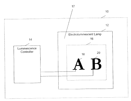
[0040] A
block diagram of an electroluminescent sign 10 is exemplified
in FIG. 1. The electroluminescent sign 10 comprises a substrate with an
illuminatable image, that may be referred to as electroluminescent lamp 12,
electrically coupled or attached, preferably removably coupled or attached, to
a luminescence controller 14. The luminescence controller 14 applies voltage
to the electroluminescent lamp 12 to illuminate an image 16 formed on the
electroluminescent lamp 12. Luminescence controller 14 may be any
controller capable of receiving and storing the instructions for operating the
lamp 12 and providing the commands to the lamp 12. Accordingly
luminescence controller 14 comprises a processor, preferably programmable,
and data storage. Any processor and data storage mechanism known in the
arts may be used.
[0041] As
exemplified in FIG. 1, the image 16 is shown as comprising
the letters "A" and "B". The image 16 may be divided into a number of
illuminating sections 18, 20 on one or more illuminating image layers 34, that
are individually coupled to the luminescence controller 14, and are preferably
selectively controlled by luminescence controller 14. An illuminating section
is
a part of the lamp that is electrically isolated from other illuminating
sections of
lamp 12 so that it may be individually illuminated. Accordingly, luminescence
controller 14 may individually control, e.g., the time, duration and/or
intensity
of illumination of each illuminating section. In FIG. 1 the first illuminating
section 18 comprises the letter "A" and the second illuminating section 20
comprises the letter "B".
This configuration allows the luminescence
controller 14 to separately control/illuminate the illuminating sections 18,
20.
Accordingly, luminescence controller 14 may provided provide differing
amounts of voltage to sections 18, 20 and/or may illuminate sections 18 and
20 for differing amounts of time and/or may illuminate them sequentially or in
any pattern, thereby causing one or more of them to, e.g., flash. It will be
appreciated that letters "A" and "B" may each comprise a plurality of
illuminating sections. Alternately or in addition, background 17 on which
CA 02734062 2011-02-14
WO 2010/020034 PCT/CA2009/001101
letters "A" and "B" are provided may be non-illuminating or may comprise one
or more illuminating sections. Accordingly, a sign may comprise any desired
number of illuminating sections and, optionally, one or more non-illuminating
section. A non-illuminating section is a part of lamp 12 that is not
illuminated
5 and may have an image printed thereon.
[0042] The voltage required to illuminate each illuminating section
to a
particular degree of illumination is dependent on the size of the illuminating
section and the colour of the electroluminescent material. The brightness may
be increased by applying more voltage, but at some point it may reach a
10 saturation point. The average brightness is roughly proportional to the
frequency up to at least 5 kHz, and also depends on the waveform of the
applied voltage.
[0043] The luminescence controller 14 may comprise a memory or
other similar storage device that stores electrical configuration data, e.g.,
a
command or a sequence of commands to control the illumination of the
electroluminescent lamp 12 and a processor to issue the command or
commands. The sequence of commands may include which of the illuminating
sections to illuminate when, for how long, and/or at what brightness. For
example, say, as exemplified, that image 16 comprises two illuminating
sections 18, 20 as shown in FIG. 1. The sequence of commands may include
the following instructions: (a) illuminate section "A" for 5 seconds, (b)
illuminate section "B" for 10 seconds, (c) illuminate sections "A" and "B" for
3
seconds, and (d) repeat. In one embodiment the sequence of commands
may comprise a series of voltage settings. The memory or other similar
storage device may be configurable (e.g., reprogrammable or replacable) so
that the sequence of commands may be updated or modified at a later date.
[0044] The exploded view of an electroluminescent lamp 12 is
exemplified in FIG. 2. The electroluminescent lamp 12 is comprised of a
substrate 30 and a number of layers 32, 34, 36, 38 formed thereon. The
CA 02734062 2011-02-14
WO 2010/020034 PCT/CA2009/001101
11
layers may be formed on the substrate 30 through any known process such
as extrusion through a slot die, or by screen-printing. In the embodiment
exemplified in FIG. 1, the electroluminescent lamp 12 is comprised of a front
electrode layer 32, an electroluminescent or illuminating image layer 34, a
dielectric layer 36, a rear electrode layer 38 and preferably an encapsulation
layer 40. When a voltage is applied across the front and rear electrode layers
32 and 38, the electroluminescent layer 34 is activated and emits light.
[0045] The substrate 30 acts as the base of the electroluminescent
lamp 12 and may be comprised of any suitable transparent or translucent
material such as glass or plastic. The substrate 30 may be rigid or flexible
(e.g., 2 ¨ 5 mil thick). The substrate provides the support for the remaining
layers. Substrate 30 has an outer face 31 which is the outer face exposed to a
viewer. A non-illuminating image layer 42 may be printed directly on substrate
30 and/or may be mounted on substrate 30, such as being laminated thereto.
Accordingly, in one embodiment, layers 30 and 42 may comprise a single
element, e.g., a standard plastic sheet on which a non-illuminating image is
printed. The non-illuminating layer has at least one section that is design or
intended to be illuminated by illuminating image layer 34.
[0046] Preferably, the next layer is the front electrode layer 32.
The
front electrode layer 32 is comprised of suitable optically transparent and
electrically conductive material such as indium-tin-oxide (ITO). This layer
may
be a thin coating applied to the inner face (the face opposite to outer face
31,
of substrate 30.
[0047] The electroluminescent or illuminating image layer 34 is
formed
on the rear face of the front electrode layer 32 and forms the image to be
illuminated (e.g. illuminating sections 18, 20). The electroluminescent layer
34
may be made of any suitable phosphor such as copper, activated zinc sulfide,
or manganese activated zinc sulfide.
CA 02734062 2011-02-14
WO 2010/020034 PCT/CA2009/001101
12
[0048] Where the image 16 is divided into different illuminating
sections
(i.e. 18, 20), each of the layers 32, 34, 36, 38 of the electroluminescent
lamp
12 may be formed in the shape of the illuminating sections provided the
electrode layers 32, 38 are electrically isolated from each other. For
example,
in FIG. 1 the image 16 is divided into two illuminating sections 18, 20, the
"A"
on substrate 30 being illuminated by illuminating section 18 and the "B" on
substrate 30 being illuminated by illuminating section 20. In this case, there
are two portions that are formed on front electrode layer 32. One portion is
exemplified as being formed in the shape of a rectangle that, when the sign is
assembled, is positioned such that the "A" on layer 42 is positioned on top of
illuminating section 18. The other portion is exemplified as being be formed
in
the shape of the "B" of layer 42 and positioned such that the "B" on layer 42
is
positioned on top of illuminating section 20. These illuminating sections
would
be mounted, e.g., printed, on the rear face of front electrode layer 32. The
layers would be spaced apart as shown in FIG. 1 such that illumination of
section 18 would not cause illumination of section 20 (i.e. they are
electrically
isolated from each other). It will be appreciated that sections 18, 20 may
abut,
in which case an insulation layer is preferably provided between adjacent
surfaces if the sections are sufficiently close such that electricity may,
e.g., arc
from one to the other. It will be appreciated that, if the entire image 16 is
to be
illuminated, the layer may extend over the entire layer 32, as represented by
the dotted line of illuminating image layer 34.
[0049] Where the image 16 contains a plurality of colors, the image
16
may be divided into a number of illuminating sections 18, 20, wherein, for
example, each illuminating sections represents a separate color. Each of
these image layers may be separately applied to the rear surface of front
electrode layer 32 such as by printing using a plurality of masks or screens.
[0050] After the electroluminescent of illuminating image layer 34
preferably is the dielectric or insulating layer 36. The dielectric layer 36
may
CA 02734062 2011-02-14
WO 2010/020034 PCT/CA2009/001101
13
be comprised of electrically insulating material that provides a barrier to
the
flow of electricity. Suitable insulating material includes conventional
dielectric
powders, such as white dielectric powder, in a suitable binder. The insulating
layer may be applied over the entire rear surface of electrode layer 32, such
that it overlies the illuminating sections and the front electrode as
represented
by the dotted outline of insulating layer 36. Alternately, it may be applied
over
only the illuminating sections and the portion of front electrode 32 on which
the rear electrode 38 will be provided.
[0051] The rear
electrode layer 38 is preferably formed on the dielectric
layer 36 and may be comprised of any suitable electrically conductive
material. The rear electrode layer 38 may be comprised of the same material
as the front electrode layer 32, such as ITO, or a different material. For
example, the rear electrode layer 36 may be comprised of a suitable opaque
material such as a silver, gold or graphite-based material.
[0052] In other
embodiments the electroluminescent lamp 12
comprises additional layers. For example, the electroluminescent lamp 12
may further comprise an encapsulation layer 40 that acts as a water barrier to
protect the electroluminescent layer 34 from atmospheric moisture.
[0053] It will be
appreciated that electroluminescent lamp 12 may be of
various other
constructions and that various aspects of this invention may be
used with any such construction.
[0054] Reference is
now made to FIG. 3, in which a block diagram of a
system 100 for developing an electroluminescent sign 10 is exemplified. The
system 100 includes an image file 115, a workstation 110 and an
electroluminescent lamp generator 165, which co-operate to develop an
electroluminescent sign 10.
[0055] The image file
115 may be a vector-based graphics file that
represents the image to be displayed on the electroluminescent sign 10. In a
vector-based graphics file the image is defined by mathematical descriptions,
CA 02734062 2011-02-14
WO 2010/020034 PCT/CA2009/001101
14
as opposed to individual pixels. Suitable vector-based graphics file formats
include, but are not limited to, EPS (Encapsulated PostScript), PDF (Portable
Document Format), WMF (Windows Metafile), SVG (Scalable Vector
Graphics) and VML (Vector Markup Language). The image file 115 may be
generated by an artist using a vector-based graphics editor and then loaded
into the workstation 110. It will be appreciated that the image file may be
obtained from any source, e.g., an existing commercial advertisement, that
may be a picture that is scanned to produce a data file or obtained as a data
file.
[0056] As exemplified, the workstation 110 includes a memory 135, an
image processor 120, a voltage mapping module 125 and a display 180. The
memory 135 stores the image file 115 and may comprise volatile (e.g. random
access memory (RAM)) and/or non-volatile memory (e.g. read only memory
(ROM)).
[0057] The image processor 120 is coupled to the memory 135 and the
display 180, and is configured to retrieve the image file 115 and divide the
corresponding image into an illuminating image layer and a non-illuminating
image layer or a plurality of image layers optionally with one or more non-
illuminating layers. The non-illuminating image layer(s) is obtained as non-
illuminating image data, which may subsequently be used to print the non-
illuminating image layer, with or without any distortion. Typically an
operator
will input which sections of the image are to be illuminated and which are not
to be illuminated. The processor will then divide the image into illuminating
and non-illuminating layers based in the input received from the operator.
The sections of the image that will not be illuminated will typically form the
non-illuminating image layer, although other non-illuminating layers may be
provided separately. The sections of the image that will be illuminated may
be further subdivided into a plurality of illuminating image layers, each of
which contains one or more illuminating sections. Each illuminating image
CA 02734062 2011-02-14
WO 2010/020034 PCT/CA2009/001101
layer may represent a different color used in the image. For example, as
exemplified in FIG.1 there are two illuminating sections 18, 20, and the first
illuminating section 18 (i.e. the "A") is to be blue and the second
illuminating
section 20 (i.e. the "B") is to be red. One illuminating image layer may
contain
5 all aspects of the illuminating sections that are blue (i.e. the "A") and
another
illuminating image layer may contain all aspects of the illuminating sections
that are red (i.e. the "B"). For example, the illuminating image layer for the
"A"
may be printed using a first screen and the illuminating image layer for the
"B"
may be printed using a second screen. Alternately, the same screen may be
10 used to print both the "A" and the "B". A method for dividing an image
into
illuminating and non-illuminating image layers that may be implemented by
the image processor 120 is described in detail in relation to FIG. 5. In
accordance with this aspect, the image processor 120 is also configured to
generate voltage mapping information from the image file 115 to be used by
15 the voltage mapping module 125. The voltage mapping module may
determine the size of the illuminating section and calculate a required
voltage
based on the size of the section and a desired level of illumination (e.g.,
the
voltage data).
[0058] The voltage mapping module 125 is coupled to the image
processor 120 and the display 180, and may use the voltage mapping
information generated by the image processor 120 to generate timing
configuration data, which defines the timing of the illumination of the
electroluminescent sign 10. A method of generating timing configuration data
is described in relation to FIG. 8. From the timing configuration data the
voltage mapping module 125 generates a sequence of commands to control
the illumination of the electroluminescent sign 10. Voltage mapping module
125 may contain data to alternately, or in addition, control the level of
illumination and/or the sequence of illumination of different illuminating
sections 18, 20.
CA 02734062 2011-02-14
WO 2010/020034 PCT/CA2009/001101
16
[0059] The electroluminescent lamp generator 165 may be an
amalgamation of individual components that together generate an
electroluminescent lamp 12. The electroluminescent lamp generator 165
receives the data on the illuminating and optional non-illuminating image
layers from the image processor 120 and generates an electroluminescent
lamp 12 having the required image. In the embodiment shown in FIG. 3, the
illuminating image layers of the required image may be printed on substrate
30 by known silk-screening techniques to generate an electroluminescent
lamp 12. However, other suitable methods, e.g. ink jet printing, vapour
deposition, lamination of a separately prepared layer, of depositing the
illuminating image layers on the substrate 30 may also be used.
[0060] In the silk-screening embodiment shown in FIG. 3, the
electroluminescent lamp generator 165 includes a screen maker 130, a silk-
screen machine 140, a shift repair module 145 and a lamination module 170.
The screen maker 130 comprises equipment that is automatically or manually
operable to generate a screen, such as a silk-screening screen. The screen
maker 130 receives the image data for the illuminating image layers
generated by the image processor 120 and in accordance with standard silk-
screening techniques, generates one screen for each layer. Any other method
known in the art for producing a plurality of areas of electroluminescent
material on a support surface may be sued.
[0061] The screen maker 130 may receive the image data for the
illuminating image layers from the image processor 120 over a data network,
such as an Ethernet network, a wireless network or a combination of the two.
Alternatively the screen maker 130 may receive the image data for the
illuminating image layers via a transportable storage medium readable by the
screen maker 130 such as a portable memory stick, diskette or CD. The
mesh size of each screen may be based on the ink being used for that layer,
CA 02734062 2011-02-14
WO 2010/020034 PCT/CA2009/001101
17
including its mess size, as is known in the screen printing art.. The ink used
for each layer may be specified by the image processor 120.
[0062] The silk-screen machine 140 comprises equipment that is
automatically or manually operable to generate an electroluminescent lamp
12 using silk screening techniques. Any silk-screen machine 140 may be
used. The silk-screen machine 140 receives the screens created by the
screen maker 130 and the substrate 30 that is to be used at the base of the
electroluminescent lamp 12.
[0063] After receiving the screens and the substrate 30, which may
be
precoated with front electrode layer 32 if front electrode layer 32 is not
applied
by silk screen machine 140, the silk-screen machine 140 applies layers of ink
to the substrate 30 using the screens. In accordance with the embodiment of
FIG. 3, all illuminating layers are printed using a silk-screen machine 140.
In
one embodiment there are four types of ink applied to the substrate ¨
phosphor ink, insulation or dielectric ink, and conductive ink. The phosphor
ink contains the electroluminescent material and is used to create the
electroluminescent layer 34 of the electroluminescent lamp 12. As described
above, several layers of phosphor ink may be applied to the substrate 30. For
example, all illuminating sections of a particular colour may be applied in
using a single screen and may be considered a single layer, albeit a
discontinuous layer. The insulation or dielectric ink is an electrically
insulating
material that provides a barrier to the flow of electrons and used to form the
dielectric layer 36. The conductive ink can comprise silver, gold or graphite-
based ink that is electrically conductive. In another embodiment encapsulate
ink may be applied to provide a water barrier that protects the phosphor ink
from moisture in the atmosphere.
[0064] After each layer of ink is applied to the substrate 30, the
substrate 30 may be heated at a specified temperature for a specified time to
drive off the ink's solvent. It will be appreciated that the substrate may be
CA 02734062 2011-02-14
WO 2010/020034 PCT/CA2009/001101
18
heated after two or more non-overlapping layers are applied. The substrate 30
may be heated in an oven or other suitable heating device. The specified
temperature may be 130 degrees Celsius, for example, and the specified time
may be 20 minutes, for example. Any desired temperature may be used
provided it is sufficiently high to drive off the solvent but sufficiently low
so as
not to degrade the ink of the substrate.
[0065] The optional shift repair module 145 is a device or
collection of
devices that align, e.g., the original non-illuminating image layer with the
illuminating image layers printed on the substrate 30. The shift repair module
145 receives the electroluminescent lamp 12 generated by the silk-screen
machine 140 and the illuminating and optional non-illuminating image layers
generated by the image processor 120. The shift repair module 145 may
receive the illuminating and non-illuminating image layers from the image
processor 120 over a data network, such as an Ethernet network, a wireless
network or a combination of the two. Alternatively the shift repair module 145
may receive the illuminating and non-illuminating image layers via a
transportable storage medium readable by the shift repair module 145 such
as a portable memory stick, diskette or compact disc (CD).
[0066] If the non-illuminating image layer 42 is not printed onto
substrate 30, then shift repair module 145 is optionally used to align the non-
illuminating image layer 42 with the illuminating image layers printed on
substrate 30. This alignment is desirable (although not necessarily required)
where heating the substrate during the silk-screening process causes
distortions in the substrate 30, which distorts the printed illuminating image
layers. This distortion problem can be rectified by using water-based inks.
However, this solution cannot be used for a phosphor ink due to its
sensitivity
to water. Accordingly, to be able to correctly align the non-illuminating
image
layer with the printed illuminating image layers, the non-illuminating image
layer must be similarly distorted. A method for aligning an original non-
CA 02734062 2011-02-14
WO 2010/020034 PCT/CA2009/001101
19
illuminating image layer with the corresponding printed illuminating image
layers that may be implemented by the shift repair module 145 is described
below with reference to FIG. 7.
[0067] In
one embodiment, the shift repair module 145 includes a
scanner and a processor. The
scanner generates a digital image
representing the illuminating image layers printed on the substrate 30. Any
scanner known in the art may be used. The digital image is then transferred to
the processor. The digital image may be transferred from the scanner to the
processor through a data network, such as an Ethernet or wireless network,
or through use of removable storage media, such as a memory key, that is
written to by the scanner and read by the processor. The processor then
compares the digital image with the original illuminating image layer (e.g.
image file 115) to determine the distortion. Once the distortion is
determined,
the processor applies the distortion to the data representing the non-
illuminating image layer so that it is aligned with the digital image. A
suitably
distorted non-illuminating image layer may then be printed on a second
transparent or translucent substrate, e.g. by silkscreen machine 140, so as to
be laminated on to substrate 30 or printed directly on front surface 31 of
substrate 30. The distorted non-illuminating image layer may be printed using
any printing device known in the printing arts.
[0068] The
lamination module 170 is a device or a collection of devices
that apply the original non-illuminating image layer or the distorted non-
illuminating image layer to front surface 31 of substrate 30. The lamination
module 170 receives the electroluminescent lamp 12 generated by the silk-
screen machine 140 and preferably the distorted non-illuminating image layer
generated using data from the shift repair module 145. After receiving the
electroluminescent lamp 12 and a non-illuminating image layer, the lamination
module 170 applies the printed image to the electroluminescent lamp 12
through a lamination process.
CA 02734062 2011-02-14
WO 2010/020034 PCT/CA2009/001101
[0069] The electroluminescent lamp 12 is then operably associated
with a luminescence controller 14, for example by electrical and physical
attachment, connection, or coupling, which is preferably releasable, to form
an
electroluminescent sign 10. The luminescence controller 14 supplies voltages
5 to parts of the electroluminescent lamp 12 to cause those parts to
phosphoresce and thereby illuminate the illuminating portions of the
electroluminescent lamp 12. The illuminating portions of the
electroluminescent lamp 12 may be illuminated according to a predetermined
timing and location pattern, which is set by the sequence of commands
10 generated by the voltage mapping module 125.
[0070] It will be appreciated that luminescence controller 14 and
electroluminescent lamp 12 may each be separately mounted to a suitable
frame and electrically connected together by electrical conduits in the frame.
For example, the frame may have a plurality of ports that are contacted by
15 electrodes in layer 38 and by the leads of a controller 14. Alternately,
electrodes in layer 38 may be directly connected to controller 14.
[0071] Reference is now made to FIG. 4, in which a flowchart of a
method of developing an electroluminescent sign 10 using system 100 is
exemplified. In the first step 210 an image file 115 is received. As stated
20 above, the image file 115 may be a vector-based image file that
represents
the image to be displayed on the electroluminescent sign 10. The image file
115 is typically loaded into the workstation 110 and stored in the workstation
memory 135. Once the image file has been received, at step 220 the image
file 115 is divided into illuminating and optional non-illuminating image
layers.
A method for dividing an image file 115 into illuminating and non-illuminating
image layers is described below with reference to FIG. 5. During this step
220, the image processor 120 also generates voltage mapping information
from the image file 115 to be used by the voltage mapping module 135.
CA 02734062 2011-02-14
WO 2010/020034 PCT/CA2009/001101
21
[0072] Once the image file 115 has been divided into illuminating
and
non-illuminating image layers, at step 230 screens to be used in a silk-
screening process are generated for each illuminating image layer, and
optionally for the non-illuminating layers. In system 100, the silk-screens
are
generated by the silk-screen maker 130. Specifically, the silk-screen maker
130 receives the illuminating art file generated by the image processor 120
and one screen is generated for each layer of the illuminating art file.
[0073] After the screens have been generated in step 230, in step
240
the electroluminescent lamp 12 is generated. In one embodiment the
electroluminescent lamp 12 is generated from the screens using well-known
silk-screening techniques. A method for generating a sign using silk-
screening techniques is described below with reference to FIG. 6.
[0074] In addition to generating a set of screens for the silk-
screening
process, the information generated in step 220 is also used in step 250 by the
voltage mapping module 125 to generate, e.g., timing, sequence and/or
voltage data. The timing data defines the timing of the illumination of the
illuminating sections of the electroluminescent lamp 12. The voltage data
defines the intensity of the illumination of the illuminating sections of the
electroluminescent lamp 12 and comprises voltages values representing
voltages transmitted to an illuminating section 18, 20. The sequence data
defines the sequence of the illumination of the illuminating sections of the
electroluminescent lamp 12. Accordingly, this configuration data may set out
which illuminating sections of the electroluminescent lamp 12 will be
illuminated when, for how long and at what brightness. For example, if the
image 16 has two illuminating sections 18, 20 as shown in FIG. 1, the timing
configuration data may specify at specific points in time which of the
illuminating sections are illuminated and at what intensity. A method for
generating configuration data that may be implemented by the voltage
mapping module 125 is described below with reference to FIG. 8.
CA 02734062 2011-02-14
WO 2010/020034 PCT/CA2009/001101
22
[0075] Once the configuration data has been generated, in step 260
the
voltage mapping module 125 converts the configuration data into a sequence
of commands to control the illumination of the electroluminescent lamp 12. In
one embodiment the sequence of commands comprise a sequence of voltage
levels for each illuminating section of the electroluminescent lamp 12. In one
embodiment the voltage levels are automatically generated by the voltage
mapping module 125 based on the size of the illuminating sections. A higher
voltage level will be required to illuminate to the same brightness an
illuminating section with a greater area than one with a smaller area.
[0076] After the sequence of commands is generated in step 260, at
step 270 the commands are loaded onto the luminescence controller 14.
Once the commands are loaded onto the luminescence controller 14, the
electroluminescent lamp 12 is physically and electrically attached, coupled or
connected, at step 280, to the luminescence controller 14 to form the
electroluminescent sign 10. Where the image 16 is comprised of a plurality of
illuminating sections (i.e. 18, 20), each illuminating section of the
electroluminescent lamp 12 is separately attached, coupled or connected to
the luminescence controller 14.
[0077] Reference is now made to FIG. 5, in which a flowchart of a
method 220 for dividing an image into illuminating and non-illuminating layers
is exemplified. In the first step 310 the image processor 120 retrieves the
image file 115 from the memory 135.
[0078] After the image file 115 is retrieved, at step 320 the image
processor 120 displays the image contained in the image file 115 on the
display 180.
[0079] Then, at step 330 the image is divided into illuminating
sections
and optional non-illuminating sections. Typically an operator will identify
which sections of the image are to be illuminated and may determine which
parts are to be separate illuminating sections. For example, the operator may
CA 02734062 2011-02-14
WO 2010/020034 PCT/CA2009/001101
23
be provided tools for selecting sections of the image shown on the display 180
and identifying them as being illuminating sections. Those sections of the
image that are not identified as illuminating section may form the non-
illuminating image layer. As was described above in relation system 100, the
non-illuminating image layer may be applied (i.e. laminated) to the
electroluminescent lamp 12 in the last step of the process.
[0080] Then, at step 340 the image processor 120 divides the
illuminating sections of the image into image data representing at least one
image layer. In one embodiment the illuminating sections of the image are
divided into layers based on color. For example, all red areas of the
illuminating sections may be placed in one illuminating image layer and all
blue areas of the illuminating sections may be placed in another illuminating
image layer. In this embodiment, the number of illuminating layers will be
based on the number of different colors in the illuminating sections of the
image. The layers are then subsequently used to create the screens for the
silk-screening processing. For example, the red illuminating image layer will
be used to create the screen to be used for the red ink and the blue
illuminating image layer will be used to create a screen to be used to apply
the blue ink. It will be appreciated that a plurality of illuminating sections
of the
same colour may also be produced.
[0081] Finally, at step 350 the image processor 120 stores the image
data in an art file referred to as the illuminating art file and stores the
non-
illuminating image layers in an art file referred to as the non-illuminating
art
file. These files (e.g., PS, EPS, giff, tiff, jpg, png, psd) are used to
produce the
screen for the silk screening process In addition to generating the
illuminating
and non-illuminating art files, the image processor 120 may also the voltage
mapping art file.
[0082] Reference is now made to FIG. 6, in which a method 240 for
generating an electroluminescent lamp 12 using silk-screening techniques is
CA 02734062 2011-02-14
WO 2010/020034 PCT/CA2009/001101
24
exemplified. The method 240 preferably involves three steps ¨ the silk-
screening step 410, the shift alignment step 420 and the lamination step 430.
[0083] In
the silk-screening step 410, the silk-screen machine 140
prints the illuminating image layers on the substrate 30. Specifically, the
silk-
screen machine 140 uses the screens generated by the screen maker 130 in
step 230 of method 200 to apply layers of ink to the substrate 30. As noted
above, after each layer of ink is applied to the substrate 30, the substrate
30
may be heated to remove the liquid component of the ink.
[0084] In
the optional shift alignment step 420, the shift repair module
145 aligns the original non-illuminating image layer with the illuminating
image
layers printed on the substrate 30. As noted above, this step is advantageous
where heating the substrate 30 distorts the substrate 30, which accordingly
distorts the illuminating image layers printed on the substrate 30. A
preferred
method for aligning the printed illuminating image layers with the original
non-
illuminating image layer is described below with reference to FIG. 7.
Essentially, the exemplified shift repair module 145 compares the printed
illuminating image layers to the original illuminating image layers to
determine
the distortion, and then applies the same distortion to the non-illuminating
image layer to generate a distorted non-illuminating image layer.
[0085] Once a
distorted non-illuminating image layer has been
generated, in the laminating step 430, the distorted non-illuminating image
layer is applied to the inked substrate (i.e. lamp) by the lamination module
170. In one embodiment the lamination module 170 prints the distorted non-
illuminating image layer using an ink-jet printer or other similar device and
laminates it to the electroluminescent lamp 12. In another embodiment, a
printed non-illuminating layer 42 is applied to outer surface 31 of substrate
30.
[0086]
Reference is now made to FIG. 7, in which a method 420 for
aligning printed illuminating image layers with a corresponding non-
illuminating image layer is exemplified. At step 510 the electroluminescent
CA 02734062 2011-02-14
WO 2010/020034 PCT/CA2009/001101
lamp 12 is scanned to generate an electronic image of the illuminating image
layers printed on the substrate 30. The scanning may be accomplished with a
blueprint scanner or other similar scanning devices.
[0087] At
step 520, the electronic image of the illuminating image layers
5 printed on the substrate 30 is compared to the illuminating image layers
in the
original illuminating art file, e.g., an image file produced by image
processor
120, to determine the distortion pattern (also referred to as a shift
pattern).
[0088] Once
the distortion or shift pattern is determined, at step 530 the
original non-illuminating image layer is similarly distorted and saved in a
new
10 non-illuminating art file.
[0089]
Reference is now made to FIG. 8, in which a method 250 for
generating configuration data is exemplified. As previously mentioned, the
configuration data may set out which illuminating sections of the image will
be
illuminated when, for how long and at what brightness. In the first step 610
of
15 method 250 the voltage mapping module 125 receives the voltage mapping
art file from the image processor and displays the corresponding image on the
display 180. In one embodiment, the illuminating sections of the image are
identified on the display 180 and distinguished from the non-illuminating
sections.
20 [0090]
In step 620 the operator identifies, e.g., the length of time the
illumination sequence will run. For
example, the user may want an
illumination sequence to run for 30 seconds and then repeat. The length of
time the illumination sequence will run will be referred to as the
illumination
time period.
25 [0091]
After the illumination time period is determined, at step 630 the
illumination period is divided into a number of equal or unequal time
segments. The number and size of the time segments may be automatically
selected by the voltage mapping module 125 or may be manually selected by
the operator. Once the time segments have been defined, the operator
CA 02734062 2013-06-04
26
..
assigns an illumination intensity value to each time segment for each
illuminating
section (i.e. 18, 20) of the image 16. The higher the illumination intensity
value,
the brighter the illumination. In one embodiment an illumination intensity
value of
zero indicates that the associated illuminating section is "off" or not
illuminated.
[0092] Once the operator has entered illumination intensity values for each
illuminating section of the image, the voltage mapping module 125 preferably
generates a simulation of electroluminescent sign 10 using the selected
illumination intensity values. The simulation is then shown to the operator on
the
display 180. The operator can then determine if they are satisfied with the
operation of the electroluminescent sign 10 using the selected illumination
intensity value. If the operator is not satisfied, then the operator may be
given
the option to edit the illumination intensity setting and then run another
simulation. If the operator is satisfied with the simulation, then the
illumination
intensity values are converted to a sequence of commands to control the
illumination of the illumination sections of the electroluminescent lamp 12.
[0093] It will be appreciated that the intensity values
may be determined
regardless of whether timing data is produced. Further, in any embodiment, the
voltage mapping module 125 may automatically produce the voltage
configuration data.
[0094] The scope of the claims should not be limited by the preferred
embodiments and examples, but should be given the broadest interpretation
consistent with the description as a whole.