Note: Descriptions are shown in the official language in which they were submitted.
CA 02734435 2011-02-16
WO 2010/023570 PCT/IB2009/053176
-1-
PARTIAL DISCHARGE MONITOR
BACKGROUND OF THE INVENTION
THIS invention relates to high voltage electrical or power systems and in
particular to a method and device for monitoring partial discharges in high
voltage electrical or power systems.
The insulation of high voltage, typically three phase, electrical or power
systems are often susceptible to impulses which occur therein. These
impulses are typically due to discharges across inhomogeneous
boundaries within the high voltage electrical or power system, such as gaps
in insulation of cables, or the like. It will be appreciated that these
discharges are often partial discharges within the high voltage electrical
insulation.
It is therefore an object of the present invention at least to provide a
method
and a system to monitor or detect partial discharges occurring in high
voltage three phase electrical or power systems.
CA 02734435 2011-02-16
WO 2010/023570 PCT/IB2009/053176
-2-
SUMMARY OF THE INVENTION
According to a first aspect of the invention there is provided a method of
monitoring partial discharges occurring in an electrical system, the method
comprising:
defining a low trigger level and a high trigger level, the low and the
high trigger levels being amplitude levels for electrical pulses,
wherein the high trigger level is a higher amplitude than the low
trigger level;
defining a minor time frame period;
monitoring at least one phase of the electrical system for an
occurrence of a pulse within the minor time frame;
detecting a peak amplitude of a pulse occurring in the electrical
system within the minor time frame;
determining if the detected peak amplitude of the pulse exceeds the
lower trigger level and/or the higher trigger level;
assigning a pulse number to the pulse if the peak amplitude of the
pulse exceeds the lower trigger level and/or the higher trigger level;
capturing the pulse, or information associated therewith, if the pulse
number associated with the pulse is less than a predetermined
pulse number threshold in the minor time frame;
applying a moving time trigger offset, such that:
if a pulse exceeds the low trigger level but not the high
trigger level and the pulse number equals a predetermined
CA 02734435 2011-02-16
WO 2010/023570 PCT/IB2009/053176
-3-
number of pulses then recording the time value within the
minor time frame at which this occurs and ceasing to capture
pulses exceeding the low trigger level but not the high trigger
level until after this time value in a following minor time
frame; and
resetting the time value of the moving time trigger offset to
zero and starting to capture pulses for the next minor time
frame for pulses exceeding only the low trigger level after the
moving time trigger offset value equals the value of the
minor time frame; and
storing the captured pulses in a memory device.
The method may comprise selecting the pulse number threshold, the pulse
number threshold being a maximum number of pulses to be captured in the
minor time frame.
It will be appreciated that assigning a pulse number to the pulse may
comprise incrementing a pulse number counter thereby to keep track of the
number of pulses exceeding the lower trigger level and/or the higher trigger
level in the minor time.
The method may comprise capture pulses on a next cycle at a point at
which the moving time trigger offset stopped on a previous cycle.
The method may comprise capturing pulses, or information associated
therewith, as low-level events or high-level events, wherein low-level events
are deemed to occur if the peak amplitude of the pulse exceeds the lower
trigger level but not the higher trigger level and wherein the high-level
event
is deemed to occur if the peak amplitude of pulse exceeds both low and
high trigger levels respectively.
CA 02734435 2011-02-16
WO 2010/023570 PCT/IB2009/053176
-4-
The method may further comprise:
starting a timer and storing a peak amplitude and sign of a previous
pulse if a peak amplitude of a current pulse at a sample point falls
below that of a previous sample; and
resetting the timer and starting a new timeslice period, if during a
timeout period, the peak amplitude of a current pulse is greater than
the stored peak amplitude of the previous pulse.
According to a second aspect of the invention, there is provided a device
for monitoring and capturing partial discharges occurring in a three phase
electrical system, the device comprising:
a peak detector for detecting peak amplitudes of pulses occurring in
the electrical system;
a trigger module arranged to:
determine if the detected peak amplitude of the pulse
exceeds a lower trigger level and/or the higher trigger level,
the low and the high trigger levels being amplitude levels for
electrical pulses, wherein the high trigger level is a higher
amplitude than the low trigger level;
assign a pulse number to the pulse if the peak amplitude of
the pulse exceeds the lower trigger level and/or the higher
trigger level;
capture the pulse, or information associated therewith, if the
pulse number associated with the pulse is less than a
predetermined pulse number threshold in a minor time frame
CA 02734435 2011-02-16
WO 2010/023570 PCT/IB2009/053176
-5-
and;
a database in which a plurality of pulses, or information associated
therewith, captured by the trigger module is stored.
The device may comprise a processor arranged at least to apply a moving
time trigger offset. It follows that the processor may be configured to:
record a time value within the minor time frame at which the peak
amplitude of the pulse exceeds the low trigger level but not the high
trigger level and the pulse number equals the predetermined pulse
number threshold;
cease capturing pulses, or information associated therewith, for
those pulses with peak amplitudes exceeding the low trigger level
but not the high trigger level until after the time value in a following
minor time frame; and
reset the time value of the moving time trigger offset to zero and
capturing pulses for the next minor time frame for pulses having
peak amplitudes exceeding only the low trigger level after the
moving time trigger offset value equals the value of the minor time
frame.
The device may optionally comprise a co-ordinate converting module
arranged to convert a vector from Cartesian co-ordinates to polar co-
ordinates.
BRIEF DESCRIPTION OF THE DRAWINGS
Figure 1 shows a schematic interface diagram of a partial discharge
monitoring (PDM) device, in accordance with an example
CA 02734435 2011-02-16
WO 2010/023570 PCT/IB2009/053176
-6-
embodiment, interfacing with a high voltage three-phase
electrical or power system;
Figure 2 shows a graphical representation of a typical discharge
pulse;
Figure 3 shows a functional block diagram of a PDM device able to
interface with one sensor of the system shown in Figure 1;
Figure 4 shows a schematic block diagram of the PDM device of
Figure 3 in greater detail;
Figure 5 shows a schematic interface diagram of a portion of the PDM
device of Figure 4 in greater detail; and
Figure 6 shows a high level flow diagram of a method in accordance
with an example embodiment
DESCRIPTION OF PREFERRED EMBODIMENTS
In the following description, for purposes of explanation, numerous specific
details are set forth in order to provide a thorough understanding of an
embodiment of the present disclosure. It will be evident, however, to one
skilled in the art that the present disclosure may be practiced without these
specific details.
Referring to Figure 1 of the drawings, a partial discharge monitoring (PDM)
device 10 is communicatively coupled to a high voltage electrical or power
distribution system 12, for example a three-phase power supply distribution
system, via an input multiplexor 14 to monitor the system 12 for partial
discharge pulses of a similar type illustrated in Figure 2. The multiplexor is
in turn connected to the system 12 by way of a plurality of sensors 16.
Each sensor 16 is typically in the form of a capacitor and a resistor to
CA 02734435 2011-02-16
WO 2010/023570 PCT/IB2009/053176
-7-
ground, or in other words a single pole high pass filter. In an example
embodiment, a pair of sensors 16 is provided for each phase 1, 2 and 3 of
the three-phase power system 12 such that there are six inputs to the
multiplexor 14. A known distance separates the two sensors 16 per phase
this allows an indication of position of the source by monitoring the
direction
of travel of a pulse.
An example embodiment of a partial discharge monitoring (PDM) device 10
for use with a single phase is shown in Figure 3. It will be noted that the
PDM device 10 is a single input module, which is typically arranged to
receive an input from any one of the six sensors 16. The device 10 does
not capture all the events in a mains cycle, but progressively builds up a
picture of all the events in a cycle as will be described in more detail
below.
For ease of explanation, two time frames are defined in this specification
firstly a time slice, and secondly a minor time frame. A time slice is an 80
ps time frame which is the time resolution for display of data in a scatter
plot generated by an attached computer. A minor time frame on the other
hand is a 20 ms time frame, which is equivalent to one cycle at 50 Hz. It
follows that a minor time frame typically consists of 250 time slices.
In the example embodiment, the pulse characteristics of the PDM device 10
include a maximum frequency of 250 MHz, a maximum pulse length of 4 ps
and a minimum rise time around 10 ns.
Referring to Figure 3 of the drawings, the PDM device 10 includes a
plurality of components or modules which correspond to the functional
tasks to be performed by the device 10. In this regard, "component" or
"module" in the context of the specification will be understood to include an
identifiable portion of code, computational or executable instructions, data,
or computational object to achieve a particular function, operation,
processing, or procedure. It follows that a component or module need not
be implemented in software; a component or module may be implemented
in software, hardware, or a combination of software and hardware. Further,
CA 02734435 2011-02-16
WO 2010/023570 PCT/IB2009/053176
-8-
the components or modules need not necessarily be consolidated into one
device but may be spread across a plurality of devices.
In particular, the PDM device 10 includes a peak detector 20 for detecting
peak amplitudes of pulses occurring in the electrical system 12. The peak
detector 20 determines the maximum amplitude within the pulse and
passes this along with a valid flag to a trigger module 22 of the PDM device
(described in greater detail below).
The peak detector 20 is in effect a peak tracking architecture. If the
magnitude at a sample point falls below that of the previous sample then a
timer will be started and the magnitude and sign of the previous sample are
stored. If during a timeout period the current magnitude is greater than the
stored value, then the magnitude and sign are stored, the timer is reset and
a new timeout period started. When the timer times out, a valid peak shall
be declared by asserting a peak valid flag.
The peak detector 20 thus detects the peaks of pulses and passes these
onto the trigger module 22 of the PDM device 10 to which it is
communicatively coupled.
The trigger module 22 is arranged to compare peak amplitudes of pulses
occurring in the electrical system with a high trigger level and a low trigger
level. These trigger levels are set within the device and can be reset from
time to time by accessing the trigger module 22. In an example
embodiment, the low trigger level may be 20 mV and the high trigger level
may be 100 mV.
The device 10 is arranged to capture all pulses which have peak
amplitudes above the high trigger level and is also arranged to capture a
predetermined number of pulses which have peak amplitudes above the
low trigger level but below the high trigger level.
CA 02734435 2011-02-16
WO 2010/023570 PCT/IB2009/053176
It will be appreciated that capturing a pulse includes capturing information
indicative or associated with the pulse.
The PDM device 10 also includes a memory in the form of a database or
data store 24 in which the plurality of captured pulses are stored. The
device 10 is arranged to apply a time trigger offset to the low trigger level.
The trigger module 22 is therefore arranged to capture pulses on a next
cycle at the point at which the time trigger offset stopped on the previous
cycle.
Turning now to Figures 4 and 5 of the drawings, the PDM device 10
typically includes a processor 30 typically in the form of a field
programmable gate array (FPGA). It will be noted that in one example
embodiment the peak detector 20 and trigger module 22 are components
or modules provided in the processor 30.
The PDM device 10 is typically mains powered, thus a zero crossing
detector 32 is included within the PDM device 10. The zero crossing
module 32 provides a reference time for the minor time frame. Typically,
only negative to positive transitions are detected.
In one example embodiment, the PDM device 10 is implemented as a
single printed circuit board (PCB) containing all components as illustrated in
Figure 4. Instead, the PDM device 10 may be split between two or more
PCBs for example one PCB containing the input protection 34, buffer
amplifiers 36, relays 38 and relay driver 40 (all described below). The
second PCB then would consist of the entire signal processing hardware.
As mentioned, the PDM device 10 includes input protection modules 34.
The input protection modules 34 provide the electronics of the PDM device
both over-voltage and over-current protection from high-energy spikes
on the inputs from the sensors 16. The input protection modules can
typically withstand a fast 200 V transient.
CA 02734435 2011-02-16
WO 2010/023570 PCT/IB2009/053176
-10-
The PDM device 10 further includes an analogue buffer or buffer amplifiers
36 to provide a high-input impedance at the interface to the electronics.
Due to the signal processing hardware having only one channel, it will be
necessary to select one of the six inputs as the input to the signal
processing hardware. This is done by way of the relays 38 and relay driver
40. In an example embodiment VHF relays are used as the switches.
It will be understood that the relay driver 40 converts control signals from
the processor 30 to a level suitable for switching the relays 38.
The PDM device 10 typically includes an anti-alias filter 42 with following
parameters for example:
C Passband: 250 MHz
C Passband ripple: 0.5 dB
C Stopband: > 375 MHz
C Stopband attenuation: 60 dB
The PDM device 10 includes an analogue-to-digital converter (ADC) 44.
The ADC 44 allows for sampling at 800 Msps. In practice this means that
the PDM device 10 will be a 1 Gsps 8 bit device. It must be mentioned
here that the sampling rate must be commensurate with the maximum
frequency input and the minimum rise time. In general the maximum
frequency content of a signal is no more than 0.4 * FS where F5 is the
sampling frequency. Thus for the PDM device 10, the minimum sampling
frequency will be 625 MHz making the abovementioned sampling
frequency of 800 MHz very suitable.
A serial flash 46 is non-volatile memory required to store the firmware data
for the processor 30.
In the illustrated embodiment, the PDM device 10 includes a 10/100 Local
Area Network (LAN) output 48.
CA 02734435 2011-02-16
WO 2010/023570 PCT/IB2009/053176
-11-
A field upgrade module 50 may also be provided in the PDM device 10.
The module 50 provides the functionality to enable an update of the
firmware of the processor 30 in the field. The new program is typically
transferred to unit via the LAN 48. The new data will be stored temporarily
in SRAM 52, and once all the data has been transferred the complex
programmable logic device (CPLD) 54 will undertake the re-programming
of the serial FLASH 46.
It will be understood that a clock 56 is required, the clock 56 comprising two
clocks i.e. a 800 MHz clock for ADC 44, and 200 MHz system clock for
processor 30.
A power supply unit (PSU) 58 provides voltage conditioning to supply all
the required DC voltages within the PDM device 10. The input to the PSU
58 is at a standard mains supply at 110V or 230V. In an example
embodiment the PSU 58 provides the PDM device 10 with a wide reset
signal.
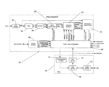
Looking at the processor 30 in more detail with reference to Figure 5, it will
be noted that the processor 30 also includes a plurality of components or
modules as hereinbefore described. In addition to the peak detector 20,
trigger module 24, and database 24, the processor 34 also comprises an
ADC interface 60 to interface with the ADC 44.
The ADC 44 provides some level of de-multiplexing to reduce the data rate
to the processor 30. Typically this is a 2:1 de-mux, which means two
samples are collected and transferred to the processor 30 in parallel, thus
the data rate seen by the processor 30 is half that of the ADC sample rate.
Having regard to the abovementioned sampling rate of 800 Msps, this
means that the processor 30 will receive data at 400 Msps. However, in
the present example embodiment the system clock rate of the processor 30
is unlikely to be at 400 MHz and is typically 200 MHz. Thus the ADC
interface 60 provides a further level of de-multiplexing within the processor
CA 02734435 2011-02-16
WO 2010/023570 PCT/IB2009/053176
-12-
30 so that the input to the remainder of the PDM device 10 will be at the
system clock rate.
The processor 30 also includes a filter 62 to remove DC elements. Also, in
order to determine magnitude and phase of the input signal on a sample-
by-sample basis, the input data is typically converted into an analytical
signal (complex).
It will be noted that the output of the filter 62 are the I and Q components
of
a complex signal.
The processor 30 includes a co-ordinate converting module 64. The co-
ordinate converting module 64 is arranged to convert a vector from
Cartesian co-ordinates to a polar co-ordinate form (magnitude and phase).
The peak detector module 20 as provided in the processor 30 was
hereinbefore described in detail. The trigger module 22 on the other hand
needs more explanation.
As an aside, it will be noted that the trigger levels are capable of being set
by a user via a computer, however, default values are typically provided. In
an example embodiment, the low level trigger can be used to enable
capturing of all events in a minor time frame. It will be noted that in the
context of the specification "event" will be understood to include the
occurrence of a pulse. In this regard, a low-level event is deemed to occur
if the pulse magnitude exceeds the lower trigger level but not the higher
trigger level whilst a high-level event is deemed to occur if the pulse
magnitude exceeds both trigger levels.
As mentioned, not all events but a predetermined number thereof is
captured in a single minor time frame. In particular, a maximum value is
captured. This can be any number from one upward. In this case, ten low
level and ten high level events per cycle are captured. For high level
events, once the maximum value is exceeded during a minor time frame,
CA 02734435 2011-02-16
WO 2010/023570 PCT/IB2009/053176
-13-
capture ceases until the start of the next minor time frame. The next
capture starts at the beginning of the next minor time frame.
For low-level events, a trigger hold-off is typically provided to ensure that
the capture within a cycle resumes where the capture in the previous cycle
finished, having captured the ten events.
It is assumed that the final capture for both high and low level events within
a minor time frame will finish at the end of the minor time frame irrespective
of whether ten pulses have been captured or not.
An example of the above would be as follows. At the start of a minor time
frame (20 mS) a timer is started. Any low level pulses, detected after the
timer has started that exceed the low level trigger and do not exceed the
high level trigger and that occur during this minor time frame are captured,
up to a maximum number of pulses (for example 10 pulses).
If the maximum number of pulses are captured quickly, say in less than 20
ms, then capturing will cease before the end of the minor time frame and
the relative time on the cycle which is represented by the timer value at
which capturing ceases is recorded.
Capturing will only recommence for low level pulses during the next minor
time frame, at the relative time, from the previous minor time frame, at
which capturing ceased, that is the time recorded from the timer. The next
pulse that occurs after this relative time offset, that exceeds the lower
trigger level and not high level trigger, is then recorded.
This process is repeated, for the capturing of groups of 10 pulses, until the
timer value equals the value of the length of a minor time frame. This is
referred to as a moving time trigger offset.
Sometimes only a few pulses, say less than 10, will be captured when the
timer value is very close to the value of the minor time frame. This is
CA 02734435 2011-02-16
WO 2010/023570 PCT/IB2009/053176
-14-
because at the end of the minor time frame capturing will cease, the timer
is reset and starts again and pulse capture will only recommence when the
lower trigger level is again exceeded.
For pulses exceeding the low and high level trigger, during a given minor
time frame, the pulse that exceeds both the low and high level trigger is
captured and stored repeatedly unless there are more than a maximum
number of such pulses captured in the predetermined minor time frame (for
example 20 ms). In the illustrated embodiment the maximum number of
pulses to be captured that exceed the high trigger level is 10 per minor time
frame. The difference between this scenario and the scenario described
above is that once 10 pulses are captured no further pulses are captured
until the next minor time frame. There is no moving time trigger offset
applied to the capturing of pulses that exceed both the low and high trigger
level.
In an example embodiment, the default low trigger level may roughly be 20
mV input level while a default high trigger level may roughly be 100mV
input level.
The trigger module 22 is arranged to compare the valid output from the
peak detector 20 against the two mentioned trigger levels. The comparison
against the low trigger level shall only occur if the low trigger enable
signal
is asserted.
If an event above the trigger levels has occurred then the record number,
an indication as to whether the data is from the low trigger or the high
trigger and a time-stamp is transferred to a database or data store 24 of the
PDM device 10. In addition, a data store signal is asserted to start the
storing of the raw data into an appropriate memory slot in the database 24.
In an example embodiment, typically 4 ps worth of raw data encompassing
the event is captured in the database 24. The data captured preferably
also includes pre-trigger data in order to capture the rise time of the event.
CA 02734435 2011-02-16
WO 2010/023570 PCT/IB2009/053176
-15-
For example with a maximum rise time of 100 ns then -150 ns of pre-
trigger data is captured.
At the end of a minor time frame the captured data and stored data is
optionally transferred to the host computer 18. It follows that the data
transferred includes the time stamp, which will be the time slice within
which the trigger event occurred, for each captured event. It must be noted
at this point that the amount of data transferred at the end of each minor
time frame is typically 64020 bytes equating to a data transfer rate of
25.608 Mbits/s. This calculation is based on the following parameters:
= Pulse length: 4 ps,
= Sampling rate: 800 Msps,
= Data width: 1 byte per sample,
= Number of events: 20,
= Time stamp width: 1 byte.
This data rate of transfer therefore falls within the range of the LAN 48.
In preferred example embodiments, two record counters are maintained in
the database 24, one for high-level events and the other for low-level
events. When a counter for an event type reaches the maximum value (in
this case ten, but can be any value from one upward) then no further
events of that type shall be processed. In addition when the record counter
for the low level events reaches the predetermined number or maximum
value then the trigger hold off time held within a control logic and register
module 26 (Figure 5) shall be updated, so that in the next minor time frame
the low level event processing can restart from the time that processing
finished in the previous minor time frame. At the start of each minor time
frame the record counters are optionally reset to zero. It will be appreciated
that if an event exceeds both the low level trigger and the high level trigger
then the event shall only be recorded as a high level event.
In this case, sufficient memory is provided in the database 24 to store the
raw data from twenty events i.e. ten low level and ten high level. Also for
CA 02734435 2011-02-16
WO 2010/023570 PCT/IB2009/053176
-16-
each record a single byte of memory is provided to store the time-stamp of
that record. In accordance with explanations above, the memory available
in the database 24 to store the raw data may typically be 3200 bytes. The
database 24 may be dual-banked so that one bank can be updated during
a minor time frame, whilst the data in the other bank is being transferred to
the host computer 18. This means that for a total number of events of
twenty, 128040 bytes of memory is available.
It will be noted that the input data to the PMD device 10 needs to be
delayed sufficiently to allow for the latency through the peak detector 20. In
fact the delay is typically slightly shorter than the latency to allow pre-
trigger
information to be stored in the database 24. The initiation of the data
storage is a rising edge of a store data signal from the trigger module 22.
A plurality of registers 66 are available, the registers 66 being arranged to
be set by the control logic 66. Table 1 generally shows a register set to be
provided.
Table 1: Register set
Register Register Name Size (bits) No of Comment
Number Locations
0 loTrigger 7 1 Low trigger level
1 hiTrigger 7 1 High trigger level
2 timeSlice 8 1 80 ps time slice number
3 timer 14 1 Time within time slice to 5
ns resolution
4 inputSelect 3 1 Input selection
offset 8 1 Phase offset
6 Gpr Tbd 1 General purpose register
In an example embodiment, the host computer 18 is operable to modify the
IoTrigger, hiTrigger, inputSelect and offset registers. The other registers
are typically set by the control logic 66 as previously mentioned.
CA 02734435 2011-02-16
WO 2010/023570 PCT/IB2009/053176
-17-
The two trigger registers (Trigger and hiTrigger are used to set the trigger
levels for the low level and high-level events. They will be set to the
default
values at power up of the PDM device 10.
The two timer registers timeSlice and timer holds the time at which the
tenth low level event occurred in the current minor time frame, and are
used to implement the required trigger hold off for the low level events.
The inputSelect register contains the number of the input to be monitored.
This offset register contains an offset between the zero crossing of the
phase (either 1, 2 or 3 see Figure 1) supplying the PDM device 10 and the
phase being monitored. The value stored in this register is typically a
number of clock cycles.
The gpr register provides a number of bits for controlling the firmware. For
example:
Bit 0: Low trigger enable - when asserted the low level triggering will be
enabled,
Bit 1: Write SRAM - asserted when configuration data is to be written to
SRAM 52,
Bit 2: Write Flash - asserted when configuration data to be transferred from
SRAM 52 to serial flash 46.
It will be noted now that the control logic 66 includes or is operable to
control two timers which provide the time slice and the minor time frame
times. Both timers are in the form of counters which are typically reset on
the zero-crossing of the phase being monitored, i.e. the reset will occur at a
time determined by the value in the offset register from the assertion of the
zero-crossing input.
Regarding the timer for the time slice, for a system clock rate of 200 MHz a
modulo-16000 counter is provided. It follows that for the timer for the minor
CA 02734435 2011-02-16
WO 2010/023570 PCT/IB2009/053176
-18-
time frame an 8-bit counter is provided to count the number of time slices
that have occurred since the previous zero crossing. Each time the counter
for the time slice overflows the minor time frame counter is correspondingly
incremented.
The output of this counter is typically passed to the trigger module 22 to
provide the time-stamp information for captured data.
For low-level events a trigger hold off is required so that in consecutive
minor time frames the recording of low-level events can carry on from
where the processing finished in the previous minor time frame. When a
freeze input to the control logic 66 is asserted then the present values in
the time slice counter and the minor time frame counter is stored in the
timeSlice register and the timer register respectively (these registers were
described above). Also the low-level trigger enable bit in the gpr shall be
de-asserted.
During a minor time frame when the value in the time slice counter and the
value in the minor time frame counter equal those held in the timeSlice and
timer registers then the low-level trigger bit in the gpr is asserted.
In an example embodiment, the contents of the inputSelect register is
decoded to assert one of six lines of a muxControl output from the
processor 30.
As hereinbefore mentioned, at the end of a minor time frame the data
stored in the database or data store 24 is transferred to the host computer
18 via the LAN interface 48.
The processor 30 also preferably includes a control interface 68. It follows
that the control interface 68 provides the LAN MAC. The data transfer to
the computer 18 is typically in the form of packets of information. The
control interface 68 is therefore arranged to decode a data packet to
CA 02734435 2011-02-16
WO 2010/023570 PCT/IB2009/053176
-19-
provide the appropriate address of the register being accessed and the
type of access to be carried out.
As mentioned previously with reference to Figure 4, the PDM device 10
also includes a complex programmable logic device (CPLD) 54 which is
communicatively coupled to the processor 30. It must me noted here that
the CPLD 54 is treated as a write only register with a number of locations.
The CPLD 54 also has components as modules as illustrated in Figure 5.
In particular, the CPLD 54 includes a processor interface 70 to provide an
interface between the CPLD 54 and the processor 30. New data for the
processor 30 program is typically received via the interface 70. Also, any
required control signals generated within the processor 30 is received via
this interface 70.
The CPLD 54 further includes a SRAM interface 72, as mentioned above
the SRAM 52 (Figure 4) provides a temporary store for the program data.
The SRAM interface 72 therefore provides buffering for the data to be
written to or read from the SRAM 52. Also the interface 72 provides the
SRAM address and the read-write control.
A flash interface 74 is provided in the CPLD 54 to provide an interface to
the serial FLASH memory 46 (Figure 4) which is used to store the
configuration data from the processor 30.
Lastly, the CPLD 54 includes as state machine 76 to control data flow both
for storing data into the SRAM 52 and the transfer of data from the SRAM
52 to the serial FLASH memory 46. Typically, the state machine 76 is in an
idle state were no actions are required. When new data is to be transferred
the processor 30 issues a command to start the transfer of data from the
processor 30. This data is typically stored in the SRAM 52 during the time
that data is being transferred from the processor 30.
It will be appreciated that when all the data has been transferred the
processor 30 issues a command to start the programming of the flash
CA 02734435 2011-02-16
WO 2010/023570 PCT/IB2009/053176
-20-
memory 46. During the programming phase, the data is read sequentially
from the SRAM 52 and transferred to the flash memory 46 using a required
protocol.
Example embodiments will now be further described in use with reference
to Figure 6. The example method shown in Figure 6 is described with
reference to Figures 1 to 5, although it is to be appreciated that the
example methods may be applicable to other devices (not illustrated) as
well.
Referring to Figure 6 of the drawings, a flow diagram of a method in
accordance with an example embodiment is generally indicated by
reference numeral 80.
The method 80 includes monitoring, at block 82, at least one phase of the
three phases of the electrical system 12 for occurrence of a pulse or pulse
event. The PDM device 10 is typically arranged to monitor the system 12
by way of the sensors 16 as hereinbefore described.
The method 80 includes detecting, at block 84, peak amplitudes of pulses
occurring in the electrical system 12 typically by way of the peak detector
20 as hereinbefore described.
It follows that the method 80 includes capturing, at block 86, all pulses
which have peak amplitudes above the high trigger level. It will be
appreciated that the trigger module 22 is arranged to capture the pulses in
a fashion as previously described.
Similarly, the method 80 includes capturing, at block 86, a predetermined
number of pulses which have peak amplitudes above the low trigger level
by way of the trigger module 22.
CA 02734435 2011-02-16
WO 2010/023570 PCT/IB2009/053176
-21-
The method 80 typically includes a step of comparing, by way of the trigger
module 22, the detected peak amplitudes with high and low trigger levels in
order to capture the pulses accordingly.
Lastly, the method 80 includes storing the captured pulses in the database
or data store 24 in a similar fashion as hereinbefore described.
It will be noted that in example embodiments, the captured pulses may
typically be identified as partial discharge pulses as the case may be. In
this regard, the capturing of pulses based on their peak amplitudes
provides a convenient way to identify partial discharge pulses occurring in
the electrical system 12.
In an example embodiment, the method 80 further includes (not shown)
applying a time trigger offset to the low trigger level. The method 80 may
further include capturing pulses on a next cycle at the point at which the
time trigger offset stopped on the previous cycle as explained in greater
detail above.
Instead, or in addition, the method 80 comprises applying a moving time
trigger offset. This may entail recording a time value within the minor time
frame at which a pulse exceeds the low trigger level but not the high trigger
level and the pulse number equals the predetermined number of pulses;
ceasing capturing pulses exceeding the low trigger level but not the high
trigger level until after this time value in a following minor time frame; and
resetting the time value of the moving time trigger offset to zero and
starting
to capture pulses for the next minor time frame for pulses exceeding only
the low trigger level after the moving time trigger offset value equals the
value of the minor time frame.
The invention as hereinbefore described provides a convenient way to
monitor partial discharges occurring in three-phase power systems. By
using spectral analysis to identify partial discharges, undesirable outcomes
CA 02734435 2011-02-16
WO 2010/023570 PCT/IB2009/053176
-22-
associated with partial discharges may at least be mitigated or even
circumvented.