Note: Descriptions are shown in the official language in which they were submitted.
CA 02734952 2011-02-22
1
Title: Improved Nanoimprint Method
The present invention relates to a method and an assembly for generating a
micro or nanopattern on a substrate by embossing and transferring onto a
substrate. The demand for the quick, economic and reproducible production of
patterns on the nano or micro scale is one of the primary motivations in the
development of nanotechnology.
The so-called nanoimprint, a recent lithography technology for fabricating
nanoscale patterns in the field of nanoelectronics, photonics and
biotechnology is
a cost-effective method. The basic idea is the replication of patterns applied
on,
for example etched into, a stamp, by pressing this patterned stamp surface
into
a curable, flowable low-viscosity resist on a substrate surface, i.e. by means
of
simultaneous embossing of the resist and applying (imprinting) the substrate.
After filling all cavities of the patterned stamp surface with the resist, the
lacquer
layer is cured by means of heat and/or ultraviolet light. In the final step,
the
stamp is removed and a three-dimensional replication of the pattern remains in
the resist coating on the substrate. The nanopattern can then be transferred
into
a substrate by further etching. The method is described, for example, in
2007059497 Al.
Different methods are known for applying the resist coating which is yet to be
embossed onto the stamp surface or onto the substrate. In the above-mentioned
US 2007059497 Al, this is accomplished by the resist being applied onto the
patterned stamp surface by means of rotation coating. US 6334960 B1 describes
the dispensing of resist lacquers onto the substrate in order then to emboss
the
resist surface on the substrate by means of the patterned stamp surface. The
dispensing is comparatively time-consuming and the resist drop boundaries can
lead to defects in the embossed resist after curing.
A roll-shaped stamp with a patterned roll surface, which rolls on the
substrate
provided with a resist coating in order to emboss the resist coating is known
from
US 5425848 Al. The resist coating is cured almost simultaneously by UV
CA 02734952 2011-02-22
2
irradiation in the area of the nip.
A method is known from WO 02/03142 A2 in which a polydimethylsiloxane stamp
is wetted with an organic liquid in order to form self assembled monolayers
(=SAMs) on its surface, and wherein the stamp with the SAMs is pressed onto
the substrate in order to transfer the SAMs onto the substrate.
In the nanoimprint of the prior art, one is faced with two problems or aims,
namely on the one hand, to achieve a uniform homogeneous filling of the
patterned stamp surface, on the other hand, the residual resist thickness is
supposed to be applied as thinly as possible, as will be explained below, in
order
not to delay of affect the subsequent etching treatment of the substrate.
These aims compete against each other; because the uniform filling is usually
achieved with an excess amount of resist, there always remains an unpatterned
residual resist thickness (thickness of the cured resist under the pattern),
which
may additionally have a layer thickness inhomogeneity. If the pattern of the
stamp surface is not periodic but irregular, this inhomogeneity can become
even
greater because, when filling larger volumes of the pattern, more resist is
consumed for filling than in smaller pattern volumes, so that lacquer
deficiency
and filling defects may arise. Though this homogeneity can be reduced, even if
higher-viscosity lacquers are used, by using lacquer with a higher lacquer
density, i.e. a thicker lacquer layer, for filling the pattern. However, the
use of
such a lacquer makes the subsequent etching process for transferring the
pattern
into the substrate as it is usually employed in the semiconductor industry
more
difficult.
Though a higher pressure during embossing can be used in order to reduce the
inhomogeneity, this, however, does not work in the case of flexible stamps and
moreover only provides for a minimal reduction of the residual resist
thickness as
a rule.
In order to increase homogeneity while simultaneously minimizing the residual
CA 02734952 2011-02-22
3
resist thickness, it is known to carry out the coating process adapted to the
pattern by locally adapting the density and size of the drops to the pattern
during
drop dispensing. This requires a precise analysis of the pattern and therefore
is
comparatively complex and time-consuming. The instrumentation setup is
comparatively complicated and the above-mentioned problem of defects at the
resist drop boundaries remains.
Therefore, the invention is based on the object of providing a method for
applying a patterned coating of resist onto a substrate surface with a resist
coating that is improved over the prior art in that it is more homogeneous and
has a lower residual resist thickness, and that the method can be carried out
easily, quickly and cost-effectively.
This object is achieved by a method of claim 1. Advantageous embodiments are
in each case the subject matter of the dependent claims. It must be remarked
that the features cited individually in the patent claims can be combined in
any
technologically meaningful manner and present other embodiments of the
invention. The description, in particular in connection with the figures,
additionally characterizes and specifies the invention.
The invention relates to a method for applying a patterned coating of resist
onto
a substrate surface. The method comprises at least one embossing step, wherein
flowable resist is respectively embossed between a patterned surface of a
stamp
and a carrier in order to provide the flowable resist with a patterned surface
corresponding to the stamp surface. The method comprises one subsequent
separation step, respectively, wherein the stamp with the patterned resist
coating consisting of the resist that has not yet hardened and the carrier are
separated. By separating the stamp with a first part of the patterned resist
coating and the carriers with a second part of the resist coating, the resist
coating adjacent to the stamp surface is divided into two parts along a
cutting
line parallel to the stamp surface, wherein the residual resist thickness of
the
resist coating present on the stamp surface after the separation step is
reduced,
for example, approximately halved.
CA 02734952 2011-02-22
4
The embossing step and the associated separation step are preferably carried
out
repeatedly, depending on the intended reduction of the residual thickness of
the
resist coating, until the residual thickness of the first part of the resist
coating
located on the stamp has been successively reduced to the desired measure.
The method according to the invention moreover comprises a subsequent
transfer step wherein the patterned resist coating on the stamp surface, i.e.
the
first part, is pressed against the substrate surface in order to transfer the
patterned resist coating onto the substrate surface, and a curing step,
wherein
the first part of the patterned resist coating disposed on the substrate
surface is
cured. Thereafter, or overlapping in time, a demolding step takes place
wherein
the stamp is separated from a first part of the patterned resist coating
located on
the substrate.
The invention is not limited with regard to the process parameters, such as
pressure and temperature, and they will be selected in accordance with the
materials selected for the resist, the substrate or the carrier; in one
embodiment,
at least the embossing step and the transfer step take place under vacuum.
Preferably, the steps take place in an environment with a concentration of
airborne particles prescribed in ISO- 14644-1 (clean-room conditions). The
temperature is, for example, in the range of from approximately 30 C to
approximately 90 C above the glass transition temperature of the resist.
The embossing step and the transfer step thus serve for transferring the
height
and width information of the stamp surface pattern onto the resist coating
which
is finally located on the substrate.
The method according to the invention is characterized by the preceding
sequence(s) comprised of the embossing and the separation step, whereby the
layer thickness of the resist coating to be transferred onto the substrate and
in
particular the residual thickness, i.e. the thickness of the resist coating
exceeding
the pattern depth, can be reduced and a homogeneous filling of the stamp
CA 02734952 2011-02-22
pattern is achieved at the same time. Since the steps of embossing or filling
the
stamp pattern, the reduction of the layer thickness by separation and the
transfer onto the substrate are carried out uncoupled, they can be more easily
and in each case separately optimized with regard to filling, thin residual
layer,
5 homogenization of the residual layer and filling and good resolution in the
reproduction of the pattern, for example by the process conditions, such as
pressure, temperature, time and/or the surface properties of the carrier on
the
one hand, and of the substrate on the other hand, being separately set in each
step. The use of mechanical devices, such as a knife or a doctor blade, for
the
partial removal of the coating is not required. The possibility of them
damaging
the coating or even the stamp surface is excluded in the method according to
the
invention.
In the method according to the invention, the stamp can be coated with the
resist; preferably, however, the carrier is coated with the flowable resist in
a
coating step preceding the embossing step. Since the carrier has a generally
smooth surface without any patterning, a homogeneous distribution is easier to
achieve on the carrier than on the patterned stamp surface. In the coating
step,
the carrier is preferably coated with the flowable resist by means of the spin
coating process. A homogeneous distribution of the flowable resist is thus
accomplished quickly and efficiently.
In order to improve the filling of the pattern, the carrier according to one
embodiment of the method according to the invention, compared to the
substrate has a surface-active, for example adhesion-reducing, coating or is
made from an appropriate material.
In another preferred embodiment, the first part of the resist coating located
on
the stamp, after the separation step, is wetted with a solvent that is active
with
regard to the resist, in order to increase the adhesiveness on the substrate
during the later transfer onto its surface and to lower the viscosity of the
resist,
thus improving the uniformity of the distribution of the resist on the stamp
surface. The solvent, for example toluene, xylol tetrahydrofuran, can provide
for
CA 02734952 2011-02-22
6
a uniform resist coating, particularly on a stamp surface coated with a
surface-
active substance.
According to another advantageous embodiment of the method according to the
invention, after the separation step, the stamp is spun with the first part of
the
patterned resist coating in a spinning step in order to thus accomplish an
even
more homogeneous distribution. Preferably, the spinning step takes place in
combination with a preceding wetting of the resist with the above-mentioned
solvent.
The resist can be such that curing takes place thermally, i.e. by an increase
in
temperature. Preferably, this is a resist which cures under ultraviolet light,
with
the resist then being cured by means of ultraviolet light in the curing step.
According to another advantageous embodiment, the curing step and the
transfer step are carried out simultaneously or overlapping in time. Since the
bond to the substrate is higher during curing, it is possible to transfer the
coating
from the stamp onto the substrate without leaving any residue, and also to
monitor the shape of the transferred pattern in all three dimensions.
Preferably, the pattern of the patterned stamp surface is a micro to
nanopattern.
Nanopattern within the sense of the invention is a pattern with a lateral
resolution of up to some nm.
The substrate material is preferably selected from the group consisting of at
least
one semiconductor, such as silicon, GaAs, InP, at least one dielectric, such
as
quartz glass, and at least one metal and combinations thereof. The substrate
is,
for example, a polished silicon wafer. The invention, however, is not limited
to
hard and flat substrates, but the method according to the invention is also
suitable for coating flexible polyimide films as substrates.
The term resist within the sense of the invention is to be interpreted
broadly, and
it generally is a lacquer-like, flowable substance which after curing forms a
mask
CA 02734952 2011-02-22
7
applied onto the substrate which provides for a locally varying cover, so that
patterns are incorporated, corresponding to the masking by means of the mask,
into the surface of the substrate during its later processing. The pattern,
more
specifically the depth of the pattern, will generally be selected such that
the
thickness of the mask resulting from the patterned resist coating is selected
such
that a required minimum durability of the resist coating is provided in the
subsequent processing step (etching) of the substrate. Generally, compared
with
the stamp, the resist material is a relatively soft material which can be
transferred from a flowable into a cured state and which contains polymers,
such
as thermoplastic polymers, prepolymers that are thermally curable by means of
radiation (ultraviolet radiation), for example PMMA or monomers, preferably a
purely organic monomer or an organic/inorganic composite monomer. For
example, it is a methacrylate-based resist. Preferably, the viscosity of the
flowable resist is less than 50 m Pa s.
The stamp of the method according to the invention can be hard and is formed,
for example, from semiconductors, dieelectrics, metals and combinations
thereof.
The pattern in its patterned surface has been applied, for example, by
electron
beam lithography and subsequent dry etching. In order to facilitate the
separation of the stamp and the coated substrate in the demolding step, the
stamp surface can be treated with surface active agents, such as 1H,1H,2H,2H-
perfluorodecyltrichlorosilane.
Preferably, the stamp according to the invention is made from a flexible
material.
The transfer of a pattern onto a substrate with a non-plane surface is thus
enabled. Furthermore, flexible stamps have a very low adhesion towards the
resist and facilitate a very easy demolding after the resist has cured, so
that a
high throughput is achieved.
More preferably, the stamp is made from a polymer. A simple and cost-effective
replication of the pattern from a "master" stamp is thus accomplished.
In one embodiment of the method according to the invention, the substrate
CA 02734952 2011-02-22
8
surface, in several sequential steps, is successively coated with the
patterned
resist surface in several transfer steps (step and repeat). According to
another
advantageous embodiment, the carrier and/or the stamp are configured as a roll
or conveyor belt in order to be able to carry out the associated steps of the
method according to the invention continuously.
Preferably, the carrier and the stamp are configured as a roll or conveyor
belt,
and the at least one embossing step with the associated separation step, the
pressing step and the demolding step are carried out in a continuous roll-
after-
roll process. For example, a large substrate surface can thus be coated
quickly
and effectively. Due to the embossing and the transfer of the resist coating
being
uncoupled, no pre-treatment of the substrate as in the prior art is required.
In another advantageous embodiment, opposite substrate surfaces of the
substrate are simultaneously subjected to the transfer step. Due to the
simultaneous coating of opposite substrate surfaces, the throughput can be
increased as compared with a coating process that progresses over time.
In another advantageous embodiment, the substrate surface coated with the
patterned resist surface is etched, for example anisotropically etched, in an
etching step following the demolding step, in order to produce, for example,
components for a micromechanic unit. Preferably, the method with the
subsequent etching step is employed for producing a semiconductor pattern, for
example nanoscale FinFet transistors with CMOS technology, wherein a doping
step can optionally be carried out after the etching step.
The invention further relates to a device for carrying out the method in one
of
the embodiments described above and comprises at least one stamp and at least
one carrier for embossing the resist coating on the at least one carrier and
wherein the stamp serves for the subsequent transfer of the embossed resist
coating onto the substrate.
The invention as well as the technical environment is explained in more detail
with reference to a figure. It must be remarked that the figure depicts a
CA 02734952 2011-02-22
9
particularly preferred embodiment of the invention, but that it is not limited
thereto. The figures schematically show:
= Fig. 1 the coating step of the method according to the invention;
= Fig. 2 the embossing step of the method according to the invention;
= Fig. 3 the separation step of the method according to the invention;
= Fig. 4 the transfer step of the method according to the invention;
= Fig. 5 the curing step of the method according to the invention;
= Fig. 6 the demolding step of the method according to the invention;
= Fig. 7 a device for carrying out the method according to the invention in
another embodiment.
Fig. 1 shows the coating of a carrier 3 with the flowable resist 2. A spinning
method (not shown) can be used in the process. A flexible stamp 1 made from
polymer is brought close, as is shown with the outlined arrow, in order to
emboss, in the embossing step shown in Fig. 2, the resist layer 2 between the
carrier 3 and the patterned surface of the stamp 1. A residual thickness 4
remains between the deepest embossed portion and the carrier 3. In order to
reduce the layer thickness of the resist coating 2 of the carrier, the stamp 1
is
separated from the carrier 3 in the separation step shown in Fig. 3. In the
process, a first part of the patterned resist coating 2a adheres to the stamp
1,
while a second unpatterned part 2b remains on the carrier 3. Due to the
separation step, the thickness and, in particular, the residual thickness 5 of
the
first part 2a located on the stamp 1 is reduced as compared to the state
during
the embossing step. In Fig. 4, the first part 2a of the resist coating is
transferred
onto the substrate 6 by bringing the stamp 1 with the first part 2a of the
resist
coating close to a substrate 6 and pressing the part 2a onto its surface. As
shown
in Fig. 4, a curing step is carried out in which the first part 2a of the
resist
coating is cured by means of ultraviolet light irradiation 7. For this
purpose, for
example, the stamp 1 can be made from a polymer that is transparent to
ultraviolet light. In the subsequent demolding step shown in Fig. 6, the stamp
1
is removed from the first part 2 a of the cured resist coating, whereby the
substrate 6 gets a patterned resist coating 2a which serves as a mask for a
CA 02734952 2011-02-22
subsequent etching processing (not shown) in order to transfer the pattern
into
the surface of the substrate 6.
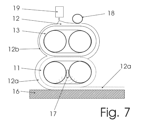
A device for carrying out the method according to the invention in another
5 embodiment is shown in Fig. 7. This is a transfer process in which the stamp
11
and the carrier 13 are configured as a continuous conveyor belt respectively
guided on and running around a roll pair. The flowable resist 12 is applied to
the
carrier conveyor belt 13 by means of a dispensing device 19 and the resist
coating of the carrier 13 set to a constant thickness by means of an evener
roll
10 18. On the opposite side of the carrier conveyor belt 13, the resist
coating 12 is
embossed by a stamp 11 which is configured as a conveyor belt and has an
outlined patterned surface. In the run-out of the contact or embossing portion
of
the two conveyor belts, the resist coating 12 continues to adhere only
partially
on the stamp conveyor belt 11. A second part 12b is entrained with the carrier
conveyor belt 13. In a contact portion of the conveyor belt, a first part 12a
with
the surface embossed by the patterned surface of the stamp 11 is transferred
to
a surface of the substrate 16 which is moved parallel to the stamp conveyor
belt
11. At the same time, the resist coating is cured by means of UV irradiation
by a
UV lamp 17. For this purpose, the material of stamp conveyor belt 11 is made
from flexible polymer material transparent to UV radiation. After curing, the
first
part 12a of the patterned resist coating adheres to the substrate 16 and the
demolding of the stamp conveyor belt 11 in its run-out area takes place. The
method according to the invention can be carried out continuously with the
above-described device.