Note: Descriptions are shown in the official language in which they were submitted.
CA 02735202 2010-09-10
20104. 80 19440 NO. 7O7 P. 4
DESCRIPTION
WAFER BONDING APPARATUS
Technical Field
The present invention is related to a wafer
bonding apparatus, and more particularly to a wafer
bonding apparatus configured to perform pressure
bonding on two substrates.
=
Background Art
A HEMS device is known in which minute
electrical parts and machine parts are integrated. As
such a HEMS device, a micro-relay, a pressure sensor,
in acceleration sensor and so on are exemplified. The
MEMS device is desired to have a high bonding strength
and to be manufactured by using a room-temperature
bonding technique which does not need a pressing
process due to load and a heating process.
A wafer bonding method is also known in which
a plurality of devices are formed on a bonding
. substrate obtained by bonding two substrates with a
plurality of patterns. In the method, it is desired
to improve a yield of the plurality of devices and to
apply a load on the bonding plane more uniformly.
In Japanese Patent Publication (JP-A-Heisei
09-321097), a pressing apparatus is disclosed in which
CA 02735202 2013-09-04
52313-7
- 2 -
even when contact surfaces of bumps on a work with the bumps
are inclined, all the bumps can be pressed against an electrode
of a work with uniform force. The pressing apparatus of the
work with bumps includes a pressing body driven by a driving
unit to move up and down, and an elastic member attached to the
lower surface of the pressing body and pressed to the upper
surface of the work, with bumps. A concave portion is formed in
the lower surface of the pressing body in order to permit that
the elastic member is expanded into an upper direction to
elastically deform.
In Japanese Patent Publication (JP 2007-301593A), a
pressing apparatus is disclosed in which uniform pressure can
be applied on a pre'ssure surface of a pressure object. In the
pressing apparatus, the pressure is applied to the pressure
object by a pressure head. The pressure head has a first space
section on a pressure axis of a pressing section.
Disclosure of the Invention
According to an aspect of the present invention,
there is provided a wafer bonding apparatus comprising: a first
sample base provided in a bonding chamber and configured to
hold a first substrate; a second sample base provided in said
bonding chamber and configured to hold a second substrate to
oppose to said first substrate; a load transferring section
coupled to an outer edge portion of said first sample base and
configured to support said first sample base to a first stage,
wherein said load transferring section is provided in said
bonding chamber; an angle adjusting mechanism provided in said
bonding chamber and configured to support said first sample
CA 02735202 2013-09-04
52313-7
base to said first stage through said load transferring section
such that an orientation of said first sample base is
changeable; and a drive unit configured to perform pressure
bonding on said first substrate and said second substrate by
driving said first stage to said second sample base.
Some embodiments of the present disclosure may
provide a wafer bonding apparatus in which a load is uniformly
applied to bonding surfaces of substrates.
A wafer bonding apparatus of an aspect of the present
invention includes a first sample base configured to hold a
first substrate; a second sample base
=
CA 02735202 2013-09-04
52313-7
= - 3 -
configured to hold a second substrate to oppose to the
first substrate; a load transferring section coupled
to an outer edge portion of the first sample base and
=
configured to support the first sample base to a first
stage; and a drive unit configured to perform pressure
bonding on the first substrate and the second
substrate by driving the second sample base to the
first stage. In the wafer bonding apparatus, it is
possible to prevent that a load which is larger than a
load applied on the outer edge portion of the first
substrate is applied to the center of the first
substrate, and to apply uniform load to the first
substrate and the second substrate, when pressure
bonding is performed on the first substrate and the
second substrate.
The wafer bonding apparatus according to the
present invention further includes an angle adjusting
mechanism configured to support a first sample base to
a first stage through the load transferring section.
That is, the load transferring section is preferable
for the wafer bonding apparatus which includes such an
angle adjusting mechanism.
The angle adjusting mechanism includes a
spherical flange fixed on the first sample base; a
spherical base fixed on the first stage; and a
fixation flange configured to fix the sphere flange on
= the sphere base by swaging the sphere flange. That
CA 02735202 2010-09-10
20104 911 88 19I46i NO. 77O P. 7
- 4 -
is, the load transferring section is preferable for
the wafer bonding apparatus which includes such a
spherical flange, spherical base and fixation flange.
The angle adjusting mechanism is in line-
contact with the load transferring section such that
the load transferring section is supported by the
.angle adjusting mechanism. At this time, the load
transferring section is preferable in that the
movement from the angle adjusting mechanism to a
position to which load is applied is very less.
The load transferring section includes a
plurality of columnar members, each of which is
coupled at one end to the outer edge portion of the
first sample base and at the other end to the angle
adjusting mechanism.
The load transferring section includes a
plurality of columnar members, which deform
elastically such that the first substrate and the
second substrate fit to each other when the pressure
bonding of the first substrate and the second
substrate is performed.
=
Brief Description of Drawing
FIG. 1 is a sectional view showing a wafer
bonding apparatus according to the present invention;
FIG. 2 is a sectional view showing the wafer
bonding apparatus;
CA 02735202 2010-09-10
2014 9fl 88 19447 NO. ]7U P. 8
- 5 -
FIG. 3 is a sectional view showing an angle
adjusting mechanism, a load transferring section and a
lower sample base;
FIG. 4 is a perspective view showing the load
transferring section;
FIG. 5 is a sectional view showing another
load transferring section;
FIG. 6 is a sectional view showing still
another load transferring section; .
FIG. 7 is a sectional view showing yet still
another load transferring section; and
FIG. 8 is a perspective view showing another
angle adjusting mechanism.
Best Mode for Carrying Our the Invention
Referring to the attached drawings, a wafer
bonding apparatus according to an embodiment of the =
present invention will be described in detail. The
wafer bonding apparatus 1 includes a bonding chamber 2
and a load lock chamber 3, as shown in FIG. 1. The
bonding chamber 2 and the load lock chamber 3 are
formed as containers in which the internal spaces are
shielded from external environment. Moreover, the
wafer bonding apparatus 1 includes a gate valve 5.
The gate valve 5 is interposed between the bonding
chamber 2 and the load lock chamber 3 and is operated
to close and open a gate which connects the internal
CA 02735202 2010-09-10
2014 911 80 19447S} NO. 7O7 P. 9
- 6 -
=
space of the bonding chamber 2 and the internal space
of the load lock chamber 3.
. The load lock chamber .3 includes an upper
cartridge base 6, a lower cartridge base 7, and a
conveyer unit 8 in the internal space. An upper
cartridge 11 is provided on the upper cartridge base
6, and a lower cartridge 12 is provided on the lower
cartridge base 7. Moreover, the load lock chamber 3
includes a vacuum pump and a lid, which are not shown,
The vacuum pump evacuates the internal space of the
load lock chamber 3. As the vacuum pump, a turbo-
molecular pump is exemplified which exhausts by
flicking gaseous molecules by a plurality of metal
wings. The lid closes the gate which connects the.
inside and outside of the load lock chamber 3 so that
the internal space of the chamber 3 is set to
atmosphere. The inner size of the gate is larger than
the outer sizes of. the upper cartridge 11 and lower
cartridge 12.
The conveyer unit 8 conveys the upper
cartridge 11 and the lower cartridge 12 from the load
lock chamber 3 to the bonding chamber 2 through the -
gate valve 5, and conveys the upper cartridge 11 and
the lower cartridge 12 from the bonding chamber 2 to
the load lock chamber 3 through the gate valve 5.
The bonding chamber 2 includes a vacuum pump
31, an ion gun 32 and an electron gun 33. In the
CA 02735202 2010-09-10
2014 9A 8B 194473 NO. 7070 P. 10
- 7 -
bonding chamber 2, an exhaust vent 35 is formed in a
part of a wall 34 of the chamber 2. The vacuum pump
31 is arranged outside the bonding chamber 2 and
exhausts gas through the exhaust vent 35 from the
internal space of the bonding chamber 2. As the
vacuum pump 31, a turbo-molecular pump is exemplified
which exhausts gas by flicking gaseous molecules by
plurality of metal wings. The ion gun 32 is arranged
to be directed to one irradiation direction 36 and
irradiates accelerated charged particles into the
irradiation direction 36. As the charged particles,
argon ions are exemplified. Another surface cleaning
unit. may be used to clean up the surface of a wafer in
place of the ion gun 32. As the other surface
'cleaning unit, a plasma gun, a high-speed atom beam
source and so on are exemplified. The electron gun 33
is arranged to be directed to an object to which the
charged particles are irradiated from the ion gun 32,
and irradiates accelerated electrons to the object.
The wall 34 is provided with a door 37 which
=
is formed in a part of the wall_ The door 37 is
provided with a hinge 38. The hinge 38 turnably
supports the door 37 to the wall 34. Moreover, the =
door 34 is provided a window 39 formed in a part of
the door. The window 39 is formed of material which
transmits light without transmitting gas. The window
39 may be arranged at anywhere of the wall 34 if a
CA 02735202 2010-09-10
2014 9)1 80 19447i1 NO.7070 P. 11
=
- 8 -
user can see the object to which the charged particles
are irradiated from the ion gun 32 or a bonding state
of the object from outside the bonding chamber 2.
As shown in FIG. 2, the bonding chamber 2'
further includes an upper substrate supporting section
41 and a lower substrate supporting section 42. The
lower substrate supporting section 42 is arranged in a
lower portion of the bonding chamber 2. The upper .
substrate supporting section 41 includes an upper
stage 14, an angle adjusting mechanism 15, a load
transferring section 16, an upper sample base 17 and a
pressure bonding mechanism 18. The upper stage 14 is
supported movably in a vertical direction to the
bonding chamber 2. The angle adjusting mechanism 15
supports the load transferring section 16 to the upper
stage 14. The load transferring section 16 supports
the upper sample base 17 to the angle adjusting
mechanism 15. The upper sample base 17 includes a
dielectric layer in the lower tip, applies voltage
between the dielectric layer and the substrate or
wafer to adhere the substrate or wafer to the
dielectric layer with electrostatic force. The
pressure bonding mechanism 18 moves the upper stage 14
in the vertical direction to the bonding chamber 2 in
accordance with an operation of the user.
The ion gun 32 is directed to the inner
surface of a portion of the wall 34 of the bonding
CA 02735202 2010-09-10
2010* 911 BB 19'47 S NO. 7070 P. 12
- 9 -
chamber 2 and a space between the substrate supported
= by the upper substrate supporting section 41 and the
substrate supported by a lower substrate supporting
section 42 when the substrate supported by the upper
substrate supporting section 41 and the substrate
supported by the lower substrate supporting section 42
are separated from each other. That is, the
irradiation direction 36 of the ion gun 32 passes
through the space between the substrate supported by
the upper substrate supporting section 41 and the
substrate supported by the lower substrate supporting
section 42, and intersects the inner surface of the
portion of the wall 34 of the bonding chamber 2.
As shown in FIG. 3, the lower substrate
supporting section 42 includes a lower sample base 46.
The lower sample base 46 is formed in the form of a
disk. In the lower sample base 46, a flat support
plane is formed on the upper surface of a circular
column. The lower sample base 46 is used to hold a
lower wafer 62 from the lower cartridge 12. Moreover, .
the lower substrate supporting section 42 includes an
alignment unit and a positioning mechanism (which are
not shown). The alignment unit picks up an image of
an alignment mark formed on the wafer or substrate
which is held by the lower sample base 46, in
accordance with an operation of the user. Moreover,
the alignment unit picks up an image of an alignment
CA 02735202 2010-09-10
2010if 9f1 BB 19114Th NO. 7070 P. 13
- 10 -
mark formed on the wafer which is held by the upper
sample base 17, in accordance with an operation of the
user, when the upper sample base 17 becomes close to
the lower sample base 46. The positioning mechanism
moves the lower sample base 46 in a horizontal
direction to the bonding chamber 2 and rotates the
lower sample base 46 around a rotation axis parallel
to the vertical direction.
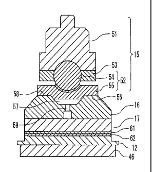
As shown in FIG. 3, the angle adjusting
mechanism 15 includes a spherical base 51, a spherical
flange 52 and a fixation flange 53. The spherical
base 51 is fixed on the upper stage 14 to form a
spherical base surface. The spherical flange 52 is
formed from a flange section 54 and a supporting
section 55. The flange section 54 is formed in a
spherical shape to fit to the spherical base surface
of spherical base 51. The supporting section 55 is
formed in a disk shape. The supporting section 55 is
in contact with the flange section 54 in the center of
the disk and a support surface 56 is formed on a back
face 56 of the supporting section 55 opposing to the
surface contacting the flange section 54. The
fixation flange 53 is coupled with the flange section
54 of spherical flange 52 by the swaging fixation.
That is, the fixation flange 53 is formed from split
ring portions. The split ring portions are arranged
to put the flange section 54 of the spherical flange
CA 02735202 2010-09-10
2014 911 80 19447i NO. 7070 P. 14
- 11 -
52 between the split ring portions, and couple to each
other by bolts (not shown), in order to couple the
fixation flange 53 to flange section 54 of the
spherical flange 52. Moreover, the fixation flange 53
is coupled to the spherical base 51 by coupling member
such as bolts so that the spherical base surface of
the spherical base 51 fits with the flange section 54
of spherical flange 52.
As shown in FIG. 4, the load transferring
section 16 is formed in the form of a disk. The load
.transferring section 16 has a concave section in the
center portion and a support surface 58 is formed on
the upper surface. The support surface 58 is flat and
is formed to be surrounded by two concentric circles.
The load transferring section 16 has a bolt hole 59 at
the center of the disk. In the load transferring
section 16, the bolt (not shown) is inserted in the
bolt hole 59 and is screwed with the supporting
section 55 of the spherical flange 52 as shown in FIG.
3. In this way, the load transferring section 16 is
supported to the spherical flange 52 such that the
support surface 58 is fit to the support surface 56,
and a cavity 57 is formed at the center of the load =
transferring section 16 attached to the supporting
5 section 55 of the spherical flange 52.
Moreover, the upper sample base 17 is coupled
to the back surface of the load transferring section
CA 02735202 2010-09-10
20104 911 BB 191i473) NO. 7070 P. 15
- 12 -
16 opposing to the support surface 58. The upper
sample base 17 is formed in the shape of a disk and
the upper sample base 17 includes the dielectric, layer
on the back surface opposing to the surface coupled to
the load transferring section 16. The upper sample
base 17 attaches the upper wafer 61 to the dielectric
layer with the electrostatic force by applying a
voltage to the dielectric layer.
= In an operation of bonding wafers by using
the wafer bonding apparatus 1, an operator first'
measures an orientation of the upper sample base 17.
The operator adjusts an angle by using the angle
adjusting mechanism 15 so that the surface of the
upper sample base 17 and the surface of the lower
sample base 46 are in parallel to each other, when the
surface of the upper sample base 17 for the upper
wafer 61 and the surface of the lower sample base 46
for the lower wafer 62 are not parallel to each other.
That is, the operator performs the swaging fixtation
of the spherical flange 52 to the fixation flange 53
and fixes the fixation flange 53 to the spherical base
51 so as to keep the surface of the upper sample base
= 17¨and the surface of the lower sample base 46
parallel.
Next, the operator closes the gate valve 5,
generates a vacuum atmosphere inside the bonding
chamber 2 by using the vacuum pump 31, and generates
CA 02735202 2010-09-10
2014 9f1 80 19447S1 NO. 77U P. 16
- 13 -
an ordinary pressure atmosphere inside the load lock
chamber 3. The operator opens the lid of the load
lock chamber 3 and arranges the upper cartridge 11 on
the upper cartridge base 6 and arranges the lower
cartridge 12 on the lower cartridge base 7. Then, the
operator puts the upper wafer 61 on the upper
cartridge 11, and puts the lower wafer 62 on the lower
cartridge 12. Next, the operator closes the lid of
the load lock chamber 3, and generates a vacuum
atmosphere inside the load lock chamber 3.
After the vacuum atmosphere is generated
inside the load lock chamber 3, the operator opens the
gate valve 5. At first, the operator sets the upper
wafer 61 on the upper sample base 17. The operator
conveys the upper cartridge 11 mounted with the upper
wafer 61 to the lower sample base 46 by the conveyer
unit B to hold the upper cartridge 11. The operator
accommodates the conveyer unit B inside the load lock
chamber 3. Next, the operator operates to lower the
upper sample base 17 in the vertical direction, to
make the dielectric layer of the upper sample base 17
contact the upper wafer 61, and to hold the upper
wafer 61 by the upper sample base 17. The operator
operates to raise the upper sample base 17 in the up
direction so as to separate the upper wafer 61 from
the upper cartridge 11. After the upper wafer 61 is
removed from the upper cartridge 11, the operator
CA 02735202 2010-09-10
2014 9)1 88 194483 " = NO. 7070 P. 17
- 14 -
conveys the upper cartridge 11 on which there is not
the upper wafer 61, from the lower sample base 46 to
the upper cartridge base 6 by the conveyer unit 8.
After the upper wafer 61 is set to the upper sample
base 17, the operator conveys the lower cartridge 12
mounted with the lower wafer 62 to the lower sample
base 46 by the conveyer unit 8 to hold the lower
cartridge 12.
The operator closes the gate valve 5, and
performs the pressure bonding of the upper wafer 61
held by the upper sample base 17 and the lower wafer
62 held by the lower sample base 46. That is, the
operator operates the ion gun 32 to irradiate charged
particles into a space between the upper wafer 61 and
the lower wafer 62 in the state that the upper wafer
61 held by the upper sample base 17 and the lower
wafer 62 held by the lower sample base 46 are
separated from each other. The charged particles are
irradiated into the space between the upper wafer 61
and the lower wafer 62 to remove oxide films formed in
the surfaces of the wafers and so on, and to remove
= impurities adhered to the surfaces thereof. The
operator operates the pressure bonding mechanism 18 to
lower the upper sample base 17 in the down direction
and to approach the upper wafer 61 to the lower wafer
62. The operator adjusts the position of the lower
wafer 62 held on the lower sample base 46 by the
CA 02735202 2010-09-10.
2010* 9f1 88 19048S) NO. 7070 P. 18
- 15 -
positioning mechanism such that the upper wafer 61 and
the lower wafer 62 are bonded in accordance with a
design. The operator operates the pressure bonding
mechanism 18 for the upper sample base 17 to lower the
upper sample base 17 in the down direction to perform
the pressure bonding of the upper wafer 61 the lower
wafer 62. The upper wafer 61 and the lower wafer 62
are bonded through the pressure bonding and one bonded
substrate is produced.
After the bonded substrate is dechucked from
the upper sample base 17, the operator operates to
raise the upper sample base 17 in the up direction.
Next, the operator opens the gate valve 5, and conveys
the lower cartridge 12, on which the bonded substrate
is put, from the lower sample base 46 to the lower
cartridge base 7 by the conveyer unit 8. The operator
closes the gate valve 5 and returns the inside space
of the load lock chamber 3 to the ordinary pressure
atmosphere. The operator opens the lid of the load .
lock chamber 3 and takes out the bonded substrate from
the lower cartridge 12 arranged on the lower cartridge
base 7.
In other conventional wafer bonding
apparatuses in which upper sample base is directly
fixed on an angle adjusting mechanism, the upper
sample base deforms elastically in case of the
pressure bonding such that the center portion of the'
CA 02735202 2010-09-10
2014 911 80 1904H NO. 7070 P. 19
- 16 -
upper sample base projects toward the lower sample
base. At this time, there is a case that uniform load
cannot be applied on the bonded surfaces of the upper
wafer 61 and the lower wafer 62, because larger load
is applied to the center portions of the upper wafer
and the lower wafer than the outer edges of them. In
the wafer bonding apparatus 1 of the present
invention, uniform load can be applied onto the
bonding surfaces of the upper wafer 61 and the lower
wafer 62 in the pressure bonding of the upper wafer 61
and the lower wafer 62. As a result, in the wafer
bonding apparatus 1, the production yield of the
bonded substrate can be improved, and the reliability
of the room-temperature bonding can be improved for
practical use.
Another load transferring section may be used
to apply the load from the upper stage 14 on the outer
edge portion of the upper sample base 17 in place of
the load transferring section 16.
FIG. 5 shows another example of the load
transferring section. Like the load transferring
section 16, the load transferring section 65 is formed
in the shape of a disk. The load transferring section
65 has a concave portion formed at the center of the
upper portion and a support surface 66 is formed on
the upper portion. The support surface 66 has a
curved surface which represents a part of the surface
CA 02735202 2010-09-10
= 2014 9f1 8B 19*483}
No. 7070 P. 20
- 17 -
of a so-called doughnut shape formed by rotating an
ellipse around a rotation axis. The rotation axis
passes through the center of the disk of the load
transferring section 65 perpendicularly to the disk.
A bolt hole 67 is formed at the center of the disk of
the load transferring section 65. A bolt (not shown)
is inserted in the bolt hole 67 of the load
transferring section 65 and is fastened to the
supporting section 55 of the spherical flange 52.
Thus, the load transferring section 65 is supported to
the spherical flange 52 such that the support surface
= 66 makes line contact with the support surface 56 and
the cavity 57 is formed at the center, of the surface
portion of the load transferring section 65 with which
the supporting section 55 of the spherical flante 52
is in contact.
When the load applied from the upper stage 14
is small, the load transferring section 16 receives
the load with the whole support surface 66. When the
load applied from the upper stage 14 is large, the
supporting section 55 of the spherical flange 52
. deforms elastically and the load transferring section
16 receives the load with the edge of the support
surface 58 on the center side. In this way, a
position of the load transferring section 16 which
receives the applied load from the upper stage 14
. moves depending on the magnitude of the load applied
CA 02735202 2010-09-10
2010* 911 8B 19448i NO. 7070 P. 21
- 18 -
from the upper stage 14. Therefore, the wafer bonding
apparatus 1 has a possibility that the uniform load
cannot be applied on the bonding plane of the upper
wafer 61 and the lower wafer 62 when the load is
large.
The load transferring section 65 reduces the
movement of the position which receives the load
applied from the upper stage 14. As a result, the
water bonding apparatuses to which the load
transferring section 65 is applied can apply a uniform
load on the bonding surfaces of the upper wafer 61 and
the lower wafer 62 even when the magnitude of the load
applied from the upper stage 14 is changed.
FIG. 6 shows another example of the load
transferring section_ The load transferring section
71 is formed from a plurality of columnar members 72-1
to 72-n (n=3, 4, ...). The plurality of columnar
members 72-1 to 72-n are respectively arranged in a
plurality of positions obtained by equally dividing
the outer edge of the upper sample base 17. One end
of each 72-i (i=1, 2, 3, n) of the plurality of
columnar. members 72-1 to 72-n is fixed on the
supporting section 55 of the spherical flange 52 and
the other end is fixed on the outer edge of the upper
sample base 17.
In the wafer bonding apparatus to which such
a load transferring section 71 is applied, when the
CA 02735202 2010-09-10
2014 9f1 813 19448i NO. 77 P. 22
- 19 -
pressure bonding is performed on the upper wafer 61
and the lower wafer 62, the uniform load can be
applied on the bonding surfaces of the upper wafer 61
and the lower wafer 62, like the above wafer bonding
apparatus 1. Thus, the reliability of the bonding can
be improved.
= FIG. 7 shows another example of the load
transferring section. The load transferring section
92 is formed from a plurality of 'springs 93-1 to 93-n.
The plurality of springs 93-1 to 93-n are respectively
arranged in a plurality of regions obtained by equally
dividing the outer edge of the upper sample base 17
into n regions. Each 93-i of the plurality of springs
93-1 to 93-n is fixed on a supporting section 91 which
is fixed on the supporting section 55 of the spherical
flange 52 at one end and fixed on the outer edge of
the upper sample base 17 at the other end.
In the wafer bonding apparatus to which such
a load transferring section 92 is applied, like the
above wafer bonding apparatus 1, when the pressure
bonding is performed on the upper wafer 61 and the
lower wafer 62, a uniform load can be applied on the =
bonding surfaces of the upper wafer 61 and the lower
wafer 62. Thus, the reliability of the bonding can be
improved. Also, in the wafer bonding apparatus to
which such a load transferring section 92 is applied,
when the upper wafer 61 and the lower wafer 62 are not
=
CA 02735202 2010-09-10
2014 911 88 19448i NO. 7070 P. 23
.
- 20 -
in parallel to each other, the plurality of springs
93-1 to 93-n deform elastically such that the upper
wafer 61 and the lower wafer 62 become parallel to
each other in the pressure bonding. Therefore, in
such a wafer bonding apparatus, even when the upper
wafer 61 and the lower wafer 62 are not parallel to
each other, the uniform load is applied to the bonding
surfaces of the upper wafer 61 and the lower wafer 62
in the pressure bonding. As a result, in such a wafer
bonding apparatus, it is not necessary =to adjust the
hold surface of the upper sample base 17 and the hold
surface of the lower sample base 46 by. the angle
adjusting mechanism 15 before the pressure bonding,
= and the pressure bonding can be more easily performed
on the upper wafer 61 and the lower wafer 62..
Moreover, the angle adjusting mechanism 15 can be
omitted and such a wafer bonding apparatus can be
cheaply manufactured.
Another angle adjusting mechanism may be used
to fix the direction of the upper sample base 17 on a
predetermined direction in place of the angle
adjusting mechanism 15.
FIG. 8 shows an example of another angle
adjusting mechanism. The angle adjusting mechanism 81
includes a first frame 82, an intermediate body 83, a
second frame 84 and a supporting section 85. The
first frame 82 is fixed on the upper stage 14. The
CA 02735202 2010-09-10
2010* 9A 88 19483 NO. 7070 P. 24
- 21 -
intermediate body 83 is supported by the first frame
82 with a bolt 86 rotatably around a rotation axis 88.
The rotation axis 88 extends in parallel to a
horizontal direction and is fixed to the first frame
82. The bolt 86 is fastened to the intermediate body
83 to fix the intermediate body 83 on the first frame
= 82. The second frame 84 is supported by the
intermediate body 83 with a bolt 87 rotatably around a
rotation axis 89. The rotation axis 89 extends in
parallel to the horizontal direction and is
perpendicular to the rotation axis 88 and is fixed to
the intermediate body 83. The bolt 86 is fastened to
the intermediate body 83 to fix the first frame 82 on
the intermediate body 83. The supporting section 85
is formed in the shape of a disk and the center of the
disk is fixed on the second frame 84. Moreover, in
the supporting section 85, a flat support surface is
formed on the back surface opposing to the surface
bonded with the second frame 84. Like the above angle
adjusting mechanism 15, the angle adjusting mechanism
81 supports the load transferring section 16 such that
= the support surface of the supporting section 85 fits
to the support surface 58 of the load transferring
section 16 and that the cavity 57 is formed in the
load transferring section 16.
The wafer bonding apparatus to which the
angle adjusting mechanism 81 is applied can apply a
=
CA 02735202 2010-09-10
2014 9)1 88 194483) NO. 7070 P. 25
- 22 -
uniform load on the bonding surfaces of the upper
wafer 61 and the lower wafer 62 when the pressure
bonding is performed on the upper wafer 61 and the
lower wafer 62, like the wafer bonding apparatus 1.
Thus, the reliability of the bonding can be improved.
The wafer bonding apparatus of the present
invention can prevents that a load larger than load
applied on the outer edge of the first substrate is
applied at the center of the first substrate when the
first substrate and the second substrate are subjected
to the pressure bonding, and the load can be uniformly
applied on the first substrate and the second
substrate.
=