Note: Descriptions are shown in the official language in which they were submitted.
CA 02735666 2011-02-28
WO 2010/033668 PCT/US2009/057264
ANALYTE SENSORS, TESTING APPARATUS AND MANUFACTURING METHODS
RELATED APPLICATIONS
The present application claims priority to U.S.
Provisional Patent Application No. 61/098,720 filed
September 19, 2008, and entitled "ANALYTE SENSORS AND
MANUFACTURING METHODS" (Attorney Docket No. BHDD-003/L)
which is hereby incorporated herein by reference in its
entirety for all purposes.
FIELD OF THE INVENTION
The present invention relates to electrochemical
analyte sensors that may be used to detect an analyte
concentration level in a bio-fluid sample, apparatus
including the analyte sensors, and methods of manufacturing
thereof.
BACKGROUND OF THE INVENTION
The monitoring of analyte concentration levels in a
bio-fluid may be an important part of health diagnostics.
For example, an electrochemical analyte sensor may be
employed for the monitoring of a patient's blood glucose
level as part of diabetes treatment and care.
An electrochemical analyte sensor may be employed
discretely ('discrete monitoring'), for instance, by
detecting an analyte concentration level in bio-fluid sample
such as from a single sample of blood or other interstitial
fluid obtained from the patient via a lancet (e.g., by a
pin-prick or needle). Optionally, the analyte sensor may be
employed continuously ('continuous monitoring'), by
implanting the sensor in the patient for a duration of time.
In discrete monitoring, there may be a separation between
1
CA 02735666 2011-02-28
WO 2010/033668 PCT/US2009/057264
the bio-fluid sample collection process and the measurement
of the analyte concentration level. Typically, after a bio-
fluid sample has been obtained from the patient, such as by
the use of a lancet, the sample may then be transferred to a
medium (e.g., a test strip sensor or a detector) for
measurement of the bio-fluid sample's analyte concentration
level.
Because conventional electrochemical analyte sensors
may have relatively low sensitivity and because transfer of
the bio-fluid sample to the sensor may be relatively
inefficient, a relatively large sample volume may be
required in order to yield an accurate measurement of the
analyte concentration level. In such instances, if the
provided sample has an insufficient sample volume, then
either no reading or an inaccurate reading may result.
Accordingly, an additional bio-fluid sample may need to be
drawn and, consequently, lancet insertion may need to be
repeated which may cause further pain and discomfort to the
patient.
Additionally, conventional sensors may require the use
of precious metals for the working and/or reference/counter
electrodes which may add significantly to the cost of the
analyte sensors.
It may, therefore, be beneficial to provide an analyte
sensor adapted for bio-fluid analyte sampling that may
consistently provide for analyte concentration level
measurements from an obtained bio-fluid sample, which may
require a lessened sample volume, and/or which may also
provide for lower cost manufacture.
2
CA 02735666 2011-02-28
WO 2010/033668 PCT/US2009/057264
SUMMARY OF THE INVENTION
In a first aspect, the present invention provides an
analyte sensor including a base; a first sensor member
coupled to the base, the first sensor member comprising a
semiconductor material; a second sensor member coupled to
the base and spaced from the first sensor member; and an
active region in contact with at least the first sensor
member.
In another aspect, the present invention provides an
analyte sensor for detecting an analyte concentration level
in a bio-fluid sample, including a base; a first sensor
member coupled to the base and comprised of a semiconductor
material; a cavity formed proximate to an end of the first
sensor member; and an active region positioned within the
cavity, the active region being coupled to an end of the
first sensor member.
In another aspect, the present invention provides an
analyte sensor for detecting an analyte concentration level
in a bio-fluid sample, including a base; a fiber sensor
member coupled to the base, the fiber sensor member
including at least a portion which is made of a
semiconductor material; a cavity formed proximate to an end
of the fiber sensor member; and an active region positioned
within the cavity, the active region being coupled to an end
of the fiber sensor member.
In yet another aspect, the present invention provides
an analyte sensor for detecting an analyte concentration
level in a bio-fluid sample, including an insulating base, a
first sensor member coupled to the base and comprised of a
core of conductive material and a cladding of a
semiconductor material surrounding the core, a second sensor
member coupled to the base and comprised of a core of
conductive material and a cladding of a semiconductor
3
CA 02735666 2011-02-28
WO 2010/033668 PCT/US2009/057264
material surrounding the core, a cavity formed proximate to
ends of the first and second sensor members, an active
region positioned within the cavity, the active region being
coupled to both the first and second sensor members, and a
lid attached to the insulating base wherein the base and lid
at least partially defining the cavity.
In another aspect, the present invention provides a
testing apparatus, including a port receiving an analyte
sensor, wherein the analyte sensor further comprises a base;
a first sensor member coupled to the base, the first sensor
member comprising a semiconductor material; a second sensor
member coupled to the base and spaced from the first sensor
member; and an active region in contact with at least the
first sensor member.
In a method aspect, the present invention provides a
method of manufacturing an analyte sensor including the
steps of providing a base; mounting a first sensor member on
the base wherein the first sensor member is comprised of a
semiconductor material; applying an active region on a
portion of the first sensor member; and providing a lid
coupled to the base.
In another method aspect, the present invention
provides a method of manufacturing analyte sensors,
including the steps of providing a sheet of base material;
mounting a plurality of fibers on the sheet of base material
wherein the fibers are comprised of a semiconductor
material; applying an active region on at least some of the
fibers; attaching lidstock to form a unitary body; and
cutting the unitary body to provide a plurality of analyte
sensors.
Other features and aspects of the present invention
will become more fully apparent from the following detailed
4
CA 02735666 2011-02-28
WO 2010/033668 PCT/US2009/057264
description, the appended claims and the accompanying
drawings.
BRIEF DESCRIPTION OF THE DRAWINGS
FIG. 1 is a top view of an exemplary embodiment of an
analyte sensor provided according to the present invention.
FIG. 2 is an enlarged cross-sectional view of the
analyte sensor of FIG. 1 taken along section line 2-2.
FIG. 3 is an exploded isometric view of the exemplary
embodiment of the analyte sensor of FIG. 1 according to the
present invention showing a lid being separated for clarity.
FIG. 4 is a frontal view of a testing apparatus
including an exemplary embodiment of an analyte sensor
received in a port of the apparatus according to the present
invention.
FIG. 5 is a top view of another exemplary embodiment of
an analyte sensor according to the present invention.
FIG. 6 is a partially cross-sectioned top view of
another exemplary embodiment of an analyte sensor according
to the present invention.
FIG. 7 is a top view of another exemplary embodiment of
an analyte sensor according to the present invention.
FIG. 8 is a enlarged partially cross-sectioned view of
a coded region of the analyte sensor embodiment of FIG. 7
according to the present invention.
FIG. 9 is a diagram illustrating a formation of
conductive tracks on a sensor member included within an
exemplary embodiment of an analyte sensor according to the
present invention.
FIG. 10A is a top view of another exemplary embodiment
of an analyte sensor according to the present invention.
5
CA 02735666 2011-02-28
WO 2010/033668 PCT/US2009/057264
FIG. 10B is a cross-sectioned side view of the
exemplary embodiment of FIG. 10A taken along section line
lOB-10B.
FIG. 11 is a flowchart illustrating methods of
manufacturing the analyte sensor members according to the
present invention.
FIG. 12 is a top view illustrating a plurality of the
analyte sensor members of FIG. 10A adapted to be cut from a
larger unitary body.
FIG. 13 is another flowchart illustrating methods of
manufacturing a plurality of the analyte sensors according
to the present invention.
DETAILED DESCRIPTION
According to an aspect of the present invention, an
analyte sensor is provided that includes a first sensor
member, such as a fiber comprised of a semiconductor
material (e.g., silicon carbide (SiC)). The first sensor
member may be mounted on a base (e.g., of an insulating
material). In some embodiments, the first sensor member may
include a conductive core which may comprise a part of a
working electrode of the analyte sensor and a cladding
comprised of the semiconductor material. An active region
may be provided in contact with at least the first sensor
member. For example, the active region may be in contact
with, and electrically coupled to, the first sensor member
such that analyte detection may be accomplished by
connection to a testing apparatus. A second sensor member
may also be mounted on the base, wherein the second sensor
may operate as a reference or counter electrode. The second
sensor member may also include a semiconductor material, and
in some embodiments, may be comprised of a conductive core
6
CA 02735666 2011-02-28
WO 2010/033668 PCT/US2009/057264
and a cladding comprised of a semiconductor material.
Similarly, the second sensor member may be in contact with,
and electrically coupled to, the active region. In some
embodiments, the conductive core of the first sensor member
and even the second sensor member may comprise carbon (e.g.,
graphite) and the cladding may comprise silicon carbide.
Additionally, the analyte sensor may include a cavity,
which may be located proximate to an end of the first sensor
member and the active region. The cavity may be adapted for
accepting a bio-fluid sample. The term "cavity" as defined
herein is a hollow, indented, or concave area having walls
adapted to contain and confine the bio-fluid sample. In
some embodiments, the cavity may be at least partially
formed and defined by the base and a lid, which is coupled
to the base.
The active region of the analyte sensor may include one
or more catalytic agents and/or reagents adapted to react
and convert an analyte in the bio-fluid sample received in
the cavity into reaction products from which an electrical
current may be generated. The resulting electrical current
may flow in the first sensor member (e.g., in the core
and/or cladding). The first sensor member, in some
embodiments, forms at least a portion of a working electrode.
The generated electrical current may then be detected, such
as by testing apparatus (e.g., an ammeter) connected to the
working electrode, thereby enabling a determination and
readout of an analyte concentration level contained in the
bio-fluid sample. The electrical current provided may have
a magnitude correlated with the concentration of the analyte
in the sample, for example.
These and other embodiments of analyte sensors,
apparatus including the analyte sensors and methods for
7
CA 02735666 2011-02-28
WO 2010/033668 PCT/US2009/057264
manufacturing the anaiyte sensors are described below with
reference to FIGs. 1-13.
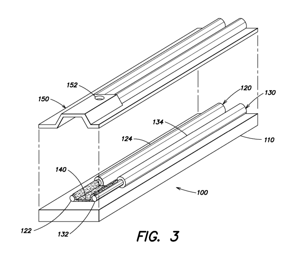
FIGs. 1-3 show various views of a first exemplary
embodiment of an analyte sensor 100 provided according to
the present invention. The analyte sensor 100 may include a
base 110 preferably formed of an insulating material. The
base 110 may have a first sensor member 120 mounted thereon.
The base 110 may be manufactured from of a polymer material,
such as a polycarbonate, polyethylene terephthalate,
polyimide, high-density polyethylene, or polystyrene
material, for example. Further, the first sensor member 120
may be mounted on the base 110 by including some level of
physical impression into the base 110. For example, when
the base 110 is a deformable polymer, sufficient pressure
and/or heat may be applied thereby causing the first sensor
member 120 to form an impression in the base 110.
Optionally, the impression may be molded into the base 110.
Optionally, the first sensor member 120 may be adhered,
glued, heat fused, ultrasonically fused, or otherwise
mounted to the base 110. In some embodiments, the first
sensor member 120 may be mounted to the base 110 simply by
sandwiching between the base 110 and a lid 150. The size
and shape of the base 110 is not of consequence and any
suitable size and shape may be used. The base 110 simply
functions as a way of mounting the sensor member 120 and to
allow ease of handling by the user.
The first sensor member 120 may include a semiconductor
material. For example, the sensor member 120 may include a
core 122 comprised of a conductive material and the cladding
124 which is comprised of a semiconductor material.
Preferably, the first member 120 is a fiber or filament with
a length much greater than its width. In some embodiments,
the fiber may include the conducting core 122, which may be
8
CA 02735666 2011-02-28
WO 2010/033668 PCT/US2009/057264
at least partially surrounded by the cladding 124. In the
exemplary embodiment shown, the cladding 124 may include an
annular shape, which may fully surround the core 122 along
at least a portion of the length of the core 122. The core
122 may comprise the shape of a cylindrical rod, for example.
Both the core 122, which may include the conductive material,
and the cladding 124, which may include the semiconductor
material, in operation may convey electrical current, albeit
the semiconductor material may include a much higher
resistivity as compared to the core 122 and, therefore, may
carry less current than the core 122. In some embodiments,
the core 122 may comprise carbon (e.g. graphite) and the
cladding 124 may comprise silicon carbide (SiC). SiC/C
fibers having a suitable SiC cladding and carbon core are
manufactured by Specialty Materials Inc. of Lowell,
Massachusetts, for example. However, the conductive
material of the core 122 may also comprise other
electrically conductive metal materials including the noble
metals (e.g., gold, silver, platinum, etc.), copper and
aluminum. The cladding 124 may comprise other semiconductor
materials including Group IV elements such as silicon and
germanium, Group IV compounds such as silicon germanide
(SiGe), and Group III-V compounds such as gallium arsenide
(GaAs) and indium phosphide (InP), among others. In some
embodiments, a semiconducting fiber with no conductive core
may be used.
In some embodiments, the first sensor member 120 may
have a total diameter (including the core 122 and cladding
124) of about 150 microns more less, about 100 microns or
less, about 75 microns or less, or even about 50 microns or
less, and between about 50 microns and about 150 microns in
some embodiments (although larger or smaller sizes also may
be used). The core 122 may have a diameter between about 10
9
CA 02735666 2011-02-28
WO 2010/033668 PCT/US2009/057264
to about 100 microns, or even between about 20 microns to
about 40 microns, and preferably about 30 microns, although
other dimensions may also be used. In the depicted
embodiment, the first sensor member 120 may include an end
portion where the core 122 is exposed (the 'stripped end').
This may enlarge and enhance the effective contact area, and
thus the conducting area, of the conductive core 122 such as
when the core 122 functions as an electrode. Any suitable
technique may be used to remove the cladding material
thereby forming the stripped end, such as machining, etching,
or the like. Electrochemical wet etching with an acid (e.g.,
HN, HCF or combinations) may be used. Other mechanisms for
enhancing the effective contact area of the core are
described below.
The analyte sensor 100 may further include a second
sensor member 130, which in some implementations may also
include a semiconductor material. The second sensor member
may include a core 132 comprised of a conductive material,
and a cladding 134 comprised of a semiconductor material,
for example. The materials for the second sensor member 130
may be the same as described above for the first sensor
member 120. Optionally, the second sensor member 130 may be
of more conventional materials, such as carbon, graphite,
gold, silver, palladium or platinum. For example, the
second sensor may be formed of a carbon/graphite PTF or
Ag/AgCl. Preferably, however, the second sensor member 130
may be, as shown in FIG. 1, another fiber, which may be
oriented in a generally parallel relationship to the first
sensor member 120, and may comprise a semiconductor material.
However, as is shown in FIG. 5, other orientations may be
provided, such as non-parallel.
Again referring to FIGs. 1-3, applied onto the base 110
and in contact with, and electrically coupled to, at least
CA 02735666 2011-02-28
WO 2010/033668 PCT/US2009/057264
the first sensor member 120 may be an active region 140
(which will be described more thoroughly below). Briefly,
however, the active region 140 may be adapted to be exposed
to the bio-fluid sample. The active region 140 may include
one or more catalytic agents or reagents adapted to promote
an electrochemical reaction between an analyte in the bio-
fluid sample and the catalytic agents or reagents included
in the active region 140. This produces reaction products
and mobile electrons, which then may be conducted, for
example, by the core 122 of the first sensor member 120. A
mediator, to be described later herein, may be provided in
the active region 140 to aid in carrying the electrons to
the surface of the conducting core 122.
According to some embodiments of the invention, a
cavity 155 may be formed and provided proximate to a working
end 135 of the first sensor member 120 having the exposed
core 122. The cavity 155 receives the bio-fluid sample
inserted through an open end, for example. In particular,
the cavity 155 may be at least partially formed and defined,
for example, by inner surfaces of the lid 150, and surfaces
of the base 110 (with active region 140 applied thereto).
The cavity 155 may have any shape, but preferably has a
shape, which promotes capillary action to cause a droplet of
bio-fluid to drawn in and come to rest between the
respective cores 122, 132 such that the sample is provided
in contact with the active region 140. A hole 152 may be
provided to assist capillary action of the bio-fluid. The
cavity 155 may have a length of about 2-5 mm and a width of
about 0.5 to 1.5 mm, for example.
In some embodiments, a sufficient bio-fluid sample for
purposes of detecting an analyte concentration level may
have a volume of less than about 0.5 microliters, less than
about 0.3 microliters, or even less than about 0.2
11
CA 02735666 2011-02-28
WO 2010/033668 PCT/US2009/057264
microliters, for example. Other sample volumes may also be
employed. Contributing to the need for a lessened volume of
the bio-fluid sample may be the use of the fiber-like shape
of the first sensor member 120. This may provide generally
opposed surfaces 141W, 141R (wherein the W stands for
"Working" and the R stands for "Reference") for the active
region 140 to be applied to, a three dimensional shape, as
well as a relatively large effective surface area of exposed
electrode. As such, excellent analyte detection may be
accomplished with a relatively small sample volume of the
bio-fluid. Accordingly, the propensity to have to prick the
finger, etc., a second time to obtain sufficient fluid
volume for testing may be minimized or avoided.
Referring to FIG. 2, the active region 140 may be
positioned within the cavity 155, and is preferably located
at a bottom of the cavity 155, thereby allowing exposure of
the active region 140 to the sample bio-fluid that enters
the cavity 155. As shown, the active region 140 is applied
over, and in contact with, the cores 122, 132. Upon
insertion of the bio-fluid sample into the cavity 155, an
electrochemical reaction takes place between the analyte in
the fluid sample and the catalytic agents or reagents of the
active region 140 to produce reaction products and generate
the flow of electrons. The core 122 may then conduct and
channel the electron flow and provide an electrical current,
which may be proportional to the concentration of the
analyte in the bio-fluid sample. This current may then be
conditioned and displayed in any suitable readout form, such
as in a digital readout 470 of a testing apparatus 460 (e.g.,
such as shown in FIG. 4).
As further shown in FIG. 4, an embodiment of an analyte
sensor 400 such as the analyte sensor described with
reference to FIGs. 1-3, or any of the additional embodiments
12
CA 02735666 2011-02-28
WO 2010/033668 PCT/US2009/057264
described herein, may be inserted and received into a port
465 of the testing apparatus 460. Electrical contacts (not
shown) in the apparatus 460 may come into electrical contact
with conductive ends of sensor members 120, 130 (e.g., the
cores and/or claddings thereof) thereby making an electrical
connection to the circuitry of the apparatus 460. Upon
applying a voltage bias (e.g., about 400 mV), conventional
processing programs and circuitry may then equate the
current supplied by the sensor member 120 to an analyte
concentration level.
Again referring to FIGs. 1-3, one group of catalytic
agents useful for providing the active region 140 may be the
class of oxidase enzymes which includes, for example,
glucose oxidase (which converts glucose), lactate oxidase
(which converts lactate), and D-aspartate oxidase (which
converts D-aspartate and D-glutamate). In embodiments in
which glucose is the analyte of interest, glucose
dehydrogenase (GDH) may optionally be used.
Pyrolloquinoline quinine (PQQ) or flavin adenine
dinucleotide (FAD) dependent may also be used. A more
detailed list of oxidase enzymes which may be employed in
the present invention is provided in U.S. Patent No.
4,721,677, entitled "Implantable Gas-containing Biosensor
and Method for Measuring an Analyte such as Glucose" to
Clark Jr. which is hereby incorporated by reference herein
in its entirety. Catalytic enzymes other than oxidase
enzymes may also be used.
The active region 140 may include one or more layers
(not explicitly shown) in which the catalytic agents (e.g.,
enzymes) and/or other reagents may be immobilized or
deposited. The one or more layers may comprise various
polymers, for example, including silicone-based or organic
polymers such as polyvinylpyrrolidone, polyvinyl alcohol,
13
CA 02735666 2011-02-28
WO 2010/033668 PCT/US2009/057264
polyethylene oxide, cellulosic polymers such as
hydroxyethylcellulose or carboxymethyl cellulose,
polyethylenes, polyurethanes, polypropylenes,
polyterafluoroethylenes, block co-polymers, sol-gels, etc.
A number of different techniques may be used to immobilize
the enzymes in the one or more layers in the active region
140 including, but not limited to, coupling the enzymes to
the lattice of a polymer matrix such as a sol gel, cross-
linking the agents to a suitable matrix such as
glutaraldehyde, electropolymerization, and formation of an
array between the enzymes via covalent binding, or the like.
In some embodiments, an electrochemically active layer
(not explicitly shown) may be positioned adjacent to an
exposed end (e.g., the stripped portion) of the sensor
member. The electrochemically active layer may include, for
example, noble metals such as platinum, palladium, gold or
rhodium, or other suitable materials. In a glucose
detection embodiment, the active layer may undergo a redox
reaction with hydrogen peroxide when polarized appropriately.
The redox reaction causes an electrical current to be
generated by electron transfer that is proportional to the
concentration of the analyte that has been converted into
hydrogen peroxide. This current may be conducted and
conveyed from the electrochemically active layer through the
core 122 and/or cladding 124 to a testing apparatus as
previously described with reference to FIG. 4.
In some embodiments, a mediator may be within the
active region 140 to promote the conversion of the analyte
to detectable reaction products. Mediators comprise
substances that act as intermediaries between the catalytic
agent and the working electrode (e.g., the surface of the
exposed core, a surface area enhancement of the core, or an
electrochemically active layer applied to the core, etc.).
14
CA 02735666 2011-02-28
WO 2010/033668 PCT/US2009/057264
For example, a mediator may promote electron transfer
between the reaction center where catalytic breakdown of an
analyte takes place and the working electrode, and may
enhance electrochemical activity at the working electrode.
Suitable mediators may include one or more of the following:
metal complexes including ferrocene and its derivatives,
ferrocyanide, phenothiazine derivatives, osmium complexes,
quinines, phthalocyanines, organic dyes as well as other
substances. In some embodiments, the mediators may be
cross-linked along with catalytic agents directly to the
working electrode.
As described above, the analyte sensor 100 may also
include a second sensor member 130, which may function as a
reference electrode providing a return path for an
electrical current. In one or more embodiments, the second
sensor member 130 may function as a counter electrode. As
described further with reference to FIGs. 1-3 and 5-10B, the
reference electrode may be arranged, formed and/or
implemented in a number of different ways. In the
embodiment depicted in FIGs. 1-3, the sensor member 130 may
comprise a fiber mounted to the base 110 and may be
comprised of a semiconductor material. For example, the
sensor member 130 may include a conductive core 132 and may
comprise a semiconducting cladding 134. However, it should
be recognized that the reference electrode may take on other
forms (e.g., a coil, foil, strip, or film) and may be made
from other suitable materials, such as the materials
described above.
To form an electrochemical cell, the second sensor
member 130 may be coupled to the active region 140 in the
cavity 155. In particular, the active region 140 may be
applied to be in contact with and configured to extend
between the cores 122, 132. The active region 140 may
CA 02735666 2011-02-28
WO 2010/033668 PCT/US2009/057264
extend along the generally opposed surfaces 141W, 141R of
the cores 122, 132 as best shown in FIG. 2, such that a drop
of bio-fluid (depicted by dotted line 156) may be received
in a three-dimensional feature formed by the active region
140 as applied over the surfaces of the cores 122, 132 and
base 110.
FIG. 5 illustrates another embodiment of an analyte
sensor 500 of the invention. As in the previously described
embodiments, the first and second members 520, 530 may be
mounted on a base 510 (e.g., of an insulating material) and
an active region 540 may be applied to, preferably in
contact with, the respective cores 522, 532 of the members.
However, in this embodiment, the members may be oriented in
other than a generally parallel relationship (e.g., at an
angle R of greater than 0 degrees and less than or equal to
90 degrees). In other words, the spacing between the
terminal ends 523, 533 of sensor members 520, 530 at the
terminal end 536 may be greater than the spacing between the
sensor members 520, 530 positioned in contact with the
active region 540 at the working end 535. This
configuration allows the sensor members 520, 530 and cores
522, 532 to be positioned very close together proximate the
active region 540, but separates the terminal ends 523, 533
of the members 520, 532 for ease of electrical connection to
a testing apparatus (not shown). A hole 552, for example,
may allow venting for ease of insertion of the bio-fluid
sample into an end of the cavity (not explicitly shown)
which is formed by the cooperation of the lid 550 and the
base 510 in the vicinity of the active region 540.
Electrical connection with a testing apparatus may be made
through electrical contact with the terminal ends 523, 533
of the sensor members 520, 530.
16
CA 02735666 2011-02-28
WO 2010/033668 PCT/US2009/057264
In order to enhance the effective conductive area of
the conductive core 122 of the first member 120 in the
embodiments shown in FIGs. 1-3 and FIG. 5, the cladding may
be stripped off along a length of the fiber. Additionally
or optionally, the inventors have discovered other
mechanisms, which may be used for enhancing the effective
conductive area of the working electrode in embodiments of
the invention.
In FIG. 6, for example, a partially sectioned top view
of another embodiment of an analyte sensor 600 is
illustrated. In the embodiment depicted in FIG. 6, first
and second sensor members 620, 630 may be mounted to a base
610 as in the previous embodiments. However, in this
embodiment, an effective conductive area of the electrode
may be increased by providing a conductive coating 680W on
an end of the core 622. Similarly, the second sensor member
630 may include a coating 680R.
In this depicted embodiment, the active region 640 may
be provided on the base 610 and in contact with the
generally opposed surfaces 641W, 641R of the sensor members
620, 630. The coatings 680R, 680W may comprise carbon or
any other suitable conductive material (e.g., Ag/AgCl, gold,
silver, palladium, copper, aluminum, etc). In the present
embodiment, the coatings 680W, 680R may be provided in
electrical contact with simply cleaved ends of the cores 622,
632 and may be coated on the entire end of the members 620,
630, but may also be coated on peripheral surfaces of the
claddings 624, 634. As such, the effective conductive area
of the cores, which are exposed to the active region 640,
may be substantially increased, in that the conductive
coatings 680W, 680R function as extensions of the cores and
the surfaces of the coatings 680W, 680R may become the
working and reference electrodes, respectively. Accordingly,
17
CA 02735666 2011-02-28
WO 2010/033668 PCT/US2009/057264
the active region 640 may be placed in contact with the
cores 620, 630 over a relatively larger area. Optionally,
the effective contact area of the cores may be enhanced by
performing a cleave operation at the end of the members 120,
130 at other than a right angle (e.g., other than a simple
cleave) thereby exposing more of the core.
Additionally shown in this embodiment of FIG. 6 is
another method of providing an electrical contact between
the analyte sensor 600 and a testing apparatus (not shown).
In the previous embodiments, the electrical contact with the
testing apparatus was by way of electrical contact with the
terminal ends of the sensor members 120, 130 (FIGs. 1-3) and
520, 530 (FIG. 5). In contrast, the electrical contact in
the current embodiment to the working and reference
electrodes may be by contact with electrical contact patches
690W and 690R. The contact patches 690W, 690R are comprised
of a conductive binding compound such as a conductive epoxy
(e.g., silver epoxy or carbon epoxy) which is provided in
contact with the cores 622, 632 and/or claddings 624, 634 of
first and second sensor members 620, 630. As shown, a lid
650 may be coupled to the base 610 and may be dimensionally
shorter than the base 610 so that the patches may be freely
accessed by the test apparatus (not shown).
FIG. 7 is a top view of another embodiment of an
analyte sensor 700 according to the present invention. The
analyte sensor 700 comprises a first sensor member 720 and a
second sensor member 730. Each of the sensor members 720,
730 may be comprised of a semiconductor material. For
example, the members 720, 730 may include a core comprised
of a conductive material and a cladding comprised of a
semiconductor material. Each may be provided in the form of
a fiber and may include the cladding surrounding the core
along at least a portion of the length of the fiber. As in
18
CA 02735666 2011-02-28
WO 2010/033668 PCT/US2009/057264
the previous embodiments, an active region 740 may be
included in contact with at least the first sensor member
720, and may be provided in contact with both the first and
second members 720, 730. In this embodiment, the fibers may
include a curvature formed therein (shown exaggerated for
clarity) such that the fibers at the working end 735 may be
spaced closely together, yet the fibers at the terminal end
736 may be spaced further apart. This may allow adequate
space for electrical connection to the contact patches 790W,
790R (of the type described with reference to FIG. 6).
Additionally in the depicted embodiment of FIG. 7, one
or more of the sensor members 720,730 of the analyte sensor
700 may be provided with a coded region 793. The coded
region 793 may allow certain information to be coded onto
one or more of the sensor members 720, 730. The coded
information may relate to the properties and/or features of
the sensor 700. For example, the date of manufacture, lot
number, part number or version number, calibration data or
constants, and/or expiration date may be encoded.
As best shown in enlarged view in FIG. 8, and in the
case where a SiC cladding material is used, the coded region
793 may be formed of and include one or more changed
conductivity tracks (e.g., rings) 795A-795C. The tracks may
be formed on the cladding 724 of the first sensor member 720.
The tracks 795A-795C may extend inwardly to the core 722.
In the depicted embodiment, three changed conductivity
tracks 795A-795C are shown. However a greater or lesser
number of tracks may be used. For example, in one
embodiment, a single track of variable width may be used,
wherein a two point electrical measurement of resistance may
be taken to measure and determine a level of resistance.
That resistance value may then be correlated to a code in a
lookup table, for example.
19
CA 02735666 2011-02-28
WO 2010/033668 PCT/US2009/057264
As shown in FIG. 9, a coded region 993 such as a
changed conductivity track 995A may be formed, for example,
by subjecting the SiC cladding 924 of the sensor member 920
to intense localized heat. For example, the cladding may be
exposed to a laser beam 996 emitted from a laser 997 as the
member 920 and the laser 997 are subjected to relative
motion (designated by arrow 928). Once half the tracks are
formed on one side, the fiber may be flipped over to form
the other half of the track. For efficiency, many fibers may
be aligned in a side-by-side configuration and may be
treated at once. Other high intensity heat sources may be
used, such as thermal plasma, for example. The intense
localized heating of the cladding 924 comprised of SiC may
cause a localized change in resistivity of the SiC cladding.
As such, the localized heating may provide a changed
conductivity track 995A encircling the core 922 which may
preferably penetrate into the depth of the core 922. The
track 995A may be of significantly different conductivity
(e.g., several orders of magnitude or more) than the
surrounding SiC material not subjected to heat treatment.
In the depicted embodiment of FIGs. 7-8, a plurality of
spaced conductive tracks may be provided on the sensor
member 720. The tracks positioned on the member 720 may be
used to provide bits of coded information (e.g., 1's and
0's) which thereafter may be read from the member 720 by a
suitable reader provided in the testing apparatus (not
shown). For example, a track existing at a defined location
spaced from the terminal end 736 of the sensor 700 may be
used to signify a "1," while the absence of a track at a
defined location (see location 791) may indicate a "0."
Accordingly, with only 4 predetermined track locations, 24
bits or 16 codes may be provided which then may be read by a
testing apparatus (not shown), for example. For example, an
CA 02735666 2011-02-28
WO 2010/033668 PCT/US2009/057264
electrical contact may contact each predetermined location
to determine the presence or absence of the track. In some
embodiments, in the alternative or in addition, it may be
desirable to code information on the second member 730.
In the illustrated embodiment of FIG. 7, a subassembly
is shown attached to the first sensor member 720. The
subassembly comprises conductive patches 792, 794 and
conductor 723. The purpose of the subassembly is to enable
a reading of the presence or absence of a track or other
coding. For example, there may be a circuit like the
combination 792, 723, 794 for each track location such that
the coding may be readily accessed at the end of the sensor
700.
Another embodiment of an analyte sensor 1000 according
to the present invention is depicted in FIGs. 10A and 10B.
The design of the sensor 1000 shown may be conducive to mass
production manufacture of sensor strips. The analyte sensor
1000 may include a first sensor member 1020 and a second
sensor member 1030. Each of the sensor members 1020, 1030
may be fibers, which may comprise a semiconductor material.
For example, a core may be comprised of a conductive
material and a cladding may be comprised of the
semiconductor material. As in the previous embodiments, an
active region 1040 may be included in contact with at least
the first sensor member 1020, and preferably in contact with
both the first and second members 1020, 1030. As configured,
the first member 1020 may comprise a working electrode and
the second member 1030 may comprise a reference or counter
electrode. Furthermore, as in the previously depicted
embodiment, one or more of the members 1020, 1030 may be
provided with a coded region 1093 to allow information
related to the properties and/or features of the sensor 1000
21
CA 02735666 2011-02-28
WO 2010/033668 PCT/US2009/057264
to be encoded. In this embodiment, the lid 1050 may be cut
short to allow read access to the coded region.
In accordance with another aspect, a fill detector 1015
may be provided proximate to the active region 1040 to
ensure that a sufficient bio-fluid sample is present when
performing a detection of an analyte concentration. In the
depicted embodiment, the fill detector 1015 may be provided
by producing a conductive track on each of the members 1020,
1030 proximate the active region 1040 and preferably an
equal distance therefrom. The tracks may be formed, as
mentioned with reference to FIG. 9, by producing a localized
zone of high conductivity on each sensor member 1020, 1030.
The tracks may be located and included in the cavity 1055
formed between the base 1010 and lid 1050 as best shown in
FIG. 10B. In operation, if a sufficient bio-fluid sample is
present, a portion of the bio-fluid sample may come to rest
between the tracks of the fill detector 1015 and may provide
a conductive path through the fluid sample. Accordingly,
when fluid is present at the location of the fill detector
1015, then a significant lowering of electrical resistance
between the members 1020, 1030 may be measured.
In the illustrated embodiment, the active region 1040
may be applied in contact with an enhanced region formed on
the member 1020. The enhanced region may include a high
conductivity region which may be formed by removing a
portion (e.g., stripping or etching) of the cladding 1024,
as shown, such that the core 1022 is exposed in the
proximity of the active region 1040. Optionally, an
enhanced region may be locally produced by subjecting the
fiber's cladding to intense localized heat and thereby
causing a significant change in the resistivity and/or
electrochemical activity of the cladding material.
Thereafter, the active region 1040 may be applied to this
22
CA 02735666 2011-02-28
WO 2010/033668 PCT/US2009/057264
enhanced region. Similar treatments may be applied to the
second member 1030. Optionally, the active region may be
applied to the cladding 1024 without being applied elsewhere,
even on an end of the fiber.
Methods for manufacturing embodiments of the analyte
sensors of the invention will now be described with
reference to FIG. 11. Methods of manufacturing analyte
sensors of the invention, may comprise the steps of
providing a base (e.g., a base of insulating material) as in
step 1101, mounting a first sensor member on the base
wherein the first sensor member may be comprised of a
semiconductor material (e.g., a conductive core and a
semiconductor cladding) as in step 1102, applying an active
region on a portion of the first sensor member as in step
1103, and providing a lid as in step 1104. The mounting of
the sensor member may be by any of the mechanisms described
above. Likewise, the step of applying the active region may
be by any conventional process for applying such catalysts
and/or reagents or as described above. Similarly, the lid
may be provided and attached directly to the base, attached
to the base via an adhesive layer, or attached to the base
via securing the sensor member to the base and then securing
the lid to the sensor member. The lid may extend along a
full length of the base or only along a portion thereof.
The lid may be preformed out of a deformable polymer
material with suitable impressions formed therein for
cooperating with the base and fibers to form the cavity.
Likewise, the lid may include a hole (e.g., formed by
cutting) for providing venting the cavity and to promote
capillary action of the fluid sample.
Methods for manufacturing a plurality of the analyte
sensors 1000 shown in FIGs. 1OA-10B will now be described
with reference to FIG. 12 and FIG. 13. Accordingly, a sheet
23
CA 02735666 2011-02-28
WO 2010/033668 PCT/US2009/057264
of base material 1210, such as polycarbonate, may be
provided. To the base material sheet 1210, a plurality of
pairs of fibers 1211, 1212 having one or more segments of
sensor members 1020, 1030 included therein may be mounted
and held in place in registry with the base material 1210 by
holders 1116, for example. Each of the fibers 1211, 1212
may comprise, in some embodiments, a semiconductor material
(e.g., a conductive core and a semiconducting cladding such
as SiC)) as heretofore described. Further, each of the
fibers 1211, 1212 may include one or more high conductivity
regions located along their length (e.g., a region of
stripped cladding, a conductive coating region, etc.) or a
region of enhanced activity (e.g., via laser treatment).
The fibers 1211, 1212 may optionally include a fill detector
1015 as described with reference to FIGs. 10A and 10B and
additionally or optionally may include one or more coded
regions 1093, which may be used to code various features
concerning the sensors 1000. The fibers 1211, 1212 may be
preprocessed to include several regions of high conductivity,
tracks for coded information and/or fill detectors in the
manner described with reference to FIG. 9. The fibers 1211,
1212 may then be mounted on the base material 1110 by an
adhesive, spot welding, ultrasonic welding, or by the
application of heat and/or pressure. Optionally, they may
be simply sandwiched between the base material sheet 1110
and the lid stock 1250 (to be described more fully below).
After the mounting of the fibers 1211, 1212, one or
more active regions 1040 are applied atop the fibers (e.g.,
such as to the high conductivity regions) or otherwise along
the length thereof where the analyte detection is to take
place. The active regions 1040, as heretofore mentioned,
may contain one or more catalytic agents or reagents (e.g.,
an enzyme) which may react with an analyte in the bio-fluid
24
CA 02735666 2011-02-28
WO 2010/033668 PCT/US2009/057264
sample to produce a chemical species, which is
electrochemically measurable. The active regions 1040 may
be applied by layer-to-layer deposition, auto dispensing,
dot drop, screen printing, or other like techniques.
Following the formation of the active regions 1040, the
lidstock 1250 may be applied over the fibers 1211, 1212 and
base stock 1210. The lidstock 1250 may be attached to the
base, the fibers, or both, such as by adhesive, heat,
ultrasound or other welding techniques, or the like.
Furthermore, the lidstock 1250 may contain numerous
impressed regions having raised impressions formed therein,
which when coupled with the base material and the fibers,
form cavities 1055 adjacent to each active region 1040.
Each cavity 1055 may include one or more holes 1052,
preferably preformed in the lidstock 1250 prior to
attachment, to allow for venting of the cavity, for example.
The lidstock 1250 may be applied in strips if the direct
access is needed to the coded regions 1093, or optionally,
cutouts may be provided only in these regions of the
lidstock 1250 to allow access.
Following assembly of the aforementioned components
into a unitary body 1280, the individual sensor units (e.g.,
sensor 1000) may be cut using a die, laser, saw, or other
suitable cutting technique. Thus, a plurality of analyte
sensors 1000 may be manufactured from one unitary body 1280.
Eight sensors 1000 are shown in FIG. 12. However, it should
be recognized that methods of manufacturing more or less
sensors may be adapted using the aforementioned method.
In summary, and with reference to FIG. 13, a method of
manufacturing analyte sensors of the invention, may comprise
the steps of providing a sheet of base material (e.g., a
base of insulating sheet material) as in step 1301, mounting
a plurality of fibers on the sheet of base material wherein
CA 02735666 2011-02-28
WO 2010/033668 PCT/US2009/057264
the fibers are comprised of a semiconductor material (e.g.,
conductive core and a semiconductor cladding) as shown in
step 1302, applying an active region on a portion of at
least some of the fibers as in step 1303, attaching lidstock
as in step 1304 to form a unitary body, and cutting the
formed unitary body to provide a plurality of analyte
sensors as in step 1305.
The foregoing description discloses only exemplary
embodiments of analyte sensors, apparatus including the
same, and methods of manufacturing the sensors of the
invention. Modifications of the above disclosed analyte
sensors, apparatus incorporating them, and methods for
manufacturing them, which fall within the scope of the
invention, will be readily apparent to those of ordinary
skill in the art.
Accordingly, while the present invention has been
disclosed in connection with exemplary embodiments thereof,
it should be understood that other embodiments may fall
within the spirit and scope of the invention, as defined by
the following claims.
26