Note: Descriptions are shown in the official language in which they were submitted.
CA 02735999 2011-03-03
WO 2010/027565 PCT/US2009/050879
HANDHELD COMPUTING DEVICE
BACKGROUND
Field of the Invention
[0001] The present invention relates generally to portable computing
devices.
More particularly, the present invention relates to enclosures of portable
computing
devices and methods of assembling portable computing devices.
Description of the Related Art
[0002] The outward appearance of a portable electronic device,
including its
design and its heft, is important to a user of the portable electronic device,
as the
outward appearance contributes to the overall impression that the user has of
the
portable electronic device. At the same time, the assembly of the portable
electronic
device is also important to the user, as a durable assembly will help extend
the overall
life of the portable electronic device and will increase its value to the
user.
[0003] One design challenge associated with the portable electronic
device is
the design of the enclosures used to house the various internal components.
This
design challenge generally arises from a number conflicting design goals that
includes
the desirability of making the enclosure lighter and thinner, the desirability
of making
the enclosure stronger and making the enclosure more esthetically pleasing.
The
lighter enclosures, which typically use thinner plastic structures and fewer
fasteners,
tend to be more flexible and therefore they have a greater propensity to
buckle and
bow when used while the stronger and more rigid enclosures, which typically
use
thicker plastic structures and more fasteners, tend to be thicker and carry
more weight.
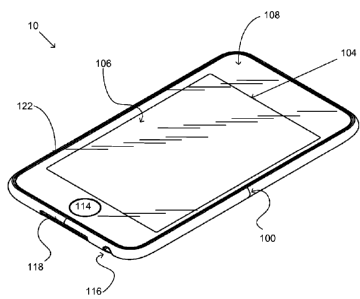
Unfortunately, increased weight may lead to user dissatisfaction, and bowing
may
damage the internal parts
[0004] Furthermore, in most portable electronic devices, the enclosures are
mechanical assemblies having multiple parts that are screwed, bolted, riveted,
or
otherwise fastened together at discrete points. For example, the enclosures
typically
have included an upper casing and a lower casing that are placed on top of one
another and fastened together using screws. These techniques typically
complicate
the housing design and create aesthetic difficulties because of undesirable
cracks,
seams, gaps or breaks at the mating surfaces and fasteners located along the
surfaces
of the housing. For example, a mating line surrounding the entire enclosure is
produced when using an upper and lower casing. Not only that, but assembly is
often
1
CA 02735999 2011-03-03
WO 2010/027565 PCT/US2009/050879
a time consuming and cumbersome process. For example, the assembler has to
spend
a certain amount of time positioning the two parts and attaching each of the
fasteners.
Furthermore, assembly often requires the assembler to have special tools and
some
general technical skill.
[0005] Another challenge is in techniques for mounting structures within
the
portable computing devices. Conventionally, the structures have been laid over
one
of the casings (upper or lower) and attached to one of the casings with
fasteners such
as screws, bolts, rivets, etc. That is, the structures are positioned in a
sandwich like
manner in layers over the casing and thereafter fastened to the casing. This
methodology suffers from the same drawbacks as mentioned above, i.e., assembly
is a
time consuming and cumbersome.
[0006] Therefore, it would be beneficial to provide a portable
electronic
device that is aesthetically pleasing and lightweight, yet durable. It would
also be
beneficial to provide methods for assembling the portable electronic device.
SUMMARY OF THE INVENTION
[0007] The invention relates, in one embodiment, to a handheld
electronic
device. The handheld electronic devices includes at least a single seamless
housing
having a front opening and a cover disposed within the front opening and
attached to
the seamless housing without a bezel.
[0008] The invention relates, in another embodiment, to seamless housing
formed of a single sheet of metal. The seamless housing includes a top
opening, an
integral bottom and side walls that cooperate to form a cavity in cooperation
with the
top opening, the bottom wall having a curved bottom surface, the side walls
being
rounded such that they form a curved side surface and an undercut within the
cavity,
an inside edge of the side walls surrounding and defining the top opening, and
an
outside edge, a mounting bracket attached to the bottom wall suitable for
securing an
electronic assembly to the bottom wall of the housing and an opening in at
least one
sidewall having a depth of trim at least greater than that provided by the
housing
alone.
[0009] The invention relates to in another embodiment to a small form
factor
electronic device that includes at least a seamless housing having an integral
bottom
and side walls that cooperate to form a cavity in cooperation with a front
opening
having a flat top surface, the bottom wall having a curved bottom surface, the
side
2
CA 02735999 2011-03-03
WO 2010/027565 PCT/US2009/050879
walls being rounded such that they form a curved side surface and an undercut
within
the cavity, an edge of the side walls surrounding and defining the front
opening and a
plurality of electronic assemblies inserted into the seamless housing through
the front
opening and secured to the bottom surface of the housing, wherein a Z height
tolerance of the plurality of electronic assemblies is minimized such that an
upper
surface of a topmost electronic assembly is substantially coplanar with the
flat top
surface of the housing.
[0010] A method of self centering a topmost glass unit in a small
form factor
electronic device is also disclosed. The small form factor electronic device
is formed
of a seamless housing having a front opening having a flat top surface and
side walls
where an edge of the side walls surrounds and defines the front opening and
wherein
the glass unit includes an environmental seal having a tapered portion,
wherein at
least some of the tapered portion of the environmental seal extends beyond an
inner
edge of the front opening. The method can be carried out by,
inserting the glass
unit into the front opening and self aligning the glass unit during the
insertion by,
interacting of the inner edge of the front opening that the portion of the
environmental
seal that extends beyond the inner edge of the opening, and concurrently with
the
interacting of the inner edge and the extended portion of the environmental
seal, glass
unit fasteners cooperating with a lead in device.
[0011] In another embodiment an integrated speaker assembly suitable for
use
in a small form factor portable hand held device is described. The integrated
speaker
assembly includes at least a piezoelectric speaker arranged to produce at
least audible
sounds, an acoustic seal having a plurality of acoustic seal gaps that work in
cooperation with the piezoelectric speaker to direct the sound produced by the
piezoelectric speaker to a desired location in the small form factor portable
hand held
device, and an acoustic barrier arranged to prevent audible sounds leaking to
undesired locations in the small form factor electronic device.
[0012] The invention relates to in another embodiment to a minimum Z
height
mounting bracket system to secure an operational component in a handheld
computing device having a seamless enclosure. The mounting bracket includes a
plurality of sacrificial z adjustment bumps having a sacrificial portion
arranged along
the length of the mounting bracket wherein after the mounting bracket is
attached to
the seamless enclosure, a top portion of the seamless enclosure and the
sacrificial
3
CA 02735999 2013-06-25
portion of the sacrificial z adjustment bumps are machined off concurrently
with
a drilling a plurality of xy alignment holes, wherein the machining and the
drilling are performed in a single machine set up thereby minimizing alignment
tolerance in xy and z directions.
[0013] The invention relates in another embodiment to a method of
centering a racetrack between a formed edge and an inside edge of a
seamless enclosure used for supporting a handheld computing device. The
method is carried out by optically determining a plurality of reference points
on
the formed edge of the seamless enclosure and cutting the inside edge using
the plurality of optical reference points.
[0014] The invention relates in another embodiment to a method of
centering a racetrack between a formed edge and an inside edge of a
seamless enclosure having a single open end, wherein the seamless enclosure
supports a handheld computing device having display portion located in the
single open end. The method is carried out by determining a center point of
the
display portion, determining an angle of tilt of the display portion, and
cutting
the inside edge based upon the center point and the angle of tilt.
[0014a] The invention relates to another embodiment to a handheld
electronic device, comprising: a single seamless metal housing having a front
opening, the single seamless housing having an integral bottom and side walls
that cooperate to form a cavity in cooperation with the front opening, the
side
walls being rounded such that they form a curved side surface and an undercut
within the cavity; and a cover glass disposed within the front opening and
attached to the seamless housing using the undercut; a display unit disposed
within the cavity of the metal housing; a display screen of the display unit
being
visible through the cover glass; and a substantially transparent touch sensing
layer disposed between the cover glass and the display screen of the display
unit.
[0014b] In another embodiment the invention relates to a handheld
electronic device, comprising: a single seamless housing having a front
opening and an integral bottom and side walls that cooperate to form a cavity
in
cooperation with the front opening, the bottom wall having a curved bottom
4
CA 02735999 2013-06-25
surface, the side walls being rounded such that they form a curved side
surface
and an undercut within the cavity, an inside edge of the side walls
surrounding
and defining the front opening; and a cover disposed within the front opening
and attached to the seamless housing without a bezel.
[0014c] In a still further embodiment the invention relates to a handheld
electronic device, comprising: a single seamless metal housing having a front
opening; and a cover glass disposed within the front opening and attached to
the seamless housing without a bezel; and a racetrack, the racetrack being a
region between a formed edge and an inside edge of the seamless housing
wherein the racetrack is centered with respect to the formed edge by
determining a center point of the display portion, determining an angle of
tilt of
the display portion, and cutting the inside edge based upon the center point
and the angle of tilt.
[0014d] In a further embodiment the invention relates to a small form
factor electronic device, comprising: a seamless housing having an integral
bottom and side walls that cooperate to form a cavity in cooperation with a
front
opening having a flat top surface, the bottom wall having a curved bottom
surface, the side walls being rounded such that they form a curved side
surface
and an undercut within the cavity, an edge of the side walls surrounding and
defining the front opening; and a plurality of electronic assemblies inserted
into
the seamless housing through the front opening and secured to the bottom
surface of the housing, wherein a Z height tolerance of the plurality of
electronic
assemblies is minimized such that an upper surface of a topmost electronic
assembly is substantially coplanar with the flat top surface of the housing
wherein the plurality of electronic assemblies includes a first electronic
assembly comprising: a first electronic sub assembly, a second electronic
subassembly, and a substantially planar flex circuit that operatively and
physically connects the first and second electronic subassemblies, the flex
circuit including cut outs which allow the flex circuit to twist so that the
flex
circuit can conform to a curved shape in multiple dimensions.
4a
CA 02735999 2015-02-11
[0014e] In a still further aspect, the present invention provides a
handheld
electronic device, comprising: a single piece housing component having a front
opening, the housing component having a bottom wall and side walls that
cooperate to
form a cavity in cooperation with the front opening; a cover glass disposed
within the
front opening, the cover glass comprising a first frame member attached to the
cover
glass; a display unit disposed within the cavity of the housing component so
that a
display screen of the display unit is visible through the cover glass; and a
second frame
member attached to an inside surface of the housing component, wherein the
first frame
member is retained by the second frame member such that the cover glass is
centered
and secured within the front opening of the housing component.
BRIEF DESCRIPTION OF THE DRAWINGS
[0015] The invention will be readily understood by the following
detailed
description in conjunction with the accompanying drawings, wherein like
reference
numerals designate like structural elements, and in which:
[0016] Figs. lA ¨ 1B are perspective diagrams of a handheld computing
device
in its assembled form.
[0017] Fig. 1C is a cross sectional view of the housing highlighting
the nature of
the undercut geometry.
[0018] Figs. 2A ¨ 2E are an exploded perspective diagrams of an electronic
device in its unassembled form.
[0019] Figs. 3A ¨ 3B are view diagrams of the housing showing the
racetrack.
[0020] Figs. 4A ¨ 4B graphically illustrate centering a racetrack in
accordance
with an embodiment of the invention.
[0021] Figs. 5A ¨ 5C show low Z height integrated speaker system suitable
for
use in a small form factor electronic device.
[0022] Figs. 6A ¨ 6B show audio jack opening in accordance with an
embodiment of the invention.
4b
CA 02735999 2013-06-25
WO 2010/027565 PCT/US2009/050879
[0023] Figs. 7A ¨ 7C show assembly of G unit in accordance with an
embodiment of the invention.
[0024] Figs. 8A ¨ 8B show gas relief structures in accordance with an
embodiment of the invention.
[0025] Fig. 9 shows a representative cross sectional view of the housing
where the dock opening formed by folding over a portion of the housing in
accordance with an embodiment of the invention.
[0026] Figs. l OA ¨ 10B shows a representative cross sectional view of
the
housing where the dock opening is to be created by way of a
punching/forming/machining process.
[0027] Figs. 11A ¨ 11C graphically illustrate the process for forming
a short
span opening in the housing.
[0028] Figs. 12A ¨ 12C graphically illustrate the process for forming
a long
span opening in the housing.
[0029] Fig. 13 shows a comer stiffener in accordance with an embodiment of
the invention
[0030] Fig. 14 shows representative sacrificial z alignment bumps pre
and
post machining.
[0031] Fig. 15 shows a flowchart detailing a process for installing
mounting
brackets into a housing in accordance with an embodiment of the invention.
[0032] Fig. 16 shows a flowchart detailing a process for assembling
the device
in accordance with an embodiment of the invention.
DETAILED DESCRIPTION OF THE EMBODIMENTS
[0033] Reference will now be made in detail to a preferred embodiment
of the
invention. An example of the preferred embodiment is illustrated in the
accompanying drawings. While the invention will be described in conjunction
with a
preferred embodiment, it will be understood that it is not intended to limit
the
invention to one preferred embodiment. To the contrary, it is intended to
cover
alternatives, modifications, and equivalents as may be included within the
scope of the invention as defined by the appended claims.
[0034] The described embodiments relate to an aesthetically pleasing
portable
electronic device. The portable electronic device is formed of a curved
seamless
housing and an aesthetically pleasing polished flat top glass layer. The
uniformity of
5
CA 02735999 2011-03-03
WO 2010/027565 PCT/US2009/050879
the appearance of the portable electronic device is enhanced since unlike
conventional
portable electronic devices, the polished top glass layer is mounted to the
seamless
housing without the use of a bezel. The seamless nature of the housing and the
lack
of a bezel provide several advantages besides the uniform and appealing
appearance.
Such advantages include the fact that fewer components are required for
assembly,
the portable electronic device is able to more readily withstand the impact of
drop
event, and better protection is provided to the polished glass top layer and
any
sensitive operational components therein.
[0035] The seamless housing is formed from a single sheet of metal
(such as
stainless steel). The housing has an undercut geometry in which the linear
dimensions
of an opening into which the operational components are inserted during
assembly are
smaller than the linear dimensions of the body of the housing itself.
Moreover, the
curvature of the housing is asymmetric in that an upper portion of the housing
is
formed to have a deep spline (i.e., higher curvature) whereas a lower portion
of the
housing is formed to have a more shallow spline. This asymmetry aids in a
user's
tactile sensation in part because it provides a better fit to the user's hand.
Moreover,
the metallic nature of the housing provides good electrical grounding for
built-in RF
antenna as well as to mitigate the effects of electromagnetic interference
(EMI) and
electrostatic discharge (ESD).
[0036] Unlike the assembly of conventional portable electronic devices
where
components are assembled in a top-down manner (i.e., the components are
inserted
into the housing before the bezel is snapped on), the undercut geometry of the
housing
requires that all components fit within the smaller dimensions of the window
opening
in the housing. Moreover, the assembly of the portable electronic device is
carried
out in a bottom-up manner using what is referred to as a blind assembly. In
order to
facilitate the bottom-up, blind assembly of the portable electronic device and
to
minimize any offsets between the polished top glass layer and an uppermost
portion
of the housing (referred to as the racetrack), various techniques, apparatus
and
systems are presented that minimize stack (i.e., z direction) tolerance. For
example,
portions of brackets used to mount subassemblies are welded to the housing and
are
subsequently machined at the same time and with the same set up as a topmost
portion of the housing. In this way accurate Z datums for mounting various
components are provided. It should be noted that machining is preferred since
6
CA 02735999 2011-03-03
WO 2010/027565 PCT/US2009/050879
machined tolerances on the order of 0.05 mm can be achieved whereas
conventional
weldment position tolerances are typically on the order of 0.2 mm.
[0037] Other aspects of the invention relate to specific approaches
to
minimizing the Z height of the assembled components. In other words, in
keeping
with both the aesthetic look and feel, the Z height of the portable electronic
device is
maintained to a value consistent with providing a favorable user experience.
This can
be accomplished in a number of ways in addition to those already discussed
with
regards to, for example, the mounting brackets. A minimum Z height speaker
assembly can be fabricated using a piezoelectric speaker in combination with a
horizontal acoustic barrier. Gaps in the horizontal acoustic barrier have the
effect of
directing the sound produced by the piezoelectric speaker to any desired
location in
the housing. For example, the sound can be directed to specific openings in
the
housing otherwise unrelated to the broadcasting of sound. Such openings can
include
for example a dock opening and/or an audio jack opening. Enhancing the
perceived
sound by providing a back volume (i.e., using the back surface of the housing
as a
resonator) can be achieved using existing components and an appropriately
placed
back volume acoustic seal. In order to assure that the back volume seal
integrity is
maintained in spite of the variance in Z tolerance between the shield and
housing
changes from device to device, adapters are placed in close proximity to the
back
volume acoustic seal.
[0038] Other aspects of the invention that preserve the available Z
height
relate to the organization of circuits associated with the battery and display
screen. In
particular, as described below battery and display screen circuitry co-exist
in the same
Y location thereby reducing the overall Y component of the circuits. In the
described
embodiments, the battery circuitry can include a battery safety circuit and
the display
circuitry can include a display controller (in the particular embodiments, the
display is
a liquid crystal display, LCD, and the controller is a LCD controller).
Conventional
designs dictate that the battery safety circuit be placed in a central portion
of the
battery and that the LCD controller not be aligned to a far edge of the
display (this
would likely increase line width and parasitic capacitance reducing the
available drive
of the LCD controller). Furthermore, in order to conform to the spline of the
housing
and to reduce the overall Z of the product, the CD controller flex is bent
around the
battery.
7
CA 02735999 2011-03-03
WO 2010/027565 PCT/US2009/050879
[0039] Furthermore, providing gas relief structures on a plastic
frame used to
mount the protective glass layer enhances the adhesion of glass layer to
plastic frame.
Such structures can be formed by, for example, removing predetermined sections
of
plastic frame in appropriate locations by punching holes of a predetermined
size and
location. In this way, any trapped gases, such as air, can escape providing a
more
uniform distribution of adhesive resulting in a stronger and more reliable
bond
between the glass layer and the plastic frame.
[0040] These and other embodiments of the invention are discussed
below
with reference to Figs. 1-16. However, those skilled in the art will readily
appreciate
that the detailed description given herein with respect to these figures is
for
explanatory purposes as the invention extends beyond these limited
embodiments.
[0041] Throughout the following discussion, the term "CNC" is used.
The
abbreviation CNC stands for computer numerical control and refers specifically
to a
computer controller that reads computer instructions and drives a machine tool
(a
powered mechanical device typically used to fabricate components by the
selective
removal of material). It should be noted however, that any appropriate
machining
operation can be used to implement the described embodiments and is not
strictly
limited to those practices associated with CNC.
[0042] Figs. 1A ¨ 1B are perspective diagrams showing various views
of fully
assembled portable electronic device 10 in accordance with an embodiment of
the
invention. The portable electronic device 10 may be sized for one-handed
operation
and placement into small areas such as a pocket, i.e., the portable electronic
device 10
can be a handheld pocket sized electronic device. By way of example, the
electronic
portable electronic device 10 may correspond to a computer, media device,
telecommunication device and/or the like. The portable electronic device 10 is
capable of processing data and more particularly media such as audio, video,
images,
etc. The portable electronic device 10 may generally correspond to a music
player,
game player, video player, personal digital assistant (PDA), and/or the like.
With
regards to being handheld, the portable electronic device 10 can be operated
solely by
the user's hand(s), i.e., no reference surface such as a desktop is needed. In
some
cases, the handheld device is sized for placement into a pocket of the user.
By being
pocket sized, the user does not have to directly carry the device and
therefore the
8
CA 02735999 2011-03-03
WO 2010/027565 PCT/US2009/050879
device can be taken almost anywhere the user travels (e.g., the user is not
limited by
carrying a large, bulky and heavy device).
[0043] The portable electronic device 10 may be widely varied. In
some
embodiments, portable electronic device 10 may perform a single function
(e.g., a
device dedicated to playing and storing media) and, in other cases, the
electronic
device may perform multiple functions (e.g., a device that plays/stores media,
receives/ transmits telephone calls/text messages/internet, and/or performs
web
browsing). In some embodiments, the portable electronic device 10 is capable
of
communicating wirelessly (with or without the aid of a wireless enabling
accessory
system) and/or via wired pathways (e.g., using traditional electrical wires).
In some
embodiments, the portable electronic device 10 may be extremely portable
(e.g., small
form factor, thin, low profile, lightweight). In some cases, the portable
electronic
device 10 may be sized for being handheld. The portable electronic device 10
may
even be sized for one-handed operation and placement into small areas such as
a
pocket, i.e., the portable electronic device 100 can be a handheld pocket
sized
electronic device.
[0044] By way of example, the portable electronic device 10 may
correspond
to consumer electronic products such as computers, media players, personal
digital
assistants (PDA), telecommunication devices (phone), personal e-mail or
messaging
devices and/or the like. In one example, the electronic device may correspond
to any
of those electronic devices an iPodTM, an iPod NanoTM, an iPod ShuffleTM, an
iPodTM
Touch or an iPhoneTM available by Apple Inc. of Cupertino, California.
[0045] The portable electronic device 10 includes a housing 100
configured to
at least partially enclose any suitable number of components associated with
the
electronic portable electronic device 10. For example, the housing may enclose
and
support internally various electrical components (including integrated circuit
chips
and other circuitry) to provide computing operations for the device. The
integrated
circuit chips and other circuitry may include a microprocessor, memory, a
battery, a
circuit board, I/0, various input/output (I/0) support circuitry and the like.
Although
not shown in this figure, the housing 100 may define a cavity within which the
components may be positioned and housing 100 also may physically support any
suitable number of mechanisms, within housing 100 or within openings through
the
surface of housing 100.
9
CA 02735999 2011-03-03
WO 2010/027565 PCT/US2009/050879
[0046] In addition to the above, the housing may also define at least
in part the
outward appearance of portable electronic device 10. That is, the shape and
form of
the housing 100 may help define the overall shape and form of the portable
electronic
device 10 or the contour of the housing 100 may embody the outward physical
appearance of the portable electronic device 10. Any suitable shape may be
used. In
some embodiments, the size and shape of the housing 100 may be dimensioned to
fit
comfortably within a user's hand. In some embodiments, the shape includes a
slightly
curved back surface and highly curved side surfaces. The shape will be
described in
greater detail below.
[0047] In one embodiment, the housing 100 is integrally formed in such as
way as to constitute is a single complete unit. By being integrally formed,
the
housing 100 has a seamless appearance unlike conventional housings that
include two
parts that are fastened together thereby forming a reveal, a seam there
between. That
is, unlike conventional housings, the housing 100 does not include any breaks
thereby
making it stronger and more aesthetically pleasing.
[0048] The housing 100 can be formed of any number of materials
including
for example plastics, metals, ceramics and the like. In one embodiment,
housing 100
can be formed of stainless steel in order to provide an aesthetic and
appealing look
and feel as well as provide structural integrity and support for all sub-
assemblies
installed therein. When metal, the housing 100 can be formed using
conventional
collapsible core metal forming techniques well known to those skilled in the
art.
[0049] The portable electronic device 10 also includes a cover 106
that
includes a planar outer surface. The outer surface may for example be flush
with an
edge of the housing wall that surrounds the edge of the cover. The cover 106
cooperates with the housing 100 to enclose the portable electronic device 10.
Although the cover can be situated in a variety of ways relative to the
housing, in the
illustrated embodiment, the cover 106 is disposed within and proximate the
mouth of
the cavity of the housing 100. That is, the cover 106 fits into an opening
108. In an
alternate embodiment, cover 106 may be opaque and may include touch sensing
mechanism that forms a touch pad. Racetrack 122 is defined as the uppermost
portion
of the housing 100 that surrounds the polished top glass layer 106. In order
to
maintain the desired aesthetic look and feel of the portable electronic device
10, it is
CA 02735999 2011-03-03
WO 2010/027565 PCT/US2009/050879
desirable that any offsets between the housing 100 and the polished top glass
layer
106 be minimized and the racetrack 122 be centered.
[0050] The cover 106 may be configured to define/carry the user
interface of
the electronic device 10. The cover 106 may for example provide a viewing
region
for a display screen 104 used to display a graphical user interface (GUI) as
well as
other information to the user (e.g., text, objects, graphics). The display
screen 104
may be part of a display unit (not shown) that is assembled and contained
within the
housing 100. The display unit may for example be attached internally to a
metal
frame (e.g., 302). The cover may also provide a user clickable input button
114 (home
button) that can be used to provide a user input event to the portable
electronic device
10. Such user input events can be used for any number of purposes, such as
resetting
the portable electronic device 10, selecting between display screens presented
on
display screen 104, and so on. In one embodiment, the cover 106 is a
protective top
layer of transparent or semitransparent material (clear) such that the display
screen
104 is visible therethrough. That is, the cover 106 serves as a window for the
display
screen 104 (i.e., the transparent cover overlays the display screen). In one
particular
embodiment, the cover is formed from glass (e.g., cover glass), and more
particularly
highly polished glass. It should be appreciated, however, that other
transparent
materials such as clear plastic may be used.
[0051] In one embodiment, the viewing region may be touch sensitive for
receiving one or more touch inputs that help control various aspects of what
is being
displayed on the display screen. In some cases, the one or more inputs can be
simultaneously received (e.g., multi-touch). In these embodiments, a touch
sensing
layer (not shown) can be located below the cover glass 106. The touch sensing
layer
may for example be disposed between the cover glass 106 and the display
screen104.
In some cases, the touch sensing layer is applied to the display screen 104
while in
other cases the touch sensing layer is applied to the cover glass 106. The
touch
sensing layer may for example be attached to the inner surface of the cover
glass 106
(printed, deposited, laminated or otherwise bonded thereto). The touch sensing
layer
generally includes a plurality of sensors that are configured to activate as
the finger
touches the upper surface of the cover glass 106. In the simplest case, an
electrical
signal is produced each time the finger passes a sensor. The number of signals
in a
given time frame may indicate location, direction, speed and acceleration of
the finger
11
CA 02735999 2011-03-03
WO 2010/027565 PCT/US2009/050879
on the touch sensitive portion, i.e., the more signals, the more the user
moved his or
her finger. In most cases, the signals are monitored by an electronic
interface that
converts the number, combination and frequency of the signals into location,
direction, speed and acceleration information. This information may then be
used by
the portable electronic device 10 to perform the desired control function
relative to the
display screen 104.
[0052] The portable electronic device 10 can also include one or more
switches including power switches, volume control switches, user input devices
and
the like. A power switch 110 can be configured to turn the portable electronic
device
10 on and off, whereas a volume switch 112 is configured to modify the volume
level
produced by the electronic portable electronic device 10. portable electronic
device
lOportable electronic device 10The portable electronic device 10 may also
include
one or more connectors for transferring data and/or power to and from the
portable
electronic device 10. The portable electronic device 10 may includes an audio
jack
116 and a data/power connector 118. The audio jack 116 allows audio
information to
be outputted from the portable electronic device 10 by way of a wired
connector. The
connector 118 allows data to be transmitted and received to and from a host
device
such as a general purpose computer (e.g., desktop computer, portable
computer). The
connector 118 may be used to upload or down load audio, video and other image
data
as well as operating systems, applications and the like to and from the
portable
electronic device 10. For example, the connector 118 may be used to download
songs
and play lists, audio books, photos, and the like into the storage mechanism
(memory)
of the portable electronic device 10. The connector 118 also allows power to
be
delivered to the portable electronic device 10.
[0053] The connector 118 can receive an external corresponding connector
(not shown) that is capable of plugging into a host device (and/or power
supply) in
order to allow communications (e.g., data/power transfer) between the portable
electronic device 10 and the host device. The connector may be widely varied.
In
one embodiment, the connector is a peripheral bus connector, such as a USB or
FIREWIRE connector. These type of connectors include both power and data
functionality, thereby allowing both power delivery and data communications to
occur between the portable electronic device 10 and the host device when the
portable
electronic device 10 is connected to the host device. In some cases, the host
device
12
CA 02735999 2011-03-03
WO 2010/027565 PCT/US2009/050879
can provide power to the media portable electronic device 10 that can be used
to
operate the portable electronic device 10 and/or charge a battery included
therein
concurrently with the operating. In one particular embodiment, the connector
is a 30
pin connector as used in many products manufactured by Apple Inc of Cupertino,
CA.
Audio jack 116 can receive an audio post (not shown) that can provide audio
signals
to external audio rendering devices, such as headphones, speakers, etc.
[0054] Although the device may connect through various wired
connections, it
should be appreciated that this is not a limitation. In one embodiment, the
electronic
portable electronic device 10 also includes a mechanism for wireless
communications.
For example, as shown, the portable electronic device 10 may include an
antenna (i.e.,
antenna 222). The antenna may be disposed internal to the housing 100. The
wireless communications can be based on many different wireless protocols
including
for example Bluetooth, RF, 802.11, and the like. In order to minimize any
adverse
impact on wireless communications in embodiments where the housing is metallic
and therefore conductive, portable electronic device 10, a portion of the
housing 100
may replaced with a radio transparent cap 120 formed of a non-conductive
material,
such as plastic.
[0055] Fig. 1C shows a cross sectional view of the housing 100
highlighting
the nature of the undercut geometry. Although in general the inner cross
sectional
shape of the housing 100 may be the same or different from the external cross
sectional shape of the housing 100, the interior shape of housing 100
substantially
conforms to the outer shape of housing 100. The housing 100 can be formed
having
an undercut geometry with curvature that more easily receives the hand of a
user (e.g.,
form fits). In particular, an interior wall of housing 100 substantially
conforms to the
shape of an exterior wall of housing 100. More specifically, side wall 121
(both
interior and exterior) is rounded and curved inwardly to form a concave
undercut
region 123 formed at an upper portion of the side wall 121 in proximity to cut
edge
128. By undercut it is meant that the side wall 121 curves back inwardly
towards the
interior of the housing 100. In this way, the window opening 108 has at least
smaller
X dimension and Y dimension than does the body of the housing 100. In one
example, the housing 100 can have dimensions of approximately (x,y)housing =
(61.8
mm, 111 mm) whereas the opening 108 can have dimensions of approximately
(X,Y)opening = (58.3 mm, 107.5 mm).
13
CA 02735999 2011-03-03
WO 2010/027565 PCT/US2009/050879
[0056] Figs. 2A ¨ 2E show various exploded perspective diagrams of
the
electronic portable electronic device 10 in its unassembled form. The portable
electronic device 10 includes housing 100 shown in Fig. 2A into which are
attached a
number of operational and/or structural components. Housing 100 can take the
form
of a seamless enclosure. The seamless nature of the housing 100 provides an
aesthetic look and feel to the portable electronic device 10 as well as
provides added
resistance to deformation and possible damage to internal components caused by
the
impact of a drop event. In the embodiments described herein, housing 100 is
formed
of stainless steel and having thickness of approximately 0.5 mm. It should be
noted,
however, that this configuration is representative in nature only and does not
provide
limitations constraining the ultimate scope of the invention.
[0057] The housing 100 extends along a vertical (Y) axis and a
horizontal (X)
axis having a height Z. The housing 100 can be of various sizes. For example,
the
housing 100 can have a height (Z) of approximately 8.5 mm, an X dimension of
approximately 61.8 mm and a Y dimension of approximately 111 mm. The housing
100 includes a cavity 124 which is sized and dimensioned for the receipt of
the
internal components of the portable electronic device 10. The internal
components
are assembled through window opening 108. The undercut geometry of the housing
100 provides that the linear dimensions of the window opening 108 into which
the
operational components are inserted during assembly are smaller than the
linear
dimensions of the body of the housing 100. For example, the window opening 108
can have an X dimension of approximately 58.3 mm and a Y dimension of
approximately 107.5 mm.
[0058] One aspect of the desired look and feel is the symmetry in
design and
conformal appearance of portable electronic device 10. One aspect of the
symmetry
of the portable electronic device 10 concerns the racetrack 122. The racetrack
122 is
the strip of metal around the cover 106 on the front face of the device. The
width of
the racetrack 122 is defined by an outer racetrack profile and inner racetrack
profile.
Since the housing 100 is made from a sheet metal material, the outer racetrack
profile
is achieved by sheet metal forming while the inner racetrack profile is
achieved by
machining where the forming tolerance is much greater than machining
tolerance. In
the described embodiment, the outer racetrack profile is consistent with a
formed edge
126 whereas the inner racetrack profile is consistent with and cut edge 128 of
housing
14
CA 02735999 2011-03-03
WO 2010/027565 PCT/US2009/050879
100 as illustrated in Fig. 3 showing a representative cross section and top
view of
portable electronic device 10 highlighting the relationship of racetrack 122
and both
the formed edge 126 and the cut edge 128.
[0059] In order to maintain the desired appearance of portable
electronic
device 10 it may be desirable to properly center racetrack 122. This centering
can
however be accomplished in a number of ways depending upon what is considered
to
be an important factor in the overall aesthetics of the design of portable
electronic
device 10. In any case, a series of optical measurements are made using for
example
a CCD camera to measure the outside racetrack profile after a rough cut of
same.
Once the CCD measurements have been taken, any of a number of approaches can
be
used to center the racetrack 122. However, depending upon which approach is
taken
can result in somewhat different results. For example, as shown in Fig. 4A,
centering
the racetrack 122 using the outside racetrack profile (i.e., formed edge 126)
will
produce a consistent racetrack width, however, the gap 130 from the housing to
glass
will be less consistent. On the other hand, the racetrack 122 can also be
centered by
forming the inner racetrack profile shape by cutting the cut edge 128 per the
3D CAD,
but use the CCD measurements to find the center (xo, yo) and any rotation
angle cp for
cutting the inner profile as shown in Fig. 4B. This particular centering
approach will
give a less consistent racetrack width but a more consistent gap 130 from the
housing
to glass.
[0060] Figs. 2B ¨ 2E illustrate the operational components of the
portable
electronic device 10. In the described embodiment, the components of the
portable
electronic device 10 are organized in layers. The relationship and
organization of the
components within each layer and relationship between layers can be used to
facilitate
both the assembly and optimization of Z height tolerances of the portable
electronic
device 10. By minimizing Z height tolerances, the electronic portable
electronic
device 10 is manufactured to be extremely compact, sturdy, aesthetically
pleasing and
ergonomic at relatively low cost. For example, the fact that the electronic
portable
electronic device 10 is assembled without the need of a bezel reduces
manufacturing
and assembly costs. The layers can include a first (main electronic) layer
200, a
second (metal frame or M-frame) layer 300 and a third (glass or G unit) layer
400
each of which is described in more detail below.
CA 02735999 2011-03-03
WO 2010/027565 PCT/US2009/050879
[0061] Fig. 2B shows a detailed view of the first layer 200 (referred
to
hereinafter as PCB layer 200) in accordance with an embodiment of the
invention.
[0062] The PCB layer 200 includes a first assembly 204 and a second
assembly 206, which are physically and operatively connected via a flex
circuit 202.
The first assembly 204 includes a printed circuit board (PCB) 205 onto which
the flex
circuit 202 is attached. The printed circuit board 205 is configured to carry
multiple
components including for example processor, memory and the like. The printed
circuit board 205 is also configured to carry an RF shield 207 that is
disposed over the
various components. RF shield 207 is formed from metal and configured to cover
and
surround the components. The first assembly also includes a speaker system 209
that
is not a separate discrete system but rather a system that integrates with
other
components in order to properly output sound. At its core, the speaker system
includes a piezo speaker 210, acoustic seal 212 and acoustic barrier. The
piezo
speaker 210 is attached to the RF shield 207, the acoustic seal 212 closes off
gaps in
order to form an acoustic volume between RF shield and housing. This
embodiment
will be described greater detail in Figs. 5A-5C. The printed circuit board 205
is also
configured to carry the connector 118 and the audio jack assembly 116. In the
described embodiment, the audio jack 116 fits into audio jack opening 117 and
acts as
an interface to an external circuit (such as head or earphones) by way of a
wire or
other type connector. For proper fit of the audio jack 116 into the audio jack
opening
117, the audio jack opening 117 must have a shape that conforms to both the
spline of
the housing 100 as well as the shape of the audio jack 116 described in more
detail in
Figs. 6A ¨ 6B.
[0063] The PCB layer 200 can be fitted into cavity 124 of housing 100
and
secured to an interior wall of the housing 100 using fasteners such as screws
208a and
208b that connect directly to housing 100 (it should be noted that screw 208b
also
facilitates RF antenna grounding discussed in more detail below). It should be
noted
that prior to assembly, the power button 110 is attached to the housing using
a power
button plate 228 and the volume button 112 is attached to the housing 110
using a
volume button plate 230 each of which are electrically connected to each other
by
way of flex 232.
[0064] One of the problems with having an active RF antenna assembly
in a
close proximity to a number of active circuits is the generation of
electromagnetic
16
CA 02735999 2011-03-03
WO 2010/027565 PCT/US2009/050879
interference (EMI) that can detune or otherwise adversely affect the
performance of
the RF antenna 222. For example, the relatively long conductors present in the
flex
202 can act as a source of EMI that can detrimentally affect the performance
of RF
antenna 222. In order to substantially reduce or even eliminate this source of
EMI it
would be desirable to RF ground the PCB 200. Therefore, in order to provide a
good
RF ground, portions 226 of the insulating layer of flex 202 facing the inside
surface of
housing 100 are removed in order to expose the conductive layer therein. The
portions 226 of the flex 202 that are removed typically are those regions that
are
relatively large and contiguous thereby having the greatest potential to
provide good
RF grounding when placed in contact with the metal of housing 100. In the
described
embodiment, after the portions 226 of the flex 202 have been removed, the
exposed
conductive material is pressed down onto the housing 100. The presence of
pressure
sensitive conductive adhesive (PSCA) placed between flex 202 and housing 100
provides the requisite mechanical and electrically conductive bond. In
addition to
providing good RF grounding, the conformance of the flex 202 to the inside
surface
of housing 100 reduces the overall Z profile of the PCB 200.
[0065] Figs. 2C and 2D show a un-assembled top view and an assembled
bottom view of third layer 300 referred to hereinafter as metal (M) frame
assembly
300, respectively, in accordance with an embodiment of the invention. Turning
first
to Fig. 2C, M-frame assembly 300 can include M-frame 302, battery 304 attached
to
the M-frame 302 by way of pressure sensitive adhesive (PSA) and display
circuit 306
that includes display 104. In the described embodiment, Z height requirements
for the
M-frame 300 can be reduced by using what is referred to as half shears 310.
Half
shears 310 can be formed by removing portions of the M-frame 302 in those
locations
around screw holes in M-frame 300 used to accommodate screws 312a and 312b
that
attach M-frame 302 to housing 100. In the described embodiment, a sufficient
amount of material is removed from M-frame 302 such that a top portion of each
of
the screws 312a and 312b are essentially flush with a top surface 314 of the M-
frame
302. As described in more detail below, each half shear 310 is aligned with a
Z
height datum bump described in more detail below thereby further minimizing Z
height requirements for portable electronic device 10. Moreover, display unit
alignment holes 316 are provided to accept alignment pins (not shown) on
display
17
CA 02735999 2011-03-03
WO 2010/027565 PCT/US2009/050879
unit 306 that provide x,y alignment to the housing 100 by way of alignment
holes 140
in mounting brackets 136a and 136b.
[0066] In addition to minimizing Z height requirements, the overall Y
component of battery circuits and display circuits can be reduced as shown in
Fig. 2D
that graphically illustrates the organization of circuits associated with the
battery 304
and display circuit 306. In particular, battery circuitry 318 and display
circuitry 320
co-exist in the same Y location thereby reducing the overall Y component of
the
circuits. In the described embodiments, the battery circuitry 318 can take the
form of
a battery safety circuit 318 and the display circuitry can include a LCD
controller 320.
Conventional designs dictate that the battery safety circuit 318 be placed in
a central
portion of the battery 304 and that the LCD controller 320 should not be
aligned to a
far edge of the display circuit 306 (as this would likely increase line width
and
parasitic capacitance reducing the available drive of the LCD controller).
However,
by modifying the design of both battery safety circuit 318 and LCD controller
320,
the two circuits can be placed at the same Y location. In this way, the
overall Y
component of the two circuits taken together can be reduced. Furthermore, in
order to
conform to the spline of the housing 100 and to reduce the overall Z of the
portable
electronic device 10, the LCD controller flex 322 is wrapped around and placed
under
the battery 304 in order for display connector 324 and battery connector 326
to mate
as shown in Fig. 2D.
[0067] Portable electronic device 10 includes glass, or G, unit 400
shown in
Fig. 2E. G unit 400 includes cover glass 106. G unit 400 also includes cover
glass
PSA 404 used to adhere cover glass 106 plastic frame 406. Environmental seal
408
can be used to prevent dust or other unwanted environmental contaminants from
entering the portable electronic device 10 after assembly. During assembly, G
unit
400 can be placed within window 108 of housing 100 on top of the M-frame
assembly
300 as shown in Figs. 8A ¨ 8C. The G unit 400 self aligns during the insertion
process and secured to M frame 302 using M-frame lead in 324. G unit 400
includes
a double shot arrangement formed of plastic frame 406 and an environmental, or
cosmetic, seal 408 made of, for example, thermoplastic urethane (TPU), rubber,
and
the like that can act to protect portable electronic device 10 from dust and
or moisture.
As described below, the shape of environmental seal 408 in relation to housing
100
aids in self aligning G unit 400 to window 108 opening during assembly. During
the
18
CA 02735999 2011-03-03
WO 2010/027565 PCT/US2009/050879
assembly process as shown in Fig. 8A, the G unit 400 is inserted into window
opening
108 by bringing plastic frame 406 into contact with M-frame lead in 324. In
the
described embodiment, both the environmental seal 408 and the M-frame lead in
324
have corresponding tapered shapes that provide for the G unit 400 to self
align. For
example, in Fig 8B, as the G unit 400 is being inserted into the window
opening 108,
the plastic frame 406 encounters the tapered shape of the M-frame lead in 324.
The
M-frame lead in 324 has the effect of both aligning and securing the G unit
400 until
such time as shown in Fig. 8C that the tapered edge of the environment seal
408
encounters the inside, or cut edge, 128 of the housing 100. A portion 410 of
the
environmental seal 408 extends beyond the cut edge 128. In the described
embodiment, the portion 410 has a tapered edge that causes the G unit 400 to
self
center to the window opening 108 as shown in Fig. 8C until the G unit 400 is
captured
by M-frame lead in 324.
[0068] During assembly, when pressure is applied to G unit 400,
trapped
gases coalesce into gas bubbles having the result of minimizing the bond area
between the pressure sensitive adhesive (PSA) and the glass 106. The gas
become
trapped due in part to the fact that due to assembly tolerances, the PSA would
touch
the seal 402 closing off a gas escape route(see Fig. 9A). Therefore, it would
be
advantageous to provide gas relief structures or assembly techniques on
plastic frame
406 thereby enhancing the adhesion of glass layer 106 to plastic frame 406.
Gas relief
techniques can include removing predetermined sections of plastic frame 404 in
appropriate locations by for example punching holes of a predetermined size
and
location or by removing small amounts of PSA from corners of the portable
electronic
device 10 allows trapped gas to escape more easily as shown in Fig. 9B. In
this way,
a more uniform distribution of adhesive resulting in a stronger and more
reliable bond
between glass layer 106 and plastic frame 404 can be achieved.
[0069] Fig 5A shows an integrated, or minimum Z height speaker
assembly
500 which is a particular embodiment of the integrated speaker assembly shown
in
Fig. 2B. The minimum Z height speaker assembly 500 includes at least a
piezoelectric speaker 210 in combination with acoustic seal 212 and a
horizontal (Y)
acoustic barrier 502. Gaps 504 in the acoustic seal have the effect of
directing the
sound produced by the piezoelectric speaker 210 to any desired location in the
housing 100. For example, the sound can be directed to specific openings in
the
19
CA 02735999 2011-03-03
WO 2010/027565 PCT/US2009/050879
housing 100 otherwise unrelated to the broadcasting of sound. Such openings
can
include for example dock opening 119 and/or an audio jack opening 117. The
horizontal acoustic barrier 502 ensures that substantially no sound leaks to
undesired
portions of the housing 100 such as gaps associated with the volume button
112,
power button 110, or the antenna cap 120. Furthermore, as shown in Fig. 5B, a
back
volume seal 506 can form an acoustic cavity 508, also referred to as a back
volume, in
cooperation with the housing 100. In this way, by using existing components, Z
height requirements for creating the back volume 508 are reduced and a
backside
portion of the housing 100 can act as a resonator arranged to enhance the
audio
experience of a user. Since the back volume 508 is created using existing
components
(i.e., housing 100 and acoustic barrier 502), there is no adverse impact on
the overall
Z height of the portable electronic device 10.
[0070] Fig. 5C shows selected crush zones 510 that are provide for
adjustments for variations in Z tolerances and assure the integrity of the
back volume
508. During assembly of portable electronic device 10, pressure can be exerted
onto
PCB 200 that has the effect of compressing, or crushing, crush zones 510. In
this
way, any variations in Z height of the various components of PCB 200 can be
accommodated without comprising the integrity of the back volume 508. It
should be
noted that crush zones 510 can take on any of a number of shapes and sizes and
be
formed of any resilient material able to form a seal between the housing 100
and the
back volume seal 506.
[0071] As shown in Fig. 6A, one of the problems with the asymmetric
geometry of the housing 100 is that as the bottom cut surface (point "A") of
audio
jack opening 117 moves up in the positive Z direction, the edge of the cut
moves in a
negative Y direction due to the high curvature of the housing 100. In other
words, a
small change in the positive Z direction results in a large change in the
negative Y
direction. Since the audio jack 116 is fixed in the Z direction, the size of
the audio
jack opening 117 must not come so close to the upper portion of the housing
100 so as
to present a risk to the cover glass 106 as would be the case if the audio
jack opening
117 were formed too far into the shallower portion of the housing 100. In any
case,
having a fully circular portion in the shallower geometry of the housing 100
can result
in very sharp edges (as shown in Fig. 6A) that must be machined down.
Conventional
machining processes, however, would cause the housing 100 in that region to
become
CA 02735999 2011-03-03
WO 2010/027565 PCT/US2009/050879
unacceptably thin presenting a risk of damage in an impact event. Therefore,
in order
to accommodate the circular shape of audio jack 116, the spline of housing
100, as
well as to decrease the audio jack trim (the material around the audio jock
structure
itself) as little as possible, an non-symmetric audio jack opening 117 is
formed as
shown in Fig. 6B having circular portion 602 and a non circular portion 604
providing
the non-symmetric shape for audio jack opening 117. In this way, the audio
jack
opening 117 provides that the audio jack 116 and the audio jack opening
maintains a
centered and circular appearance especially when viewed from above. It should
be
noted that it has been discovered that subsequent to the forming of the audio
jack
opening 117 in this manner, a deburring process for touch up can be performed
using
materials considered unconventional in the art of deburring. Such materials
can
include, for example, a bamboo wooden stick, wooden chopsticks, and the like.
[0072] In order to accommodate various interfaces (dock, audio jack,
volume,
power, for example), openings of various sizes must be created in the housing
100.
There are a number of approaches that can be used to create these openings and
make
the opening trim appear to be thicker than the thickness (0.5 mm) of the sheet
metal
used to create the housing 100. One approach relies upon drawing or folding
the
sheet metal that forms the housing 100 as shown in Fig. 9. In any case,
creating these
openings in the housing 100 can result in long and thin webs of metal that can
deform
from the impact of a drop event, for example. In order to reinforce these
areas, any of
a number of different techniques can be used to add an additional layer of
material
(referred to as child material) to the parent material, which in this case is
stainless
steel having an approximate thickness of 0.5 mm. In some embodiments, the
child
material can be bonded to the parent material by welding, soldering, brazing
or
gluing. Once the child material is bonded to the parent material, a one stage
cut is
performed (machine or laser cut or punch, for example) in order to create the
actual
hole geometry.
[0073] Figs. 10A ¨ 10B shows a representative cross sectional view of
the
housing 100 in the area of the dock opening 119. However, due to the thickness
(approximately 0.5 mm), the material (stainless steel) from which the
described
housing is formed, and the geometry (i.e., deep spline) of the housing 100
obtaining
the desired deep cut is difficult to achieve in a large scale manufacturing
environment.
In particular, looking at Fig. 10A, due to the geometry of the housing 100
using a
21
CA 02735999 2011-03-03
WO 2010/027565 PCT/US2009/050879
conventional punching operation to create the dock opening 119 would result in
unacceptable asymmetric cut between the steep spline of the top portion and
shallower spline of the lower portion of housing 100. Therefore as illustrated
in Fig.
10A, a metal support bracket 1002 having a thickness approximately that of the
housing 100 (which in this embodiment is approximately .5 mm) can be attached
to
the inside wall of housing 100 using solder or braze material or glued. By
using
solder or braze material or glue, the support bracket 1002 can be securely
attached to
the housing 100 as well as provides a good cosmetic result since the solder or
braze
material obscures the gap between the housing 100 and support bracket 1002.
Fig.
10B shows a result of the punching operation to form the dock opening 119. By
using
the support bracket 1002, a double wall is formed in the area of the housing
100 in
which the dock opening 119 (or any opening in housing 100 for that matter). In
the
described embodiment, since any gaps between support bracket 1002 and housing
100
are filled with solder or braze, both the desired cosmetic appearance and the
desired
structural integrity and strength can be maintained. It should be noted that
in order to
provide optimal strength for holes having large spans (volume button opening),
the
respective support brackets are positioned such that the presumptive hole is
positioned
approximately midway of the support bracket.
[0074] Figs. 11A ¨ 11C graphically illustrate the process for forming
the dock
opening. Fig. 11A illustrates the placement of support bracket 1002 on housing
100
in relation to proposed dock opening 117. The support bracket 1002 can be
welded to
housing 100. Fig. 11B shows in profile view juxtaposition of support bracket
1002
and proposed dock opening. In this case, the support bracket 1002 covers the
entire
area of the proposed dock opening in order to provide maximum support post
CNC.
Accordingly, Fig. 11C shows in profile the post punching operation and CNC of
dock
opening 119, the support bracket 1002 having an upper portion 1102 and a lower
portion 1104. It should be noted that in order to cosmetically hide the gap
between
the support bracket and housing 100, solder or braze material can be used to
fill any
gaps post CNC.
[0075] In the case of openings having long spans, such as the volume
control
button, Figs. 12A ¨ 12C graphically illustrate the process for forming a long
span
opening such as the volume button opening. Fig. 12A illustrates the placement
of
support bracket 1202 on housing 100 in relation to proposed volume button
opening.
22
CA 02735999 2011-03-03
WO 2010/027565 PCT/US2009/050879
It should be noted that in this case, the support bracket 1202 only extends
approximately midway in the y direction since the primary area requiring
support is
that thin strip 1204 above the proposed volume control button. The thin strip
1204 is
susceptible to deformation during an impact event. Fig. 12B shows a profile
view of
the juxtaposition of the support bracket 1202, the housing 100, and the
proposed
location of the volume control button. Fig. 12C shows the post laser cut of
the
volume control button illustrating the upper support bracket providing the
requisite
support for any long span openings in housing 100 such as volume button.
[0076] It should be noted, however, that the above procedures are
predicated
on materials, such as stainless steel, and geometries (i.e., those have steep
splines) that
are not conducive to providing symmetric cuts or the proper depth of cut in a
punching type operation. However, it is contemplated that using material other
than
stainless steel, such as aluminum, can provide the requisite symmetry. In
these cases,
a one piece punch and CNC can be used. It should further be noted that the
thickness
of the support brackets can be varied but it is found that having a thickness
approximate to that of the housing 100 works well.
[0077] In order to prevent interference with RF antenna 222, housing
material
is removed from housing 100 to form antenna hole 126. The antenna hole 126 by
removing conductive housing material using a laser and replaced with non-
conducting
material such as plastic to form antenna cap 120. In this way, the
interference caused
by the presence of a conducting material such as metal in the immediate
vicinity of
RF antenna 222 is eliminated. However this cutting away may cause the corner
portion 128 of the housing 100 to become weakened to the point where it
becomes
susceptible to deformation or damage due to an impact event. Therefore, a
corner
stiffener 130 can be used to provide structural support for the corner portion
128 of
the housing 100 by reinforcing the sidewall of housing 100 of the corner
portion 128
as shown in Fig. 13. Corner stiffener 130 is welded to or otherwise attached
to
housing 100. However, in contrast to other support brackets such as those for
volume
button and dock, the corner stiffener 130 serves two purposes, one to provide
additional structural integrity to the corner 128 of housing 100 where
material is to be
removed and another as a ground for RF antenna 222. In the described
embodiment,
antenna ground 132 is connected to RF antenna 222 by way of antenna screw
208b. In
order to provide good electrical connection between RF antenna 222 and corner
23
CA 02735999 2011-03-03
WO 2010/027565 PCT/US2009/050879
stiffener 130, antenna ground 132 must remain substantially intact both in
order to
mechanically receive antenna screw 208b and provide good electrical contact to
corner stiffener 130 (and housing 100).
[0078] Due to the size and location of antenna hole 126, a laser is
used to
remove the necessary amount of material from the housing 100 to form the
antenna
hole 126. However, the antenna ground 132 extends into the region in close
proximity to the material to be lasered off. Since antenna ground 132 must
remain
relatively intact, antenna ground 132 is protected against any dross generated
by the
laser removing material to form the antenna hole 126 by a shield formed of for
example, foam, or any other protective material that can be easily removed
subsequent to the forming of antenna hole 126.
[0079] Returning to Fig. 2A showing a detailed view of housing 100.
As
shown, the housing 100 includes a number of attachment fixtures used for
attaching
subassemblies to housing 100. Such attachment features can include, for
example,
PCB subassembly securing fixtures 134a and 134b, and 134c that can be used to
attach PCB assembly 200 to housing 100 using fasteners such as screws 310b and
screw 208a, respectively. It should be noted that screws 310b attach M-frame
assembly 300 and PCB 200 to housing 100 using fixtures 134a and 134b unlike
screws 310a that attach M-frame assembly 300 directly to mounting brackets
136a
and 136b. As discussed above, RF ground 132 is used to both secure PCB 200 to
housing 100 as well as provide a ground plane for RF antenna 222.
[0080] Mounting brackets 136a and 136b are used to secure M-frame
subassembly 300 to housing 100. However, conventional approaches to attaching
mounting brackets to housing 100 utilize high temperature attaching processes,
such
as laser welding, that can and usually do result in cosmetic damage to the
exterior
surface of the housing 100. This cosmetic damage can require expensive and
time
consuming remediation, such as polishing, that can increase the cost of and
time
required to assembly the portable electronic device 10. Therefore, in order to
avoid
the creation of the cosmetic damage, only low temperature attachment processes
are
used to attach mounting brackets 136a and 136b to housing 100. In order to
eliminate
cosmetic damage caused by high temperature attachment processes (such as laser
welding), mounting brackets 136a and 136b are placed in appropriate locations
on
inside surface of housing 100 using a low temperature weld process. Once
24
CA 02735999 2011-03-03
WO 2010/027565 PCT/US2009/050879
positioned, mounting brackets 136a and 136b are securely attached to inside
surface
of housing 100 using a low temperature solder process. By using low
temperature
weld and solder processes, any damage, cosmetic or otherwise, to external
surface of
housing 100 that would have been caused by the attachment of mounting brackets
136a and 136b to housing 100 using conventional methods such as high
temperature
processes is eliminated. Therefore, in contrast to the conventional approach
of using
high temperature attachment processes, using low temperature attachment
processes
eliminates the necessity to perform a post attach polishing or other
remediation on the
exterior surface of the housing 100. In this way, the aesthetic look and feel
of
portable electronic device 10 is preserved. In this way, the mounting brackets
136a
and 136b provide reference surfaces for receiving and supporting some portion
of the
internal components. Furthermore, the mounting brackets 136a and 136b provide
Z
datum bumps 138 that minimize Z height, or stack, tolerance of the assembled
internal components discussed in more detail below.
[0081] During the assembly of portable electronic device 10, the PCB 200, M-
frame assembly 300 and G unit 400 are placed one atop the other during what is
referred to as a blind assembly operation in which each layer must align with
each
every other layer with minimum Z height tolerance. As well known in the art,
whenever a manufacturing operation requires a number of different setups, each
separate setup has an associated tolerance each of which is added to all the
other
tolerances. By minimizing the number of setups in a manufacturing operation,
the
total Z height tolerance for the operation can be kept to a minimum.
Therefore, in
order to minimize Z height tolerances in the assembly of portable electronic
device
10, a number of novel approaches have been devised. For example, in order to
minimize the Z height tolerance in attaching the M-frame assembly 300 to the
housing 100, the mounting brackets 136a and 136b include the aforementioned Z
datum bumps 138 (where two Z datum bumps are located on either side of M-frame
screw hole 146). It should be noted that the Z datum bumps 138, the machined
top
surface 140 of the housing 100, and display unit alignment holes 142 are
machined at
the same time using a single set up (as illustrated in Fig. 14). In this way,
a Z height
tolerance in relation to the top surface 140 of the housing 100 of
approximately .05
mm can be achieved (compared to a Z height tolerance of approximately .2 mm
using
a standard soldering approach with multiple set ups).
CA 02735999 2011-03-03
WO 2010/027565 PCT/US2009/050879
[0082] Fig. 15 shows a flowchart detailing a process 1500 for
installing
mounting brackets into a housing in accordance with an embodiment of the
invention.
The process 1500 begins at 1502 by providing mounting brackets having
sacrificial z
adjustment bumps located thereon. In the described embodiment, the z
adjustment
bumps are arranged to have a portion of which can be machined away during a
subsequent machining process during which a top portion of the housing is also
machined off. At 1504, the mounting brackets are positioned within the housing
using a low energy attachment process such as a low energy weld. Next at 1506,
the
positioned brackets are soldered in place. The following operations are
performed
during a single set up, where at 1508 the top portion of the housing is
machined off,
the sacrificial portion of the z adjustment bumps is removed at 1510, and
display unit
x,y alignment holes are drilled in the bracket at 1512.
[0083] Fig. 16 shows a flowchart detailing a process 1600 for
assembling the
portable electronic device 10 in accordance with an embodiment of the
invention.
Firstly, at 1602, a pre-assembled housing is received. In the described
embodiment,
the housing has had all appropriate openings formed, support brackets and
attachment
fixtures affixed thereto. At 1604, the PCB assembly is placed within the
housing
cavity. Since the window opening is smaller than the housing body, the
insertion of
the PCB assembly is done by inserting either the first or the second portion
first
followed by the remaining portion. For example, when inserting the PCB
assembly, if
the first portion of the PCB assembly is inserted first, then the dock and the
audio jack
are inserted into their appropriate openings in the housing. Once the dock and
the
audio jack are properly seated, then the second portion of the PCB assembly is
inserted, which in this case includes the RF antenna assembly. Once the PCB
assembly is in place, then a portion of the conductive layer of the flex
portion of the
PCB assembly is exposed at 1606. It should be noted that this step can be
performed
anytime prior to the insertion of the PCB into the housing. By exposing a
portion of
the conductive layer of the flex portion, an RF ground plane can be
established by the
housing. Once the conductive layer of the flex portion has been exposed, the
PCB
assembly is secured to the housing at 1608. In the described embodiment, the
PCB
assembly can be secured using screws to attach the first portion of the PCB
assembly
including the dock and the audio jack to the housing directly using PCB
attachment
fixtures. Once the PCB has been secured to the housing, the exposed conductive
layer
26
CA 02735999 2011-03-03
WO 2010/027565
PCT/US2009/050879
of the flex is conformally pressed to the inside surface of the housing at
1610. In the
described embodiment, pressure sensitive conductive adhesive can be used to
adhere
the exposed portions to the housing. In addition to providing a good
electrical contact
thereby providing a good RF ground, by pressing the flex onto the inside
surface of
the housing, the flex is mechanically secured to the housing and also the
amount of
space taken up by the flex is concomitantly reduced.
[0084] Once
the PCB is in place and secured, a pre-assembled M-frame and
battery are received at 1612. By pre-assembled it is meant that the battery
has already
been attached to the M-frame by way of the pressure sensitive adhesive (PSA).
At
1614, the display unit is placed upon the side of the M-frame opposite to that
of the
battery. It should be noted that the display unit is not attached to the M-
frame at this
point since the display unit must be tilted up in order to gain access to the
display flex.
The display flex is then placed under the battery and electrically connected
to the
battery electrical connector at 1616. Once the battery and the display unit
have been
electrically connected to each other, the M-frame assembly, including the
battery and
the display unit are secured to the housing using a number of available screws
at
1618. Again since the display unit is not attached directly to the M-frame,
the display
unit is lifted in order to gain access to the screw holes in the M-frame.
[0085] It
should be noted that in the described embodiment, a number of the
available screws used to attach the M-frame assembly to the housing utilize
mounting
brackets attached directly to the housing. These mounting brackets include a
number
of Z height datum bumps that provide a Z reference for M-frame assembly. In
addition, some of the remaining available screws are used to attach the M-
frame
assembly as well as the PCB to the housing. Once the M-frame has been secured
to
the housing, the display unit is aligned using a number of alignment pins
placed
diagonally from each other on either side of the display unit at 1620. The
alignment
pins can be used to mate with alignment holes in the mounting brackets. At
1622, the
touch panel is electrically connected to the battery and at 1624, the glass
unit is
inserted into the window opening and secured to the M-frame at 1626.
[0086] While this invention has been described in terms of several
preferred
embodiments, there are alterations, permutations, and equivalents, which fall
within
the scope of this invention. It should also be noted that there are many
alternative
ways of implementing the methods and apparatuses of the present invention. For
27
CA 02735999 2011-06-10
example, although a die cast process is preferred method of manufacturing the
seamless
enclosure, it should be noted that this is not a limitation and that other
manufacturing
methods may be used. It is therefore intended that the following appended
claims be
interpreted as including all such alterations, permutations, and equivalents
as fall within
the scope of the present invention.
[0087] The electronic device also includes a plurality of electronic
assemblies
inserted into the seamless housing through the front opening and secured to
the bottom
surface of the housing, wherein a Z height tolerance of the plurality of
electronic
assemblies is minimized such that an upper surface of a topmost electronic
assembly is
substantially coplanar with a top surface of the housing wherein the plurality
of
electronic assemblies. The first subassembly includes a first electronic sub
assembly, a
second electronic subassembly, and a substantially planar flex circuit that
operatively
and physically connects the first and second electronic subassemblies, the
flex circuit
including cut outs which allow the flex circuit to twist so that the flex
circuit can
conform to a curved shape in multiple dimensions. The second electronic
subassembly
includes an RF antenna, wherein a corner portion of the housing in close
proximity to
the RF antenna is removed in order to substantially eliminate EMI caused by
the
housing and replaced with an antenna cap formed of a non-RF interfering
material. The
antenna cap includes a corner portion stiffener arranged to reinforce the
corner portion
of the housing having the antenna cap, wherein the stiffener acts as a ground
plane for
the RF antenna wherein the stiffener includes a contact arranged to
electrically connect
the RF antenna with the ground plane formed by the stiffener.
[0088] A method can be performed by providing a single seamless
housing, the
single seamless housing having a front opening, an integral bottom and side
walls,
wherein the integral bottom and side walls cooperate to form a cavity in
cooperation
with the front opening, placing a cover unit within the front opening, the
cover unit
having a flat top surface and substantially filling the front opening, and
attaching the
cover unit to the seamless housing without a bezel. The integral bottom wall
has a
curved bottom surface, the side walls being rounded such that they form a
curved side
surface and an undercut within the cavity, an inside edge of the side walls
surrounding
and defining the front opening and the flat top surface is substantially flush
with an
upper surface of the inside edge of the side wall and wherein the cover unit
is attached
28
CA 02735999 2011-06-10
to a frame. Attaching the cover unit to the seamless housing without a bezel
can be
carried out by attaching the frame to the housing within the cavity. In the
described
embodiment, the cover unit includes a display unit having at least a display
screen, a
cover glass through which the display screen is visible, and a substantially
transparent
touch sensing layer disposed between the cover glass and the display screen
and the
housing is formed of polished stainless steel and the cover unit includes an
opening
suitable for receiving an input mechanism.
28a