Note: Descriptions are shown in the official language in which they were submitted.
CA 02736272 2011-03-04
WO 2010/039458 PCT/US2009/057458
1
LOW POWER ELECTRONIC SYSTEM USING NON-VOLATILE
MAGNETIC MEMORY
TECHNICAL FIELD
[0001] The present disclosure is related, in general, to
electronic circuit
architecture and, more particularly to a low power system architecture using
non-
volatile magnetic memory.
BACKGROUND
[0002] In today's electronics-driven world, power is the key to
keeping
society in motion. However, with the increasing costs of power and, in
handheld
devices, the demand for increased battery life, the issue of power consumption
in
electronic devices has become of paramount importance. When computers lay idle
for a
period of time, many enter a power-collapsed state or standby state, in which
power
consumption is dramatically reduced. Handheld devices, such as mobile phones,
when
not in use, typically also enter a power-collapsed state, in which the power
or battery is
disconnected from many parts of the operating circuitry. Electronic components
themselves have also been developed with lower power requirements. Taken as a
whole, a considerable amount of technology has been developed for conserving
power.
While power consumption has been considerably reduced using these
technologies,
electronics designers are still generally limited by the power requirements of
memory,
and, in particular, the power requirements of memory to save state.
[0003] Modern electronics are typically designed to "wake up,"
i.e.,
reestablish power when exiting from a standby state, without having lost any
of the
operational information in memory when the electronic device collapsed into
the
standby state. For example, a user who answers the phone in the middle of
writing a
letter in a word processor might leave the computer long enough for the
computer to
enter the standby mode. When the user comes back, he or she may wake the
computer
up and immediately continue writing the letter from the point at which he/she
left off
Similarly, when a user reaches for his or her phone to make a call, the phone
typically
wakes up from its standby state (if the user was not currently using the
phone), ready to
receive dialing and make the call. Also, if a user is playing video using a
digital signal
processor (DSP) of a mobile device and a call arrives, causing the DSP to
power
collapse, the user should be able to return to the same video playback state
after the call
CA 02736272 2011-03-04
WO 2010/039458 PCT/US2009/057458
2
is completed or ignored. The user is not required to cold start the devices
and reload
the information from a disk drive or other external non-volatile memory
storage in
either of these examples. In order to accomplish this instant-on
functionality, the
information or application state is generally preserved even though the
electronics have
had power substantially reduced. The power is only moderately reduced because
power
is generally needed to preserve the information in the memory. While other
components may be completely shut down or removed from the power supply, there
is a
certain amount of power that is usually always-on in order to keep the memory
blocks
from losing the information that is held.
[0004] Many electronic systems utilize static random access memory
(SRAM) and dynamic random access memory (DRAM) because of their speed and
density. However, SRAM and DRAM are both volatile memories, meaning they lose
their information when power is removed. Thus, in order to maintain the state
of
SRAM and DRAM memories, power is maintained. One method for overcoming this
always-on power state has been to incorporate flash memory into the electronic
system.
Flash memory is a non-volatile memory technology that will maintain its
information
when the power is removed. However, flash memory is generally too slow to
replace
SRAM and DRAM memories, so it is often used as an external storage point to
store
state information.
[0005] FIGURE 1 is a block diagram illustrating an electronic
system 10
featuring a typical memory configuration using a flash non-volatile memory
106. The
system 10 is illustrated with an internal section 100 and an external section
101. The
external section 101 is generally connected to the internal section 100 within
the device.
The illustrated components of the system 10 are connected via a bus 102. The
SRAM
memory block 103 provides local memory for the logic block 104 which includes
various combinational logic components and latches using a system clock. A
DRAM
memory block 105 is provided in the external section 101 for local, yet
external to the
processing core of internal section 100, higher-volume random access storage
for the
system 10. The system 10 also includes a flash non-volatile memory (NVM) 106.
[0006] For purposes of the example illustrated in FIGURE 1, the
system
will be described as a system for use in a mobile phone. When the mobile phone
of
system 10 enters into the standby mode, all of the state information currently
stored in
the SRAM 103 and/or logic 104 is moved to the DRAM 105 on the same package. In
CA 02736272 2011-03-04
WO 2010/039458 PCT/US2009/057458
3
one embodiment, the state information could be stored off chip into the flash
NVM 106
from the DRAM 105. In this case the state information is encrypted incurring
additional time and energy.
[0007] Thus, power from the battery of the mobile phone is used to
scan
the SRAM 103 and logic 104 for state information, and move that state
information into
the DRAM 105 over the bus 102. Additional power is used to then move the state
information from the DRAM 105 over the bus 102 into the flash NVM 106.
Conventionally, the amount of power consumed by transmission of data over a
bus is a
function of the length of the bus. Thus, a considerable amount of power is
being
drained from the battery to move all of the state information. Moreover,
because flash
memory is much slower to write than SRAM and DRAM memories, this process takes
a
considerable amount of time, relative to mobile phone functionality. This is
not the
only power and time usage during standby processing. When the mobile phone of
the
system 10 powers back up, power is drained from the battery again to re-
install the state
information back from the flash NVM 106 to the DRAM 105 (if the NVM 106 is
actually used), and to the SRAM 103 and logic 104 from the DRAM 105. Thus,
while
the standby mode of the system 10 may consume less power because power is no
longer
used to maintain state in either the SRAM 103 or logic 104, a considerable
amount of
power is used transferring the state information to and from the DRAM 105 and
possibly the flash NVM 106, in addition to the considerable time used in
transferring
that information back and forth.
SUMMARY
[0008] Representative embodiments of the present disclosure relate
to
computing systems including at least one functional unit and a
magnetoresistive random
access memory (MRAM) block coupled to the at least one functional unit. The
MRAM
block is configured to store a functional state of the functional unit during
a power
down state of the functional unit.
[0009] Additional representative embodiments of the present
disclosure
relate to methods including receiving a standby signal requesting one or more
functional
units of a computing system to enter a standby state, storing, responsive to
receiving the
standby signal, at least a portion of a current operational state of the
functional units in a
magnetic random access memory (MRAM) coupled to the functional units, and
CA 02736272 2014-01-17
74769-3360
4
removing power from a power supply to the functional units after the current
operational state
is stored.
[00101 Further representative embodiments of the present disclosure
relate to systems
that include means for receiving a standby signal requesting one or more
functional units of a
computing system to enter a standby state, means, responsive to the standby
signal, for storing
at least a portion of a current operational state of the functional units in a
magnetic random
access memory (MRAM) coupled thereto, and means for removing power from the
functional
units after the current operational state is stored. The systems further
include means for
receiving a wake-up signal requesting the one or more functional units in the
standby mode to
enter an operating mode, means, responsive to the wake-up signal, for
restoring the power to
the functional units in the standby mode, and means for reinstating the
current operational
state to the functional units.
[0010a] According to an aspect of the invention, there is provided a
computing system
comprising: an internal section; an external section coupled to the internal
section; at least one
functional unit within the internal section; a magnetoresistive random access
memory
(MRAM) block within the internal section and embedded in a substrate of the at
least one
functional unit, the MRAM block configured to store a functional state of the
at least one
functional unit during a standby state of the internal section; and a volatile
memory within the
external section.
[0010b] According to another aspect of the invention, there is provided a
method
comprising: receiving a standby signal within a computing system including an
internal
section, and an external section coupled to the internal section, the standby
signal requesting
the internal section, including one or more functional units, to enter a
standby state during
operation of the external section; responsive to receiving the standby signal,
storing a first
portion of a current operational state from the one or more functional units
in a magnetic
random access memory (MRAM) embedded in a substrate of the one or more
functional units,
and storing, in the MRAM, a second portion of the current operational state
from the internal
CA 02736272 2014-09-22
74769-3360
4a
section; and removing power from the internal section including the one or
more functional
units after the current operational state is stored.
[0010c] According to still another aspect of the invention, there is
provided a system
comprising: means for receiving a standby signal within a computing system
including an
internal section and an external section coupled to the internal section, the
standby signal
requesting the internal section, including one or more functional units, to
enter a standby state
during operation of the external section; responsive to the standby signal,
means for storing a
first portion of a current operational state of the one or more functional
units in a magnetic
random access memory (MRAM) embedded in a substrate of the one or more
functional units,
and means for storing, in the MRAM, a second portion of the current
operational state from
the internal section; means for removing power from the internal section,
including the one or
more functional units after the current operational state is stored; means for
receiving a wake-
up signal requesting the one or more functional units in the standby mode to
enter an
operating mode; responsive to the wake-up signal, means for restoring the
power to the one or
more functional units in the standby mode; and means for reinstating the
current operational
state to the one or more functional units.
[0010d] According to yet another aspect of the invention, there is
provided a computing
system comprising: an internal section; an external section coupled to the
internal section; at
least one functional unit within the internal section; means for placing the
internal section into
a standby state during operation of the external section; and means for
storing a functional
state of the at least one functional unit, prior to placing the internal
section into the standby
state, during operation of the external section, the storing means within the
internal section
and embedded in a substrate of the at least one functional unit, wherein the
means for storing
the functional state of the at least one functional unit is configured to
store the functional state
of the at least one functional unit as a resistance value.
[0010e] According to a further aspect of the invention, there is
provided a computing
system comprising: an internal section; an external section coupled to the
internal section; at
least one functional unit within the internal section; a magnetoresistive
random access
memory (MRAM) block stacked on the internal section and coupled to the at
least one
CA 02736272 2014-09-22
74769-3360
4b
functional unit with a plurality of through substrate vias (TSVs), the MRAM
block configured
to store a functional state of the at least one functional unit during a
standby state of the
internal section; and a volatile memory within the external section.
[0010f] According to still a further aspect of the invention, there is
provided a method
comprising: receiving a standby signal within a computing system including an
internal
section, and an external section coupled to the internal section, the standby
signal requesting
the internal section, including one or more functional units, to enter a
standby state during
operation of the external section; responsive to receiving the standby signal,
storing a first
portion of a current operational state from the one or more functional units
in a magnetic
random access memory (MRAM) coupled to the one or more functional units, and
storing, in
the MRAM, a second portion of the current operational state from the internal
section; and
removing power from the internal section including the one or more functional
units after the
current operational state is stored.
[0010g] According to yet a further aspect of the invention, there is
provided a system
comprising: means for receiving a standby signal within a computing system
including an
internal section and an external section coupled to the internal section, the
standby signal
requesting the internal section, including one or more functional units, to
enter a standby state
during operation of the external section; responsive to the standby signal,
means for storing a
first portion of a current operational state of the one or more functional
units in a magnetic
random access memory (MRAM) coupled to the one or more functional units, and
means for
storing, in the MRAM, a second portion of the current operational state from
the internal
section; means for removing power from the internal section, including the one
or more
functional units after the current operational state is stored; means for
receiving a wake-up
signal requesting the one or more functional units in the standby mode to
enter an operating
mode; responsive to the wake-up signal, means for restoring the power to the
one or more
functional units in the standby mode; and means for reinstating the current
operational state to
the one or more functional units.
[0010111 According to another aspect of the invention, there is
provided a computing
system comprising: an internal section; an external section coupled to the
internal section;
CA 02736272 2014-09-22
= 74769-3360
4c
means for placing the internal section into a standby state during operation
of the external
section; and means for storing a functional state of the internal section,
prior to placing the
internal section into the standby state, during operation of the external
section, the storing
means being stacked on the internal section and coupled to the internal
section with a plurality
of through substrate vias, wherein the means for storing the functional state
of the internal
section is configured to store the functional state of the internal section as
a resistance value.
[0010i] According to still another aspect of the invention, there is
provided a
computing system comprising: a plurality of functional blocks, each functional
block
including a functional unit, and a magnetoresistive random access memory
(MRAM) block
coupled to the functional unit, the MRAM block configured to store an
operational state of the
functional unit during a standby state of the functional block including the
functional unit;
wherein the computer system is adapted to place one of the functional blocks
in a standby
state when another of the functional blocks is in a power on state.
[0010j] According to yet another aspect of the invention, there is
provided a method of
operating a computing system, including a plurality of functional blocks,
comprising:
receiving a standby signal requesting one functional block including one
functional unit, of a
computing system to enter a standby state; responsive to receiving the standby
signal, storing
a portion of a current operational state of the functional unit in a magnetic
random access
memory (MRAM) within the one functional block, the MRAM being coupled to the
functional unit; and removing power from the one functional block including
the functional
unit after the current operational state is stored when another functional
block is placed in a
power on state.
[0011] The foregoing has outlined rather broadly the features and
technical advantages
of the present invention in order that the detailed description of the
invention that follows may
be better understood. Additional features and advantages of the invention will
be described
hereinafter which form the subject of the claims of the invention. It should
be appreciated by
those skilled in the art that the conception and specific embodiments
disclosed may be readily
utilized as a basis for modifying or designing other structures for carrying
out the same
purposes of the present invention. It should also be realized by those skilled
in the art that
CA 02736272 2014-09-22
74769-3360
4d
such equivalent constructions do not depart from the scope of the invention as
set forth in the
appended claims. The novel features which are believed to be characteristic of
the invention,
both as to its organization and method of operation, together with further
objects and
advantages will be better understood from the following description when
considered in
connection with the accompanying figures. It is to be expressly understood,
however, that
each of the figures is provided for the purpose of illustration and
description only and is not
intended as a definition of the limits of the present invention.
BRIEF DESCRIPTION OF THE DRAWINGS
[0012] For a more complete understanding of the present disclosure,
reference is now
made to the following descriptions taken in conjunction with the accompanying
drawings, in
which:
CA 02736272 2011-03-04
WO 2010/039458 PCT/US2009/057458
[0013] FIGURE 1 is a block diagram illustrating an electronic
system
featuring a conventional memory configuration using a flash non-volatile
memory;
[0014] FIGURE 2, a block diagram illustrating of an electronic
system
configured in accordance with the teachings of the present disclosure;
[0015] FIGURE 3 is a block diagram illustrating another electronic
system configured in accordance with the teachings of the present disclosure;
[0016] FIGURE 4 is a block diagram illustrating a further
electronic
system configured in accordance with the teachings of the present disclosure;
[0017] FIGURE 5 is a block diagram illustrating a still further
electronic
system configured in accordance with the teachings of the present disclosure;
[0018] FIGURE 6 is a schematic diagram illustrating a side view of
an
electronic system configured in accordance with the teachings of the present
disclosure;
[0019] FIGURE 7 is a block diagram illustrating an electronic
system
configured in accordance with the teachings of the present disclosure; and
[0020] FIGURE 8 is a flow chart illustrating example blocks
executed to
implement various embodiments in accordance with the teachings of this
disclosure.
DETAILED DESCRIPTION
[0021] Turning now to FIGURE 2, a block diagram is illustrated of
an
electronic system 20 configured according to one embodiment of the present
disclosure.
The electronic system 20 has an internal section 200, in which processing
operations
internal to the functionality of the electronic system 20 or a particular
feature are
performed, and an external section 201, which is connected to the internal
section 200
and provides various functionalities, such as input/output (I/0), longer term
random
access storage, such as the DRAM block 205, and the like, which are performed
or
intended to be performed external to the internal section 200. The electronic
system 20
may have several internal sections or functional blocks, such as the internal
section 200,
providing various features and functionalities.
[0022] The electronic system 20 also provides for a spin torque
transfer
(STT) magnetic random access memory (MRAM) block 206 which provides an
internal
non-volatile memory. The STT MRAM block 206 uses magnetic polarity and not
charge storage to maintain its memory. Therefore, when the power supply 208 is
disconnected from the STT MRAM block 206, the memory state is retained because
the
CA 02736272 2011-03-04
WO 2010/039458 PCT/US2009/057458
6
magnetic polarity is maintained without reliance on power or electrical charge
or current
from power supply 208. Thus, when the internal section 200 enters into the
standby
state, the state information from the SRAM 203 and logic 204 is stored in the
STT
MRAM block 206. Moreover, because the STT MRAM block 206 is within the
internal
section 200, the amount of power consumed in transferring the data over the
bus 202 is
less than that consumed with regard to the electronic system 10 (FIGURE 1).
The STT
MRAM block 206 also reads and writes much faster than external non-volatile
memory,
such as a hard drive or flash memory, e.g., the flash NVM 106 of the
electronic system
(FIGURE 1). Therefore, still more power is saved because the amount of time it
takes to write the information to the STT MRAM block 206 is much less.
[0023] Once the state information has been transferred into the
STT
MRAM block 206, all or substantially all of the power from the power supply
208 can
be removed from the internal section 200, because the STT MRAM block 206 does
not
need power in order to maintain its data. When the internal section 200 powers
back up,
the power supply 208 is restored and the state information is re-loaded from
the STT
MRAM block 206 back into the SRAM 203 and logic 204. Again, because of the
shorter distance to travel on the bus 202 and the greater speed with which the
STT
MRAM block 206 reads and writes data, the state information is quickly loaded
back
into the SRAM 203 and logic 204 such that processing of the application can
continue
in what appears to the user to be a much more instantaneous manner and having
conserved a considerable amount of power during the standby state.
[0024] In operation, the electronic system 20 is a mobile phone.
The
internal section 200 is the multimedia section of the mobile phone. When a
call comes
into the mobile phone while the user is working in the multimedia section,
that section
is power-collapsed by turning the power supply 208 off to the internal section
200 and
is placed into a standby mode while the user answers the call. The telephony
functionality facilitating the user's phone call would then be implemented by
another
internal section (not shown) of the electronic system 20. When the call is
completed
and the user wants to return to his or her work in the multimedia section, the
internal
section 200 is powered up by restoring the power supply 208, as noted above.
During
its standby period, however, virtually no power leakage or consumption occurs
within
the internal section 200 because power is not required during the standby
state for the
CA 02736272 2011-03-04
WO 2010/039458
PCT/US2009/057458
7
STT MRAM block 206 to maintain the state information with regard to the
multimedia
processing.
[0025] In an additional and/or alternative embodiment of the
present
disclosure, a data mover block 207 is added to the internal section 200. The
data mover
block 207 is specifically tasked with moving the data from the SRAM 203 into
the STT
MRAM 206. The data mover block 207 includes a list of addresses which are
sequenced through when moving the data from the SRAM 203 to the STT MRAM 206
and back again. Inclusion of the data mover block 207 allows the transfer of
the data to
occur more rapidly.
[0026] FIGURE 3 is a block diagram illustrating an electronic
system 30
configured according to one embodiment of the present disclosure. In the
illustrated
embodiment, the electronic system 30 comprises a digital media player. The
electronic
system 30 is similar to the electronic system 20 (FIGURE 2), including an
internal
section 300, an external section 301, and a bus 302 coupling each of the
system
components. The internal section 300 includes an SRAM block 303 and an MRAM
block 306. The external section 301 includes a DRAM block 305. The electronic
system 30 also includes a multi-core logic 304. The multi-core logic 304
includes
multiple logic cores, 304-1 to 304-N that handle parallel or cooperative
processing of
data for the electronic system 30. The internal section 300 is powered by a
power
supply 307 which is coupled to the internal section 300 through a switch 308.
[0027] As the internal section 300 is powered down into a standby
state
the state information residing within the SRAM 303 and multi-core logic 304 is
quickly
stored within the MRAM block 306. In operation, any particular blocks with
MRAM
block 306 may be associated with a particular one of logic cores 304-1 to 304-
N.
Again, because of the speed with which the MRAM elements of the MRAM block 306
read and write data, and the shorter bus length of the bus 302 that the state
information
travels between the SRAM 303/multi-core logic 304 and MRAM block 306, a lesser
amount of power is consumed in storing the state of the internal section 300
than in the
electronic system 10 (FIGURE 1). Once the state is stored, the power supply
307 can
then be removed from the internal section 300 by opening the switch 308 during
the
standby state. Thus, virtually no power leakage or consumption occurs during
standby.
When the internal section 300 wakes up from standby, the switch 308 is again
closed,
restoring the power from the power supply 307. The reverse process restores
the state
CA 02736272 2011-03-04
WO 2010/039458 PCT/US2009/057458
8
information to the SRAM 303 and the multi-core logic 304 and the internal
section 300
continues processing at the same point as when it entered standby.
[0028] The embodiments illustrated in FIGURES 2 and 3 have shown
use of nonvolatile magnetic memory in separate components coupled together in
the
same internal section. However, additional and/or alternative embodiments of
the
present disclosure provide that the nonvolatile magnetic memories can be
integrated into
the same silicon substrate as the logic cores.
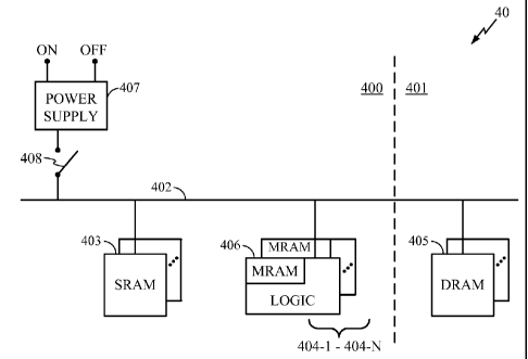
[0029] FIGURE 4 is a block diagram illustrating an electronic
system 40
configured according to one embodiment of the present disclosure. In the
illustrated
embodiment, the electronic system 40 is a desktop computer. The electronic
system 40
includes an internal section 400 and an external section 401. The external
section 401
includes a DRAM block 405. The internal section 400 includes an SRAM block 403
and a multi-core logic 404 and is powered by a power supply 407 coupled to the
internal
section 400 via a switch 408. The multi-core logic 404 includes an embedded
MRAM
406 in each of the logic cores 404-1 to 404-N. Because of the desirable
scalability and
compatibility with existing chip technology, the MRAM 406 can be embedded
directly
into the silicon substrate of the multi-core logic 404 with the addition of as
little as two
masks. In contrast, embedding flash memory into a logic core silicon substrate
generally uses as many as ten or more additional masks than the number of
masks
conventionally used to manufacture the other logic. In one embodiment, the
embedded
MRAM 406 is shared among some of the logical cores 404-1 to 404-N, and only
actually embedded in some of those logical cores 404-1 to 404-N.
[0030] With the embedded MRAM 406, the power consumed in
transferring the state information is much less than having to transfer it all
over the bus
402. Moreover, because the embedded MRAM 406 is on-chip, the number of I/0
paths
are not limited as when moving between components off-chip. Thus, the delay in
transferring the data is reduced because the bandwidth of the on-chip bus is
much higher
than bus 402. When the internal section 400 enters a standby state, the data
making up
the current operational state is saved onto the embedded MRAM 406 and the
power
supply 407 is shut off and isolated from internal section 400 by opening the
switch 408.
As the internal section 400 wakes up, the switch 408 is closed and the power
supply 407
is turned on, powering up the components of the internal section 400. The data
for the
current operational state is then reinstituted to the SRAM 403 block and the
multi-core
CA 02736272 2011-03-04
WO 2010/039458 PCT/US2009/057458
9
logic 404. Power consumption and time for the reading and writing processes
are,
therefore, greatly reduced.
[0031] FIGURE 5 is a block diagram illustrating an electronic
system 50
configured according to one embodiment of the present disclosure. The
electronic
system 50 is configured having a single-core logic 501 coupled with a SRAM
block 500
over a bus 502. Similar to the multi-core logic 404 (FIGURE 4), an MRAM block
503
is embedded directly into the silicon substrate of the single-core logic 501.
The
embedding of the MRAM 503 within the single-core logic 501 provides a
beneficial
relationship, as described with respect to the multi-core logic 404 (FIGURE
4).
Processing time and power are conserved because of the increased I/0 bandwidth
and
the resulting increased efficiency in on-chip data transmission. When the
electronic
system 50 enters the standby state, the power may be completely removed from
the
electronic system 50 and the state will still be retained in the MRAM 503.
[0032] When the MRAM components are embedded into a substrate of
the underlying logic circuitry, the MRAM configuration is designed with
respect to the
underlying logic configuration in order to facilitate the embedding. MRAM
blocks that
are fabricated within their own chips can be designed specifically to optimize
the
operation of the MRAM components. Thus, while directly embedding MRAM into the
silicon substrate of logic components will increase the speed and efficiency
of any data
transfer, an MRAM-only chip may be designed that reads and writes much faster
and
more efficiently than the embedded MRAM. Each such embodiment will have its
own
benefits depending on the desired operation of the system designer. In one
embodiment, both embedded MRAM and stand alone MRAM blocks (such as FIGURE
3) attached via bus are provided to achieve the benefits of both
configurations.
[0033] FIGURE 6 is a schematic diagram illustrating a side view of
an
electronic system 60 configured according to one embodiment of the present
disclosure.
The electronic component 60 is an integrated circuit including an MRAM chip
601
stacked on top of a logic chip 600. The MRAM chip 601 is connected to the
logic chip
600 through a series of interchip connectors 602, which comprise through
silicon vias
(TSVs) 603 and connector pads 604 in the depicted embodiment. The TSVs 603
allow
signals to be transmitted directly from the logic chip 600 to the MRAM chip
601. In
another embodiment (not shown) the MRAM and logic chips stacked within a
package
are interconnected using wire bonds, instead of TSVs. In both embodiments, the
power
CA 02736272 2014-01-17
74769-3360
savings is greatly increased over the transmission power consumption exhibited
in the
electronic system 10 of FIGURE 1 transmitting data over the bus 102. As
described
with respect to FIGURES 2-5, the MRAM chip 601 is able to save its information
and
maintain that information even when power is removed. Thus, the operation of
the
electronic system 60 provides for stable non-volatile storage of information
from the
logic chip 600.
[0034] The stacked-chip configuration of the electronic component 60
provides operation similar to the combined operation of MRAM and logic cores
described in FIGURES 2-5. In fact, in order to create additional and/or
alternative
embodiments, the electronic component 60 may be substituted for other MRAM-
logic
configurations. For example, the electronic component 60 may be substituted
for the
logic 204 and STT MRAM 206 of FIGURE 2; it may be substituted for each of the
MRAM blocks 306 and each of the logic cores 304-1 to 304-N of FIGURE 3; it may
be
substituted for each of the logic cores 404-1 to 404-N and the embedded MRAM
blocks
406 of FIGURE 4; and it may be substituted for the logic 501 and the embedded
MRAM 503 of FIGURE 5. The various embodiments of the present disclosure are,
thus, not limited to any particular configuration of MRAM blocks with regard
to the
particular electronic systems.
[0035] Turning now to FIGURE 7, FIGURE 7 is a block diagram
illustrating an electronic system 70 configured according to one embodiment of
the
present disclosure. The electronic system 70 is a multi-core logic block 700,
a RAM
block 701, and an STT MRAM block 702. In the embodiment of the electronic
system
70 depicted in FIGURE 7, the STT MRAM block 702 is used only to store state
information for the RAM block 701. The state information in the multi-core
logic block
700 is stored within non-volatile memory within each of latches 703 and 706.
The
technology underlying this non-volatile memory latch storage is described in
greater
detail in commonly-assigned, co-pending. U.S patent application serial number
12/328,042 entitled "NON-VOLATILE STATE RETENTION LATCH",
which has issued as U.S Patent No. 7,961,502.
[0036] , The multi-core logic block 700 includes latches 703 and 706
coupled with combinational logic blocks 704 and 705. By using the nonvolatile
magnetic memory configurations described in the incorporated patent
application, for
CA 02736272 2011-03-04
WO 2010/039458
PCT/US2009/057458
11
the nonvolatile memories 707 and 708, both the state information contained
within the
RAM block 701 and the state information contained within the multi-core logic
block
700 can be stored and maintained while power is removed from the electronic
system
70. Thus, the electronic system 70 may enter into a power-saving standby state
while
still maintaining the state information for an instant-on when the user
decides to wake
up the system. Therefore, little to no power is consumed or leaked while
electronic
system 70 is in standby mode because no power is required by the STT MRAM
block
702 or the nonvolatile memories 707 and 708 within multi-core logic blocks
700.
[0037] FIGURE 8 is a flowchart illustrating example blocks
executed to
implement one embodiment of the present disclosure. In block 800, a standby
signal is
received requesting one or more functional units of a computing system to
enter a
standby state. A functional unit is a set of registers and combinational logic
that
performs a basic function. For example, functional units include integer
units,
multimedia units (e.g., a video audio CODEC), etc. Responsive to receiving the
standby signal, at least a portion of a current operational state of the
functional units is
stored, in block 801, in a magnetic random access memory (MRAM) coupled to the
functional units. Power is removed, in block 802, from the one or more
functional units
after the current operational state is stored. A wake-up signal is received,
in block 803,
requesting the functional units in the standby mode to enter an operating
mode.
Responsive to receiving the wake-up signal, power is restored, in block 804,
from the
power supply to the functional units in the standby mode. The current
operational state
is reinstated in block 805 to the functional units.
[0038] It should be noted that while the illustrated embodiments
of the
present disclosure have been identified as a mobile phone, digital media
player, and
desktop computer, the various embodiments are not limited to these
implementations.
The present disclosure may take the form or any number of electronic systems
that
process something and has a processing state that may be maintained.
[0039] For purposes of this disclosure an MRAM block is considered
a
storage element in which data is not stored as electric charge or current
flows, but by
magnetic storage elements. The magnetic elements are generally formed from two
ferromagnetic plates, each of which can hold a magnetic field, separated by a
thin
insulating layer. In one embodiment, one of the two plates is a permanent
magnet set to
CA 02736272 2014-01-17
74769-3360
12
a particular polarity. The magnetic field of the other plate can be configured
to change
to match that of an external field. An MRAM block is built from a grid of such
"cells".
[0040] Whereas some embodiments presented herein are described with
respect to magnetic random access memory, and more particularly spin torque
transfer
(STT) magnetic random access memory, the features described can be
contemplated as
being applied as well to such devices including phase-change random access
memory
(PCRAM), resistance-based random access memory (R-RAM), or any device that can
store a resistance-based electrically programmable memory state in a non-
volatile
manner, i.e., in the absence of sustaining power, which is reprogrammable to a
plurality
of states, whether by electrical, magnetic, electromagnetic (e.g., optical),
or a
combination of such physical effects.
[0041] Although the present invention and its advantages have been
described in detail, it should be understood that various changes,
substitutions and
alterations can be made herein without departing from the scope of the
invention as defined by the appended claims. For example, although the
preceding
description has discussed replacing certain types of memory, such as the DRAM
or non-
volatile RAM, the disclosure is not limited to such embodiments. Rather,
portions of
each type of memory can remain as needed, with the MRAM only replacing certain
portions of each type of memory. Moreover, the scope of the present
application is not
intended to be limited to the particular embodiments of the process, machine,
manufacture, composition of matter, means, methods and steps described in the
specification. As one of ordinary skill in the art will readily appreciate
from the
disclosure of the present invention, processes, machines, manufacture,
compositions of
matter, means, methods, or steps, presently existing or later to be developed
that
perform substantially the same function or achieve substantially the same
result as the
corresponding embodiments described herein may be utilized according to the
present
invention. Accordingly, the appended claims are intended to include within
their scope
Such processes, machines, manufacture, compositions of matter, means, methods,
or
steps.