Note: Descriptions are shown in the official language in which they were submitted.
CA 02737046 2011-03-11
WO 2010/030786 PCT/US2009/056520
LIGHT AND PROCESS MANUFACTURING LIGHT
CROSS REFERENCE TO RELATED APPLICATIONS
This app icatlon daims ben flt of U,S, Provisional Application No,
61/096,273, filed September 11, 2008, entitled LIGHT AND PROCESS
MANUFACTURING A LIGHT, the ? r e of which is incorporated by
reference herein,
BACKGROUND OF THE INVENTION
Field of the Invention
[0001) The invention is directed generally to a light: and a process of
manufacturing a light and, more particularly, to manufacturing a light l a
more
automated fashion that results in reduced costs and/or a light having
improved construction that results in reduced use of materials, improved
cooling an the like,
Related Art
100021 Some alternatives to incandescent lighting are becoming more aÃ
more popular due to their increased light output at a reduced energy cost. For
example florescent lighting has become popular, however florescent lights are
typically expensive to manufacture and also include in their structure
dangerous chemicals such as mercury, This makes the choice of florescent
bulbs less attractive, but nevertheless they have gained popularity due to
their
SUBSTITUTE SHEET (RULE 26)
CA 02737046 2011-03-11
WO 2010/030786 PCT/US2009/056520
ow energy use compared to a standard incandescent bulb and the lack of a
ow-cost alternative.
[0003] Gaining popularity are other light generating types such as light
emitting diodes (LED). However to date no effective and efficient way of
manufacturing has made these other types of light attractive to the general
public. For example, typically LED light bulbs require large and expensive
cooling arrangements and a complex structure to attach the LED light bulbs to
the cooling arrangements as shown in, for example, the three prior art devices
shown in Figure 16. These arrangements typically may include thermal
grease, mechanical fasteners such as screws, heavy heat sinks, cooling fins,
complex wiring, metal PCBs, and the like. Such arrangements increase the
cost of manufacturing including increases in labor to manufacture the LED
ight bulbs and also increases in the material costs involved with
manufacturing the LED light bulbs with the use such as heat sinks,
mechanical fasteners, or the like.
[0004] Because LED light bulbs provide an increased amount of light at a
very low energy usage and do not contain any dangerous chemicals that
would be harsh to the environment, there is a need for a process for
manufacturing a LED light that provides the necessary cooling without the
great materials costs, that is easily manufactured in an automated fashion,
and so on.
SUMMARY OF THE INVENTION
[0005] The invention meets the foregoing need and provides a
manufacturing process for other types of light generating types such as LED
lights that use a reduced amount of materials, have an arrangement that can
2
CA 02737046 2011-03-11
WO 2010/030786 PCT/US2009/056520
be more easily manufactured in an automated fashion and that furthermore
include other advantages apparent from the discussion herein.
[0006] Accordingly, in one aspect of the invention a light circuit
manufacturing process includes forming a palletized driver PCB board having
a plurality of driver PCBs, forming a plurality of power PCBs on a palletized
surface, forming slots in the driver PCBs, forming holes in the power PCBs,
aligning both the power PCB palletization and the driver PCB palletization
using reference holes such that the edges of each extend further in one
direction or the other, and inserting at least one thermal tab into both the
power PCB and the driver PCB.
[0007] In another aspect, a LED light circuit manufacturing process includes
forming a palletized driver PCB board having a plurality of driver PCBs,
forming a plurality of power PCBs on a palletized surface, forming slots in
the
driver PCBs, forming holes in the power PCBs, aligning both the power PCB
palletization and the driver PCB palletization using reference holes such that
the edges of each extend further in one direction or the other, and inserting
at
least one thermal tab into both the power PCB and the driver PCB.
[0008] Additional features, advantages, and embodiments of the invention
may be set forth or apparent from consideration of the following detailed
description, drawings, and claims. Moreover, it is to be understood that both
the foregoing summary of the invention and the following detailed description
are exemplary and intended to provide further explanation without limiting the
scope of the invention as claimed.
BRIEF DESCRIPTION OF THE DRAWINGS
3
CA 02737046 2011-03-11
WO 2010/030786 PCT/US2009/056520
[0009] The accompanying drawings, which are included to provide a further
understanding of the invention, are incorporated in and constitute a part of
this
specification, illustrate embodiments of the invention and together with the
detailed description serve to explain the principles of the invention. No
attempt is made to show structural details of the invention in more detail
than
may be necessary for a fundamental understanding of the invention and the
various ways in which it may be practiced. In the drawings:
[0010] Figure 1 shows a LED light constructed according to the principles of
the invention;
[0011] Figure 2 shows a step of a process performed according to the
principles of the invention;
[0012] Figures 3A and 3B show another possible step of the process
performed according to the principles of the nvention;
[0013] Figure 4 shows another possible step of the process performed
according to the principles of the nvention;
[0014] Figures 5A and 5B show another possible step of the process
performed according to the principles of the nvention;
[0015] Figures 6A and 6B show another possible step of the process
performed according to the principles of the nvention;
[0016] Figures 7A, 7B, 7C show other possible steps of the process
performed according to the principles of the nvention;
[0017] Figure 8 shows another possible step of the process performed
according to the principles of the nvention;
[0018] Figure 9A-9D show other possible steps of the process performed
according to the principles of the nvention;
4
CA 02737046 2011-03-11
WO 2010/030786 PCT/US2009/056520
[0019] Figure 10 shows another possible step of the process performed
according to the principles of the invention;
[0020] Figures 11 A and 11 B show other possible steps of the process
performed according to the principles of the nvention;
[0021] Figures 12,E-12C show another possible steps of the process
performed according to the principles of the nvention;
[0022] Figure 13 shows another possible step of the process performed
according to the principles of the invention;
[0023] Figures 14A and 14B show still other possible step of the process
performed according to the principles of the nvention;
[0024] Figure 15 shows an exemplary implementation of a light according
to the principles of the invention; and
[0025] Figure 16 shows three prior art devices.
DETAILED DESCRIPTION OF THE INVENTION
[0026] The embodiments of the invention and the various features and
advantageous details thereof are explained more fully with reference to the
non-limiting embodiments and examples that are described and/or illustrated
in the accompanying drawings and detailed n the following description. It
should be noted that the features illustrated n the drawings are not
necessarily drawn to scale, and features of one embodiment may be
employed with other embodiments as the skilled artisan would recognize,
even if not explicitly stated herein. Descriptions of well-known components
and processing techniques may be omitted so as to not unnecessarily
obscure the embodiments of the invention. The examples used herein are
intended merely to facilitate an understanding of ways in which the invention
CA 02737046 2011-03-11
WO 2010/030786 PCT/US2009/056520
may be practiced and to further enable those of skill in the art to practice
the
embodiments of the invention. Accordingly, the examples and embodiments
herein should not be construed as limiting the scope of the invention, which
is
defined solely by the appended claims and applicable law. Moreover, it is
noted that like reference numerals represent similar parts throughout the
several views of the drawings.
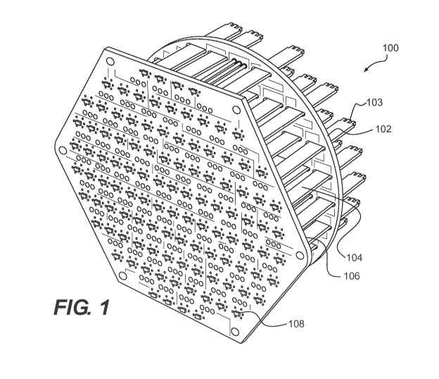
[0027] Figure 1 shows a LED light constructed according to the principles of
the invention. In particular, LED light 100 may include a driver printed
circuit
board (PCB) 102 and a power printed circuit board (PCB) 106, thermal tabs
104 and LED elements 108. This particular arrangement of a LED light 100
provides reduced material costs together with improved cooling of the light as
the heat generated from LED elements 108 may be transferred to thermal
tabs 104 through power PCB 106. The thermal tabs 104 have a thin cross-
section, a great deal of surface area for heat transfer, and use minimal
materials such as aluminum. The thermal tabs 104 are arranged such that air
may flow therearound to cool the LED light 100. Moreover, the tabs 104 may
be arranged as desired to provide selective heat sinking to the LED light 100.
The tabs 104 may be configured with fingers 103 at one or both ends of a tab
104 for insertion into a PCB, such as power PCB 106. This particular
arrangement is also well-suited for automated manufacturing process to be
described below in greater detail. However, other arrangements of these
components providing similar results is contemplated. For example, the tabs
104, power PCB 106, and driver PCB 102 may have any shape or
configuration. Further, although the description of the invention herein is
directed to LEDs, other light generating device types benefit from the same
process described herein.
6
CA 02737046 2011-03-11
WO 2010/030786 PCT/US2009/056520
[0028] Figures 2-14 show process steps that are contemplated to be used
together. However, the invention is further contemplated to use other
additional steps or fewer steps as described below.
[0029] Figure 2 shows a step of a process performed according to the
principles of the invention. As shown in Figure 2, one step may be to form the
driver PCB 102 by forming openings or slots 202 for the thermal tabs 104.
These openings 202 may be formed by routing the driver PCB 102 or the like.
The slots may be formed with a cross section dimension that is about 10%%E3 -
15% larger than the thermal tab 104. Additionally, holes may be formed in the
driver PCB 102 for insertion of two or more thermal tabs 104 that are
dedicated for providing power to the driver PCB 102. For example, in the
embodiment shown in Figure 2, there may be at least one, preferably two or
more insertion points for the power pens or tabs that may be used to provide
power transfer to and within the device. Additionally, around the power tab
opening 203 there may also be about 15 rails of exposed ring around the tab
slot for solder. There may be one or more power tab openings 203, denoted
by 1-N.
[0030] Figures 3A and 3B show another possible step of the process
performed according to the principles of the invention. Figure 3A is an
expanded view of a driver PCB 102. In order to manufacture this particular
arrangement of the driver PCB 102 or any similar arrangement that is
contemplated by the invention, the driver PCB 102 may be formed with a
group of others in a palletized arrangement 302 as shown in Figure 3B. This
type of arrangement may improve the automated manufacturing of the LED
light 100. Additionally, the palletized arrangement 302 shown in Figure 3 may
include one or more alignment holes 304. The alignment holes 304 may help
7
CA 02737046 2011-03-11
WO 2010/030786 PCT/US2009/056520
to ensure alignment with the below described palletized power PCB 106. The
alignment holes 304 should be formed in a plurality to ensure a proper
sustained alignment during the manufacturing process.
[0031] Figure 4 shows another possible step of the process performed
according to the principles of the invention. Referring to Figure 4, the
arrangement of the power PCB 106 is shown. In particular, the power PCB
106 may be formed from 62 mil 4 oz. copper, however other sizes may be
employed. Included in the power PCB 106 may be a plurality of insertion
points 404 for the thermal tabs 1Ã04. In the configuration shown in Figure 4,
the thermal tabs 104 may have on one or both ends a series of one or more
fingers 103 (Fig. 1 and/or Fig. 7). Accordingly, in the embodiment shown in
Figure 4, each thermal tab 104 may have three fingers and the power PCB
106 may have a corresponding number of holes for each thermal tab 104 to
be inserted into. Other hole or slot arrangements are possible and
contemplated by the invention herein.
[0032] Figures 5A and 5B show another possible step of the process
performed according to the principles of the invention. Figure 5A is an
expanded view of a power PCB 106. Figure 5B shows the palletized
arrangement that may be used with the palletized arrangement of the power
PCB 106 configuration, such as shown in Figure 1, or any other contemplated
PCB. In particular, multiple power PCBs 106 may be arranged on a single
palletized structure 502 that may include reference holes 504 that may be
aligned with the reference holes 304 of the driver PCB pallet 302. Again this
palletized arrangement and configuration together with the alignment holes
may provide increased automation capabilities along with increased quality of
the final product.
8
CA 02737046 2011-03-11
WO 2010/030786 PCT/US2009/056520
[0033] Figures 6A and 6B show another possible step of the process
performed according to the principles of the invention. Figure 6A shows an
expanded view of a driver PCB 102 with a power PCB 106, while Figure 6B
shows the alignment of the driver PCB 102 and the power PCB 106 using the
reference holes 504 and 304. In this arrangement of Figure 6B, the thermal
tab insertion points on the power PCB 106 and the driver PCB 102 are
aligned and the thermal tabs 104 may be inserted therethrough. In one
aspect, the length of the palletized driver PCB 102 may be larger compared to
the palletized power PCB 106 as shown in Figure 6B in one dimension (i.e.,
width). Moreover the height of the palletized power PCB 106 may be
somewhat larger than the palletized driver PCB 102. This sizing arrangement
has a number of manufacturing benefits described more fully below. During
manufacturing, solder may be dispensed on the palletized driver PCB 102
including the slot rings and components, if any, before the PCB alignment.
[0034] Figures 7A, 7B, 7C show other possible steps of the process
performed according to the principles of the invention. Referring to Figure
7A,
this Figure shows an embodiment of a thermal tab 104. In particular the
thermal tab 104 may include a solder finger 109 and also insertion fingers 103
as described previously. Other solder fingers and insertion fingers
arrangements and designs are contemplated. Shown in Figure B is the
insertion of the thermal tab 104 into the power PCB 106 and the driver PCB
102. In particular, the thermal tab 104 may be inserted into the power PCB
106 where the slots on the driver PCB 102 are configured to be about 10%
15% larger than the cross section of the thermal tab 104. The larger opening
of the slot for the thermal tab 104 may protect the thermal tab from hitting
the
driver PCB 102 while being inserted into the power PCB 106 which may be
9
CA 02737046 2011-03-11
WO 2010/030786 PCT/US2009/056520
positioned on the bottom as shown in Figure 713. Moreover, the thermal tab
104' may be inserted into the driver PCB 102 only, at certain positions where
there is no slot. This allows the thermal tab 104' to electrically connect to
the
driver PCB 102 as shown in Figure 7C. These thermal tabs 104' inserted only
into the driver PCB 102 may be used as a main AC (or DC) power input, or
other use, such as carrying a signal.
[0035] Figure 8 shows another possible step of the process performed
according to the principles of the invention. In particular, Figure 8 shows
the
arrangement of the thermal tabs 104 in both the power PCB 106 and a driver
PCB 102. Again, it should be noted that at least one of the thermal tabs 104
may be used as a main power input (tall center tab 104') as indicated in
Figure 8. This tab may extend above the other thermal tabs as shown.
[0036] Figures 9A, 913, 9C, 90 show other possible steps of the process
performed according to the principles of the invention. Figure 9A shows the
palletized power PCB and palletized driver PCB of Figure 9C on transport
rails in an insertion machine for performing the insertion process as shown in
relation to Figure 9C. Figure 9B shows the palletized power PCB and
palletized driver PCB of Figure 90 on transport rails between an insertion
machine and a pick and pace machine. As further shown in the sequence
from Figure 9C to Figure 90, the driver PCB 102 may be displaced from the
power PCB 106, as will now be explained more fully. As shown in Figure 9C,
both the power PCB 106 and the driver PCB 102 may be located adjacent to
each other on a transport rail 902. But as shown in relation to Figure 9D, the
two PCBs may be separated as the rail 902 is moved outwardly so as to
support only the driver PCB 102. More specifically during the insertion
process of Figure 9C, both the palletized driver PCB 102 and power PCB 106
CA 02737046 2011-03-11
WO 2010/030786 PCT/US2009/056520
may be supported under edges of the power PCB 106. The width of the
insertion conveyor belts or rails 902 may be adjusted to support the power
PCB 106, which May also support the palletized driver PCB 102, as shown in
Figure 9C.
[0037] After finalizing the insertion process of Figure 9C, the driver and
power PCB 102, 106 assemblies may be transported via an inline conveyor
902 into a Surface-Mount Technology ( MT) machine. The width of the inline
and SIFT machine conveyor belts may then be moved or adjusted outwardly
to support only the palletized driver PCB 102 and shown in Figure 9D. At this
point, the palletized power PCB 106 may no longer be supported directly by
the conveyor belts or rails 902. Gravity or any other force may displace the
palletized power PCB 106 shown in Figure 9D. Solder fingers 109 as
described above may limit movement of the Power PCB 106 and thus ensure
proper displacement of the power PCB 106. At this time, the solder fingers
109 may actively be placed on the solder pads. Furthermore, the thermal tab
104' inserted into only driver PCB 102 may not be displaced as shown in
Figure 9D. Again, these thermal tabs 104' may be used as the main power
input, or similar function.
[0038] Figure 10 shows another possible step of the process performed
according to the principles of the invention. In particular, Figure 10 shows
an
exemplary component placement process on the driver PCB 102. In
particular, an STMT machine may include an S MT machine placement head
920. This head May include a vacuum component nozzle 925. The vacuum
component nozzle 925 may be used to generate a vacuum to hold a
component 930, such as a driver component, to be placed on the driver PCB
102. During this time the STMT machine may be arranged so that it supports
11
CA 02737046 2011-03-11
WO 2010/030786 PCT/US2009/056520
only the palletized driver PCB 102 edges by the rails 902. Additionally the
vacuum component nozzle may be configured such that it is larger than the
height of the power supply thermal tab 104' above the driver PCB 102 to
ensure that the vacuum component nozzle can place the component.
[0039] Figures 11A and 11 B show other possible steps of the process
performed according to the principles of the invention. More specifically,
Figures 11 A and 11 B show a first reflow process. In particular, an oven
conveyor or rail 902 may be supporting the driver PCB 102. As shown in
Figure 11A, a hot air flow step may be directed during the first reflow
process
to allow the solder to reflow on the driver PCB surface 102. In the step of
Figure 11 B, a cooling process is shown where a cold air flow may be directed
at the driver PCB 102 and the power PCB 106 to cool both structures.
[0040] Figures 12A, 12B and 12C show other possible steps of the process
performed according to the principles of the invention. In particular, Figures
12A, 12B and 12C show the 180 degree flip (see Figs. 12B and 12C) and 90
degree rotation (see Fig. 12A) of the palletized assembly. In particular,
during
these steps of the manufacturing process, the assembly may be supported
only under the edges of a palletized driver PCB board 102, as shown in Fig.
12B. In the flip station, the assembly may be flipped 180 degrees as shown
from Fig. 12B to Fig. 12C. At the same time in the flip station, the assembly
may also be rotated 90 degrees, as shown in relation to Fig. 12,,x. Now the
edges of the palletized power PCB 106 extend side to side and the assembly
(combined power PCB 106 and driver PCB 102) may be conveyed on those
power PCB 106 edges due to the above described dimensions.
[0041] Figure 13 shows another possible step of the process performed
according to the principles of the invention. More specifically, Figure 13 now
12
CA 02737046 2011-03-11
WO 2010/030786 PCT/US2009/056520
shows the use of a S 11T machine together with an STMT machine placement
head 920 with a vacuum component nozzle 925 to attach LEDs 931 to the
power PCB board 106. In particular, the SIFT machine supports the palletized
power PCB 106 edges and, in this regard, the LEDs are placed on the pads
with previously dispensed solder.
[0042] Figures 14A and 14B shows still other possible steps of the process
performed according to the principles of the invention. As shown in Figures
14A and 14B, a second reflow process may be perforrmed. In particular, a hot
air flow step during the second reflow process may be directed both to the top
of the assembly and bottom of the assembly as shown in Figure 14A. The
temperature of the hot air flow to the bottom of the assembly may be adjusted
not to exceed a reflow temperature of the solder used. Moreover, the
temperature of the hot air flow to the top of the assembly which is the LED
side, should be slightly below the recommended lead free reflow temperature.
Thereafter, as shown in relation to Figure 14B, a step of directing cod air
may
be performed to cool the entire assembly. The temperature of the cold air to
the bottom of the assembly during the cooling process may be at least 40%
lower compared to the top flow to provide improved results.
[0043] Figure 15 shows an exemplary implementation of a light according
to the principles of the invention. In particular, Figure 15 shows the LED
light
100 held in a housing 1502. The housing may include a standard screw type
electrical connection 1504. Other types of connections for other light
arrangements are contemplated. The housing 1502 may also include an
open, slotted, or fin type construction 1506 that allows air flow to the back
of
the LED light 100, and in particular, the thermal tabs 104. The housing 1502
may be formed of any material including synthetic materials such as plastic.
13
CA 02737046 2011-03-11
WO 2010/030786 PCT/US2009/056520
[0044] Although the lights of the invention are well-suited as light sources
for homes and businesses such as shown in Figure 15, the invention is also
well-suited as light sources for computer monitors, TVs, and the like, as well
as other applications.
[0045] Accordingly, the invention as described above provides a
manufacturing process for LED lights that uses a reduced amount of
materials, has an arrangement that can be more easily manufactured in an
automated fashion and that furthermore includes other advantages. In
particular, this arrangement results in selective heat sinking, no or fewer
wires, no or fewer mechanical fasteners, no or less thermal grease, no or
limited use of metal PCBs, no or limited hand soldering, use of heat sink
components to provide power, no or fewer capacitors, and small or multiple
dies. This particular arrangement is also well-suited for an automated
manufacturing process. However, other arrangements of these components
providing similar results is contemplated. Further, although the description
of
the invention herein is directed to LEDs, other light generating types benefit
from one or more process steps described herein.
[0046] While the invention has been described in terms of exemplary
embodiments, those skilled in the art will recognize that the invention can be
practiced with modifications in the spirit and scope of the appended claims.
These examples given above are merely illustrative and are not meant to be
an exhaustive list of all possible designs, embodiments, applications or
modifications of the invention.
14