Note: Descriptions are shown in the official language in which they were submitted.
CA 02737260 2011-03-14
WO 2010/036208 PCT/SG2009/000329
- 1 -
SOLAR ELECTRIC PANEL
Field of the Invention
The present invention relates to a solar electric panel
particularly, though not exclusively, for use on a roof of
a building to provide electrical energy for the building.
Background of the Invention
It is well known to use solar electric panels to provide
power to electrical apparatus or storage devices.
Depending on the specific application at hand, the panels
may be either free-standing or applied to a roof of a
building. When the panels are applied to a roof of a
building, they may typically overlie an existing roof
covering.
Applicant has previously devised a photovoltaic tile*
assembly for converting solar energy to electricity. The
photovoltaic tile assembly is configured in a manner so
that it can also act as a roof covering and thereby be
used in place of traditional roof coverings such as tiles,
slate and iron.
Further details of Applicant's above-described
photovoltaic tile assembly are provided in Singapore
patent application No. 200716871-9.
Summary of the Invention
In one aspect, the present invention provides a solar
electric panel comprising:
a base tile;
a plurality of photovoltaic tiles, each photovoltaic
tile comprising one or more photovoltaic cells
CA 02737260 2011-03-14
WO 2010/036208 PCT/SG2009/000329
2 -
electrically connected together to form a photovoltaic
cell circuit;
a connection system supported on or in the base tile,
.the connection system electrically connecting the
photovoltaic tiles together in groups of two or more
photovoltaic tiles, and mechanically coupling the
photovoltaic tiles to the base tile, the connection system
being configured to facilitate electrical coupling of the
base tile with an adjacent base tile; and
at least one bypass device shunted across a set of
one or more of the photovoltaic cells in the photovoltaic
cell circuit, wherein the bypass device provides a current
path for the photovoltaic cell circuit across the set of
photovoltaic cells when an output voltage across the set
of photovoltaic cells is less than a predetermined
threshold voltage.
The connection system may comprise:
a plurality of conducting posts, each post having a free
end to which the photovoltaic tiles are coupled; and,
a plurality of electrical conductors that electrically
connect the posts together.
The connection system may comprise a first electrical
connector and a complementary second electrical connector
wherein the first electrical connector is coupled to an
end of the electrical conductor connected to a first of
the posts and the second electrical connector is coupled
to an end of the electrical conductor connected to a last
of the posts whereby the first electrical connector of one
electrical connection system can be electrically connected
with a second electrical connector of a second electrical
connection system to provide electrical continuity
between the first and second electrical connection
systems.
One or both of the first and second electrical connectors
CA 02737260 2011-03-14
WO 2010/036208 PCT/SG2009/000329
3 -
may be provided with a degree of resilience so as to apply
a mechanical force between first and second electrical
connectors when coupled together, the mechanical force
acting to maintain coupling between the first and second
electrical connectors.
The first and second electrical connectors may also be
configured to form, when engaged with each other, a mutual
contact surface of variable length.
The free end of each post may be provided with a fitting
to enable mechanical and electrical connection to the
photovoltaic tile.
The fitting may comprise a plurality of resilient, or
resiliently supported, radially extending projections,
formed about the free end of the post.
In an alternate embodiment the fitting may comprise a
combination of_ (a) a screw thread formed on the free end
of the post and a nut adapted to be screwed onto the
thread, or (b) a screw thread formed in the free end of
the post and a screw or bolt adapted to be screwed onto
the thread.
In one embodiment of the solar panel the electrical
conductors and posts are encapsulated to form an
electrical connection tile, wherein the free end of each
post is accessible to facilitate connection with the
photovoltaic tiles.
In one form of the connection system each electrical
conductor comprises a conducting rail to which a plurality
of the posts is connected.
However in an alternate form of the connection system each
electrical conductor comprises one or more wires, or one
CA 02737260 2011-03-14
WO 2010/036208 PCT/SG2009/000329
- 4 -
or more conducting tracks on a circuit board. In this
form, the wires or tracks are configured to enable custom
connection to the posts to provide selectable connection
configurations. For example the wires or tracks may be
configured to provide a series connection between the one
or more first electrical devices or apparatuses.
The base tile may be made from a moldable material and the
connection system is molded into the substrate.
In an alternate embodiment the base tile comprises a
bottom shell defining a cavity in which the connection
system is disposed. In this embodiment the base tile
comprises a top shell which overlies the cavity and is
provided with a plurality of holes in alignment with the
posts wherein the posts extend toward corresponding holes.
The base tile may comprise a plurality of markers on a
first surface-each marker positioned at a location whereby
a'mechanical fastener passing through a marker in a plane
perpendicular to a plane containing the base tile is
spaced from the connection system.
The base tile may also comprise a sealing system for
providing a waterproof seal between adjacent abutting base
tiles.
Each photovoltaic tile may comprise:
a carrier tile having a first side; and
a cover plate sealed to the carrier tile, the cover plate
having a first side, wherein the carrier tile and the
cover plate are relatively configured to form a recess
therebetween when cover plate overlies the carrier tile
with the respective first sides facing each other, wherein
the one or more photovoltaic cells are seated in the
recess.
CA 02737260 2011-03-14
WO 2010/036208 PCT/SG2009/000329
-
In one form of the panel, the photovoltaic tile, when
viewed from a side provided with the cover plate may have
a slate-like appearance.
5 In addition the carrier tile may be of a slate-like
colour.
The photovoltaic cells may also be of a slate-like colour.
The cover plate may have substantially the same footprint
as the carrier tiles so that respective edges of the
carrier tile and cover plate are substantially co-
terminus.
In one embodiment the recess may be formed in the first
surface of the carrier tile. In this embodiment the cover
plate can be seated in the recess.
The photovoltaic tiles may comprise one or more through
hole electrical terminals by which the photovoltaic tiles
are electrically and mechanically coupled by the
connection system.
The photovoltaic tiles may further comprise electrical
cell conductors providing an electrical connection between
each electrical terminal and the one or more photovoltaic
cells.
The electrical cell conductor may be molded into the
carrier tile for at least a portion of their length
extending from the terminals.
Each bypass device comprises a switching device.
At least one of the bypass devices may be a diode.
At least of the one diodes is selected to have a forward
voltage drop of equal to or less than 0.7 V.
CA 02737260 2011-03-14
WO 2010/036208 PCT/SG2009/000329
6 -
In one form of the panel, at least one switching device is
an anti-fuse or a transistor switching device.
At least one diode may be shunted across one or more of
the photovoltaic cells in a manner such that each
diode is reverse biased by the one or more
photovoltaic cells across which it is shunted.
The at least one bypass device may be thermally insulated
so as to reduce leakage current therefrom.
Brief description of the Drawings
Figure 1 is a partial exploded view from the top of a
solar electric panel in accordance with a first embodiment
of the present invention;
Figure 2 is an exploded view from the bottom of a base
tile incorporated in the solar electric panel shown in
Figure 1;
Figure 3 depicts a method of attaching the solar electric
panel to a supporting structure;
Figure 4 is a view of section AA of the base tile shown in
Figure 2;
Figure 5 is a pan view of two base tiles.side by side;
Figure 6 is an isometric view of a corner of a two base
tiles prior to joining to each other;
Figure 7 is a cross section view of two base tiles
connected to a supporting structure;
Figure 8 is a side view of solar electric panel;
CA 02737260 2011-03-14
WO 2010/036208 PCT/SG2009/000329
7 -
Figure 9 is an enlarged isometric view of a corner of the
solar electric panel;
Figure 10 is a representation of one form of connection
system incorporated in the solar electric panel when
electrically connecting two solar electric panels
together;
Figure 1.1 is a further representation of the connection
system;
Figure 12 is an enlarged view of one form of fitting of
the connection system to mechanically couple a
photovoltaic tile of the solar electric panel to a base
tile;
Figure 13 is an equivalent circuit diagram of the
connection system shown in Figures 10 and 11;
Figure 14 is an enlarged view of a second form of fitting
of the connection system to mechanically couple a
photovoltaic tile of the solar electric panel to a base
tile;
Figure 15 is an enlarged view of a third form of fitting
of the connection system to mechanically couple a
photovoltaic tile of the solar electric panel to a base
tile;
Figure 16 is depicts an alternate form of base tile and
connection system incorporating a forth form of fitting to
mechanically couple a photovoltaic tile of the solar
electric panel to a base tile;
Figure 17 is an exploded view of the base tile and
connection system shown in Figure 16;
CA 02737260 2011-03-14
WO 2010/036208 PCT/SG2009/000329
8 -
Figure 18 is an equivalent circuit diagram of the
connection system shown in Figures 16 and 17;
Figure 19a is a representation of one form of photovoltaic
tile incorporated in the solar electric panel;
Figure 19b is an exploded view of the photovoltaic tile
shown in Figure 19a;
Figure 19c is a schematic representation of a carrier tile
incorporated in the photovoltaic tile depicted in Figures
19a and 19b;
Figure 20a is a representation of a second form of
photovoltaic tile incorporated in the solar electric
panel;
Figure 20b is an exploded view of the tile shown in Figure
20a;
Figure 20c is a schematic representation of a carrier tile
incorporated in the photovoltaic tile depicted in Figures
20a and 20b;
Figure 21 is a representation of a portion of a roof
covered by a plurality of solar electric panels;
Figure 22 is a cross section of one form of sealing system
incorporated in the photovoltaic tile;
Figure 23 is a cross section of a second form of sealing
system incorporating in the photovoltaic tile;
Figure 24 shows a perspective view of a photovoltaic tile
having a photovoltaic cell circuit composed of a 3x3
matrix of series connected photovoltaic cells;
CA 02737260 2011-03-14
WO 2010/036208 PCT/SG2009/000329
9 -
Figure 25 shows a graph of the open circuit voltage of the
photovoltaic cell circuit of Figure 24 as a function of
the number of photovoltaic cells that are shaded from
impinging light;
Figure 26 shows a circuit diagram of the photovoltaic cell
circuit of Figure 24 incorporated in a test circuit;
Figure 27 shows a bypass device shunted across one
photovoltaic cell of the photovoltaic cell;
Figure 28 shows a circuit diagram of the photovoltaic cell
circuit of Figure 27 having the shunted photovoltaic cell
shaded from impinging light;
Figure 29 shows a bypass device shunted across all of the
photovoltaic cells of the photovoltaic cell; and
Figure 30 is a circuit diagram showing a series connection
of two shunted photovoltaic cell circuits of the type
shown in Figure 29.
Description of Embodiments
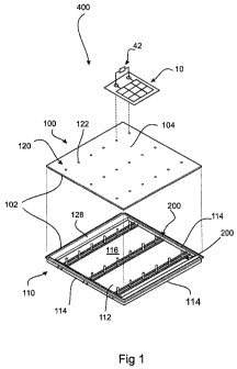
Figure 1 is a schematic representation of an embodiment of
a solar panel 400. The solar panel 400 comprises: a base
tile 100, a plurality of photovoltaic tiles 10 (only one
shown in this Figure), a connection system 200, for each
photovoltaic tile 10 one or more electrical bypass devices
42. More particularly each photovoltaic tile 10 comprises
one or more photovoltaic cells 12 electrically connected
together to form a photovoltaic cell circuit 40. The
connection system 200 is supported by or on the base tile
CA 02737260 2011-03-14
WO 2010/036208 PCT/SG2009/000329
- 10 -
100, and electrically connects the photovoltaic tiles 10
together in groups of two or more photovoltaic tiles, and
mechanically couples the photovoltaic tiles 10 to the base
tile 100. In addition the connection system is configured
to facilitate electrical coupling of the base tile 100
with an adjacent base tile. At least one bypass device 42
is shunted across a set of one or more of the photovoltaic
cells 12 in the photovoltaic cell circuit 40. Each bypass
device 42 provides a current path for the photovoltaic
cell circuit 40 across the set of photovoltaic cells 12
when an output voltage across the set of photovoltaic
cells is less than a predetermined threshold voltage. As
explained in greater below this reduces voltage drop the
solar panel 400 in the event the voltage output an
individual cell 12 is reduced so as to act as a high
impedance or effective short circuit, which may arise for
example due to the shadow effect.
The panel 400 may be connected to a plurality of adjacent
panels 400 to provide increased electrical output. The
panel 400 may be deployed in say an array supported by a
ground based frame. Alternately the panel may be mounted
on a roof of a building and connected to an electrical
power management system to provide power to electrical
devices in the building.
Various components of the photovoltaic tile will now be
described in greater detail.
Base Tile 100
With reference to Figures 1-9, one possible form of the
base tile 100 comprises a substrate 102 having which
supports or holds the electrical connection system 200.
While the connection system 200 is described in greater
detail later, a brief description is provided now to aid
in the understanding of the structure and function of the
CA 02737260 2011-03-14
WO 2010/036208 PCT/SG2009/000329
- 11 -
base tile 100. The connection system 200 comprises a
plurality of electrically conducting posts 204 connected
together by electrical conductors 202. Each post 204 has a
free end 206 that can be accessed from or extends beyond a
first surface 104 of the substrate 102. This enables and
facilitates both electrical connection of the photovoltaic
tiles 10 together and mechanical coupling of the
photovoltaic tiles 10 to the base tile 100.
In this embodiment the substrate 102 comprises a bottom
shell 110 having a planar bottom surface 112, and a
peripheral wall 114 extending about the bottom surface
112. The bottom surface 112 and the peripheral wall 114
define a cavity 116 in which the conductors 202 are
disposed.
Optionally, the cavity 116 may be filled with an
insulating material to provide thermal insulation through
the base tile assembly 110.
When the substrate 102 is formed with the bottom shell
110, it may also be provided with a top shell 120 that
overlies the cavity 116 and is provided with a plurality
of holes 122 through which the free ends 206 of the posts
204 extend. The surface of the top shell 120 opposite the
cavity 116 forms the first surface 104 of the base tile
100. Top shell 120 is sealed to the bottom shell 110 to
prevent the ingress of water into the cavity 116. This
may be achieved by the use of mechanical seals, sealants,
adhesives, or ultrasonic welding. Use of ultrasonic
welding is particularly suitable when the substrate 102 is
made from a plastics material.
In order to provide a degree of compression resistance to
the base tile 100, a surface 124 of the top shell 120
which faces the cavity 116 is provided with a plurality of
depending legs or struts 126 (see Figures 2 and 4). The
CA 02737260 2011-03-14
WO 2010/036208 PCT/SG2009/000329
- 12 -
legs 126 bear against the bottom surface 112 when the top
shell 120 is attached to the bottom shell 110.
The bottom shell 110 is provided with two solid benches or
strips 128 that extend on the inside of the cavity 116
parallel to each other and on opposite sides of the shell
110. When the solar panel 400 is used as in a roof based
energy system, the base tile 100 may be fixed to rafters
348 of the roof by mechanical fasteners such as nails or
screws 130 that are driven through the thickened strips
128. In order to ensure a user drives the nails or screws
130 through the strips 128 and therefore avoids the
electrical connection system 200, the top shell 120 is
provided with four markers 132, one in each corner. The
markers 132 may be in the form of: a simple indelible mark
made on the first surface 104; indentations; or, through
holes.
Base tile 100 is provided with a tile sealing system 134
for providing a waterproof seal between adjacent abutting
base tiles 100. With particular reference to Figures 4-7,
the tile sealing system 134 in this embodiment comprises
laterally extending tongues 136 that run along two
adjacent sides of the base tile 100 and to longitudinal
grooves 138 that run along the two remaining sides of the
base tile 100. The tongues 136 are formed integrally with
the bottom shell 110 as shown most clearly in Figures 4
and 7. Rubber sealing strips 140 are partially embedded
in, and on opposite sides of, each tongue 136. Each
groove 138 is formed as a space between the bottom shell
110 and the top shell 120. More particularly, with
reference to Figure 4, it can be seen that the groove 138
is formed as the combination of a rebate 142 formed in one
of the peripheral walls 114 and an overhanging portion 144
of the top shell 120. When the tongue 136 of one base
tile assembly is inserted into the groove 138 of an
adjacent tile assembly a waterproof seal is formed between
CA 02737260 2011-03-14
WO 2010/036208 PCT/SG2009/000329
- 13 -
the respective adjacent base tiles 100.
The substrate 102 and more particularly the bottom shell
110 is provided with a plurality of holes 146 along
opposite peripheral walls 114 to allow electrical
connection between the electrical conductors 202 when
adjacent base tiles 100 are coupled together. Figures 8
and 9 depict the holes 146 formed in the peripheral wall
114 containing the groove 138. Ends of the conductors 202
extend through the holes 146. Corresponding holes are
formed in the peripheral wall 114 on the opposite side of
the bottom shell 110 which are in alignment with the holes
146 on an adjacent base tile. Thus when two base tiles
100 are coupled together, the connection system 200 in
each tile 100 are also electrically coupled together.
Connection System 200
Figures 10-12 depict one form of the connection system 200
where the electrical conductors are in the form of rails
202 to which a plurality of electrically conducting posts
204 is connected. In this embodiment, each rail 202 is in
the general form of a square section metallic tube or rod.
The posts 204 extend parallel to each other and
perpendicular to the rail 202. Each post 204 is coupled
to the rail 202 by a short transverse link 205. In one
embodiment, the posts 204 may be welded, brazed or
soldered to the links 205 which may be formed integrally
with the rail 202. Alternatively the links 205 may be
formed separately and subsequently attached to the rail
202. In a further variation it is possible for the posts
204 to be provided with a detachable coupling for
connecting to the links 205. In yet a further variation
the rail 202 and posts 204 may be integrally formed.
A male connector 208 and female connector 210 at opposite
ends of the rail 202 constitute one form of complementary
CA 02737260 2011-03-14
WO 2010/036208 PCT/SG2009/000329
- 14 -
connectors that may be utilized in the connection system
200 to enable electrical connection between adjacent rails
202. In this embodiment, the male connector 208 is in the
form of two spring arms 212 formed at one end of a rail
202, while the female connector 210 is in the form of a
simple hole 214 at the opposite end of the rail 202. The
spring arms 212 and the hole 214 are relatively configured
so that when the spring arms 212 are inserted into the
hole 214 they provide a degree of resilience to apply a
mechanical bias force. This acts to provide both
mechanical and electrical coupling between adjacent rails
202.
Numerous different types of configuration of electrical
connectors may be provided at the opposite ends of each
conductor (rail) 202. For example, the spring arms 212
may be replaced with a banana plug type connector.
Alternatively, the connector 208 may be provided with one
or more sprung contact balls which contact the inside
surface of the hole 214. Indeed, the inside surface of
the hole 214 may also be provided with complementary
shaped recesses for receiving corresponding sprung balls.
This will provide a snap-type fitting.
In the connection system 200 shown Figures 1, 4 and 10 the
rails 202 are arranged in pairs. This enables respective
rails in the pair to act as a nominal positive rail and a
nominal negative rail. Further, as shown in the above
mentioned figures together with Figure 3, the rails 202 in
each pair are arranged so that their respective posts 204
are alternatively disposed in a direction parallel to the
rails 202, and more particularly are in mutual alignment.
For example with reference to Figure 3, which shows the
free ends 206 of post 204 extending above the surface 104
of a base tile 100, each second free end 206a in a bottom
row 201 is connected to the same rail 202, with each
interleaving pair of post 206b coupled to the other rail
CA 02737260 2011-03-14
WO 2010/036208 PCT/SG2009/000329
- 15 -
in the rail pair. Thus when a photovoltaic tile 10 is
mounted on a base tile 100 the terminals 28 and 30 of the
tile 10 are electrically coupled with posts 204 of
different rails 202 in a rail pair.
Figure 13 (ignoring the phantom connections 260 for the
time being) shows an equivalent circuit of the connection
system 200 where the photovoltaic tiles 10 are modeled as
4.5v voltage sources 10m. The rails 202 of each pair
provide a parallel connection for the connected tiles 10.
Thus one base tile 100 will provide three independent
"banks" of parallel connected tiles 10. The pairs of rails
in one base tile connect to corresponding pairs of rails
on adjacent base tiles 100. This provides an extended
parallel connection of the tiles 10 along the base tiles
100. However in a minor variation the connection system
may be modified to provide a series connection between the
three pairs of rails in each base tile 100 thus providing
a series connection of three banks of parallel connected
tiles 10 (which is equivalent to all of the tiles 10 being
connected together in parallel with each other on one and
the same base tile 100). This is depicted by the phantom
connections 260 in Figure 13.
In the connection system 200 and as shown in Figures 4, 6,
8, and 10-12 the free end 206 of each post 204 extends
above the first surface 104 of the base tile 100. The free
end 206 is provided with a fitting 216 to enable
electrical connection and mechanical coupling of a
photovoltaic tile 10. The photovoltaic tile 10 is
provided with through hole terminals 28 and 30. The
construction of the photovoltaic tile 10 is described in
greater detail later.
Four different forms of fitting 216 are described in this
specification, however those skilled in the art will
appreciate that any other specific construction of fitting
CA 02737260 2011-03-14
WO 2010/036208 PCT/SG2009/000329
- 16 -
216 that performs the same function as the embodiments
described hereinafter can of course be used with other
embodiments the present invention.
One form of fitting 216a which comprises a plurality of
resilient or resiliently supported radially extending
projections in the form of fins or barbs 218 is shown in
Figures 4, 6 and 10-12. Here, four fins 218 are shown
evenly disposed about the free end 206 of the post 202.
Each fin is formed with a rounded upper shoulder 220 and
is spring biased outward of the post 204. That is, the
fins 218 can be moved in a radial inward direction against
the spring bias to allow the free end 206 to pass through,
for example, the through hole terminal 28. Once the free
end 206 is passed through the connector 28, the fins 218
extend radially outward by action of a spring and their
lower surface bears on and thus make electrical contact
with the terminal 28.
The fins 218 also provide mechanical coupling to retain
the photovoltaic tile 10 on the base tile 100. In order
to mechanically separate the photovoltaic tile 10 from the
post 204, the fins 218 must be pushed radially inward
against the spring to an extent that collectively they
circumscribe a circle having a diameter smaller than an
inner diameter of the terminal.
A resilient cap 222 is fitted to the top of the free end
206 to provide a degree of cushioning to an overlying
photovoltaic tile 10.
Figure 14 depicts a second form of fitting 216b which
comprises the combination of a screw thread 224 formed
about the free end 206 of a post 204, and a threaded cap
226 that can be screwed onto the thread 224. The cap 226
is made from an electrically conducting material. In one
variation, in order to minimize the risk of the ingress of
CA 02737260 2011-03-14
WO 2010/036208 PCT/SG2009/000329
- 17 -
water and possible corrosion to both the fitting 216b and
the terminal 28, the nut 226 may be formed with a blind
hole rather than a through hole.
In a further variation or modification, the nut 226 may be
embedded or carried by a cap 228. In one form, the cap
228 may be formed of a transparent or translucent plastics
material. This may assist installers in lining up the nut
226 with the post 204. A waterproof seal in the form of
an 0-ring may also be embedded in a bottom surface of the
cap 228, to form a seal against the terminal 28 to prevent
the ingress of water and thus minimize the risk of
corrosion of the terminal 28 and the fitting 216b.
Alternatively, the entire cap 228 may be formed of a
resilient material.
Figure 15 depicts a further variation of the fitting 216c.
In this embodiment, the fitting 216c comprises the
combination of a radially extending spring 230 which
extends from opposite sides of the free end 206, and a
pair of electrically conducting fingers 232 spaced above
the spring 230. The fingers 232 are resiliently supported
so that they may be sprung radially inward to enable them
to pass through the through hole terminal 28. Thus in
order to couple a photovoltaic tile 10 to a post 204
provided with a fitting 216c, the fingers 232 are sprung
inwardly as the photovoltaic tile 10 is pushed onto the
free end 206. The spring 230 is deflected downwardly
during this process. When the tile 10 has been pushed
down so that the fingers 232 are now clear of the terminal
28, they release to spring outwardly to an extent beyond
the internal diameter of the terminal 28. The spring 230
applies a bias on the underside of the photovoltaic tile
10 to thereby assist in maintaining electrical contact
between the fingers 232 and the terminal 28.
CA 02737260 2011-03-14
WO 2010/036208 PCT/SG2009/000329
- 18 -
Figures 16, 17 and 18 depict an alternative form for
fitting 216d and corresponding alternate form of base tile
100a and connection system 200a. The fitting 216d
comprises a threaded bore 250 provided axially in each
post 204a and a corresponding threaded screw or bolt 252
having a shank that passes through the electrical
terminals 28 and 30 of a photovoltaic tile 10. The fitting
216d thus provide electrical connection between the
photovoltaic tile 10 and the connection system 200a, while
also mechanically securing the tile 10 the base tile 100a.
In this form of the connection system 200a the electrical
conductors are in the form of wires 202a rather than rails
202. The use of wires 202a enables electrical connection
of the posts 204a in a customized manner to provide a
desired electrical connection configuration. For example
as shown in Figures 17 and 18 a series connection of all
photovoltaic tiles 10 (modeled as voltage sources 10m in
Figure 18) can be achieved to provide greater output
voltage. The wires may be connected to the posts by
soldering or brazing. When this form of the electrical
connection system is used with the base tile 100a, a
plurality of bosses 113.may be formed on and extending
upward from an inside surface of the bottom shell 110a
into which the posts can be press or interference fit.
The press or interference fit can also provide an
alternate connection mechanism, where the wire is in
effect clamped between the boss and post to provide an
electrical connection. If desired the cavity 116 can be
filled with an encapsulating resin.
In a variation to the embodiment where the conductors are
in the form of wires, the wires and posts may be pre-
connected to provide the desired circuit configuration,
with the posts held in the required position to enable
connection to the photovoltaic tiles 10, then encapsulated
to form an electrical connection tile that can be dropped
CA 02737260 2011-03-14
WO 2010/036208 PCT/SG2009/000329
- 19 -
into the cavity 116. As an alternative to encapsulating,
the base tile could be molded about the pre-connected
wires 202a and posts 204a to form an integrated tile and
connection system.
In yet a further alternative the electrical conductor can
be in the form of one or more conductive tracks formed on
a circuit board, with the posts subsequently soldered or
brazed to the circuit board. The board can then be dropped
into the cavity 116. Prior to doing this the entire board
can be encapsulated for example in a resin/epoxy to form
an electrical connection tile that can provide thermal
insulation for the base tile 100a. When the posts 204a are
used in conjunction with the fittings 216d the posts can
be made of a length to extend between the inside surface
of the bottom shell 110 and the inside surface of the top
shell 120. In this way the posts can also provide
mechanical strength to the base tile 100.
When the electrical conductors are in the form of wires or
tracks on a circuit board complimentary electrical
connectors identical or similar to the male and female
connectors 208 and 210 may be attached to opposite ends of
the circuit formed by the connected wires or tracks to
facilitate electrical connection between connection
systems of adjacent panels 400.
While the posts 204 are described and illustrated as
extending perpendicular to its corresponding rail 202 this
need not be the case. For example, the posts 204 may
extend diagonally of, or in the same plane as, the rails
202. Additionally, there is no requirement for the posts
204 of a rail to extend in the same direction to each
other (i.e., to be parallel). For example if desired
alternating posts 204 attached to the same rail 202 may
extend in different directions. Further, the posts 204 may
be provided on both sides of the rail 202.
CA 02737260 2011-03-14
WO 2010/036208 PCT/SG2009/000329
- 20 -
Photovoltaic Tiles 10
Figures 19a-19c, depict one form of the photovoltaic tile
10 that may be used in the solar electric panel 400. The
tile 10 comprises a carrier tile 12 and one or more
photovoltaic cells 14. The carrier tile 12 has a first
side 18 on which a recess 20 is formed. The photovoltaic
cells 14 are formed a single unit which is dimensioned
relative to the recess 20 to seat in the recess 20. A
cover plate 16 overlies the photovoltaic cells 14 and can
be sealed to the carrier tile 12. In this particular
embodiment the cover plate 16 has substantially the same
footprint as the carrier tile 12, and is juxtaposed so
that the edges of the plate 16 and the tile 12 are co-
terminus.
A front or exposed face 22 of the photovoltaic tile 10 is
provided with a flat surface 24. The formation of the
flat surface 24 is achieved by forming the thickness of
the photovoltaic cell 14 to be substantially the same as
or less than a depth of the recess 20, and providing the
cover plate 16 with a flat upper surface.
When the solar electric panels 400 are used as a roof
covering on a house or other building the photovoltaic
tile 10 can be made to have a slate-like appearance, i.e.,
a slate-like colour to blend in with surrounding houses
and buildings that may be provided with slate or shingle
roofs. This may be achieved by forming the carrier tile
12 of a slate-like colour. Additionally, the photovoltaic
cell 14 can be formed to be substantially clear so that
the slate-like colour of the underlying carrier tile 12 is
visible through the photovoltaic cell 14; or, by forming
the photovoltaic cell 14 to also be of a slate-like
colour. The cover plate 16 is made of a transparent
material to maximize transmission of solar energy to the
CA 02737260 2011-03-14
WO 2010/036208 PCT/SG2009/000329
- 21 -
cell 14. This also enables the slate-like colour of the
underlying carrier tile 12 and/or photovoltaic cell 14 is
visible therethrough.
Edges of the cover plate 16 may be sealed to a peripheral
edge of the carrier tile 12 by use of sealants, adhesives,
or ultrasonic welding.
A lower edge or strip 26 of the photovoltaic tile 10 which
consists of the lower edge of the cover plate 16 is formed
with a curved or rounded cross-section. It is believed
that this may assist in reducing uplift or the effect of
uplift in windy conditions.
In order to collect or otherwise use electricity generated
by the photovoltaic cell 14, the photovoltaic tile 10 is
provided with electrical terminals 28 and 30. The
terminals 28 and 30 are electrically coupled with
electrical contacts 32 and 34 of the photovoltaic tile 14
by respective conductors or bus bars 36 and 38. Each
terminal 28 and 30 is in the form of a ring terminal which
circumscribes respective holes 40 and 42 formed in the
photovoltaic tile 10. In particular, each hole 40 and 42
is formed in a portion 44 of the carrier tile 12. that does
not contain the recess 20.
The bus bars 36 and 38 are electrically coupled to their
respective terminals 28 and 30 by any suitable means such
as by soldering. During the construction of the
photovoltaic tile 10, the terminals 28 and 30 and the bus
bars 36 and 38 can be attached to the photovoltaic cell
14. Recesses or grooves 20 are formed in the carrier tile
to seat the terminals and bus bars when the a photovoltaic
cell 14 is seated in the recess 20 Thereafter, the cover
plate 16 is placed over the photovoltaic cell 14 and
sealed onto the carrier tile 12. Thus the terminals 28 and
30, and the bus bars 36 and 38 are embedded in the
CA 02737260 2011-03-14
WO 2010/036208 PCT/SG2009/000329
- 22 -
photovoltaic tile 10 by way of being sandwiched between
the cover plate 16 and the carrier tile 12.
Figures 20a-20c illustrates a second embodiment of the
photovoltaic tile denoted as 10B, in which the same
reference numbers are used to denote the same features. As
is apparent from a comparison of with Figures 19a-19c the
two embodiments are very similar and according only the
differences in these embodiments will be described.
In essence the main difference between the embodiments is
that the cover plate 16 in the photovoltaic tile 10B is
smaller and in particular is dimensioned to seat in the
recess 20. As a consequence of this the recess 20 is made
deeper with the combined thickness of the cover plate 16
and the photovoltaic cell 14 being about the same as the
depth of the recess 20. This results in the photovoltaic
tile 10B maintaining the flat upper surface 24 described
above in relation to the photovoltaic tile 10B. Also,
because the cover plate 16 is seated in the recess 20, the
curved of beveled profile of the lower edge 26 of the tile
10B is now provided on the carrier tile 12.
The terminals 28 and 30 and the bus bars 36 and 38 are
embedded in the photovoltaic tile 10B by being embedded
and more particularly molded in the carrier tile 12. For
example, the terminals 28 and 30 and a portion of the
length of their attached bus bars 36 and 38 can be moulded
into the carrier tile 12 during the formation of the
carrier tile 12. However, a distal end of each bus bar
extends into the recess 20 and is left free to enable
connection with the photovoltaic cell 14. The cover plate
16 may also be made of a transparent plastics material.
The operation and use of both embodiments of the
photovoltaic tiles 10 and 10B is identical. According for
the sake of simplicity the operation and use thereof is
CA 02737260 2011-03-14
WO 2010/036208 PCT/SG2009/000329
- 23 -
described hereinafter with reference to the tile 10 only.
Figure 21 illustrates an array of solar electric panels
400 and a corresponding array of photovoltaic tiles 10
overlying and coupled to a roof structure 300 which
comprise a plurality of parallel roof rafters 348. As
previously described, the photovoltaic tiles 10 are
connected to an underlying corresponding base tiles 100
which in turn are fastened to the underlying rafters 348.
Hooks 302 (see fig. 8) similar to conventional slate hooks
can be used if required to further assist in supporting
and holding down the photovoltaic tiles 10.
The photovoltaic tiles 10 are arranged in successive rows
52a-52i, with row 52a being lowermost. Successive rows
are staggered by half a photovoltaic tile 10 width
relative to the underlying row. Further, a higher row
partially overlies an adjacent underlying row. For
example, the photovoltaic tiles 10 in the row 52b overlie
the photovoltaic tiles 10 in the row 52a. More
particularly, the photovoltaic tiles 10 in a higher row
overlie portion 44 of the photovoltaic tiles 10 in an
underlying row. This arrangement of photovoltaic tiles 10
provides the roof structure 46 with a roof covering that
has a geometric appearance of a slate or shingle roof.
This appearance is enhanced by the slate-like appearance
and colouring of the photovoltaic tiles 10.
In their simplest form opposite longitudinal side faces of
the photovoltaic tiles 10 are flat and abut against the
side face of an adjacent tile 10. If waterproof sealing is
required a bead of sealant material can be laid between or
over the abutting surfaces. However in an alternate
embodiment, as shown in Figures 22 and 23 opposite
longitudinal sides 54 and 56 of each photovoltaic tile 10
can be formed with sealing structures or components which
when mutually engaged form a waterproof seal between
CA 02737260 2011-03-14
WO 2010/036208 PCT/SG2009/000329
- 24 -
adjacent photovoltaic tiles 10 in any particular row 52.
That is, the side 56 on one photovoltaic tile 10 can
engage and form a seal with the longitudinal side 54 of an
adjacent photovoltaic tile 10. This may be achieved in
several different ways. For example, Figure 22 depicts a
cross section of a tile 10 through portion 44, where the
side 54 is formed with a longitudinal groove 55 and the
side 56 with a longitudinal and laterally extending tongue
57 that fits into the groove and forms a seal therewith.
In an alternative arrangement shown in figure 23 the side
54 is formed with a laterally extending lip 59 of one half
the thickness of the photovoltaic tile 10 and extending
flush with the surface 24, while the side 54 is provided
with a complementary lip 61 also of half the thickness of
the photovoltaic tile 10 but flush with a bottom surface
of the carrier tile 12 so that the side 56 of one
photovoltaic tile 10 can overlie the side 54 of an
adjacent photovoltaic tile 10 to form a waterproof seal.
The sealing effect in both arrangements may be enhanced by
the provision of one or more rubber seals 63 acting
between the tongue 57 and groove 59 in the first instance,
and the overlying lips 61, 63 in the second instance.
Figure 19a depicts a photovoltaic tile 10 with eighteen
photovoltaic cells 14 arranged in a 3x6 matrix. The
specific number of cells 14 per photovoltaic tile 10, and
the manner in which the cells are connected within the
tile 10, as well as the number of tiles 10 connected with
each base tile 100 and the manner in which the tiles 10
are electrically connected is dependent on numerous design
considerations. These include, but are not limited to:
(a) the nature of the load to be driven by the
photovoltaic tiles 10, in particular any minimum
voltage and/or current requirements;
(b) the shape and configuration of the photovoltaic cells
CA 02737260 2011-03-14
WO 2010/036208 PCT/SG2009/000329
- 25 -
14 as manufactured and how the cells can tessellate
on a carrier tile 12; and
(c) the effects of shadowing on a cell 14.
For example, in the event that solar panels 400 and thus
the photovoltaic tiles 10 are to be used to provide
sufficient voltage to drive a common indoor grid inverter,
it is appropriate that the cells 14 be arranged and
connected in a manner to produce a maximum voltage in the
order of 180 volts. Consider for example a typical off-
the-shelf multi-crystalline photovoltaic cell produces a
maximum voltage of approximately .5 of a volt. The
current produced is dependent upon the size or area of the
cell. In order to generate 180 volts, clearly a number of
cells 14 need to be connected together. In determining
the best way to produce a voltage of approximately 180
volts one needs to consider trade-offs between:
(i) having a large area with photovoltaic cells connected
in series which may adversely suffer from reduced power
output if one of the series connected cells does not
receive full illumination due to the shadow effect (i.e.
due a shadow case by a surrounding building or by virtue
of foreign opaque objects such as leaves and/or bird
droppings);
(ii) having a smaller area of photovoltaic cells connected
in series which is less affected by the shadow effect,
however produces higher voltage which may give rise to
safety concerns and produce a current that may not be
sufficiently high enough for the required load and/or
associated energy management system.
One specific configuration of solar electric panel 400
which appears to be well suited to driving a typical
indoor grid inverter having a MPPT range of 150+ volts
CA 02737260 2011-03-14
WO 2010/036208 PCT/SG2009/000329
- 26 -
comprises nine series connected photovoltaic tiles 10
arranged as a 3x3 matrix on a base tile 100 where each
photovoltaic tile 10 nine photovoltaic cells 14 arranged
in a 3x3 series connected matrix. Here the connection
system 200a shown in Figures 17 and 18 is used to provide
a series connection between each of the photovoltaic tiles
10. In such a configuration each solar electric panel 400
produces an output voltage of approximately 41 volts and a
current of approximately 1.25amps. By connecting five
solar electric panels 400 together in series an output
voltage of approximately 180 volts is achieved. If each
base tile 100 (and thus solar electric panel 400) has
dimensions of 600x600mm, then the area of a roof required
to generate approximately 180 volts is 600x3000mm where
five of the solar electric panel 400 are placed side by
side.
It is to be understood, however, that this is not the only
configuration possible in order to generate sufficient
voltage to drive the inverter in question. Other
configurations are also possible such as, for example, one
where each photovoltaic tile 10 carries ten series
connected photovoltaic cells 14 arranged in a 2x5 matrix
and where each solar electric panel 400 carries nine
series connected tiles 10. In that event, each tile 10
produces approximately 5 volts, and thus each base tile
100 produces approximately 45 volts, in which case four
series connected solar electric panel 400 are required to
generate approximately 180 volts.
In a further alternate, each photovoltaic tile 10 may
carry say 25 photovoltaic cells 14 arranged in a 5x5
matrix. In this case, each tile 10 would produce
approximately 12.7 volts and thus each solar electric
panel 400 having nine series connected photovoltaic tiles
10 produces approximately 114 volts in which case two
series connected base tiles 100 are required to achieve a
CA 02737260 2011-03-14
WO 2010/036208 PCT/SG2009/000329
- 27 -
180 volt output.
In the above described configurations each photovoltaic
tile 10 comprises a plurality of photovoltaic cells 14.
This requires cutting and thus wastage of the cells. In a
further variation each photovoltaic tile 10 may comprise a
single uncut photovoltaic cell. With a parallel connection
between the photovoltaic tiles 10 on each base tile 100
using for example the connection system 200 depicted in
Figures 1, 10 and 13, each base tile would produce an
output voltage of approximately 4.6 volts and current of
approximately 5.1 amps. Thus to achieve an output voltage
of at least 180 volts forty series connected base tiles
are required. With the connection system as shown in
Figures 17 and 18, each base tile would produce an output
voltage of approximately 4.5 volts and current of
approximately 5.1 amps. Thus to achieve an output voltage
of at least 180 volts forty series connected base tiles
are required.
The carrier tile 12 is described and illustrated as
comprising a single recess 20 for seating a single
photovoltaic cell 14. However, multiple recesses may be
formed each seating separate smaller photovoltaic cells.
Further, the terminals 28 and 30 are depicted as separate
through hole terminals in the carrier tile 12. However, in
an alternate form the terminals 28 and 30 may be formed
concentrically with each other whereby electrical
connection can be achieved by the use of a co-axial single
pin connector. Conversely, if desired more than two
terminals may be provided on a tile 10, for example, two
positive and two negative terminals where the terminals of
the same polarity are connected in parallel to the
photovoltaic cell 14. This provides a degree of redundancy
in the event of the failure of one connector, as well as
providing greater mechanical coupling of the photovoltaic
tile 10 to a base tile 100.
CA 02737260 2011-03-14
WO 2010/036208 PCT/SG2009/000329
- 28 -
Bypass 42
The bypass 42 reduces the drop in output voltage of a
photovoltaic tile 10 and thus the panel 400 in the event
that a group of one or more bypassed cells 12 are shadowed
to the extent that they are in effect or tend toward an
open circuit. Without the bypass an open circuit cell 12
will result in the total circuit output in which the cell
is series connected providing a zero voltage output. This
is explained in greater detail below.
Figure 24 depicts a photovoltaic tile 10 comprising a
plurality of photovoltaic cells 12a-12i (hereinafter
referred to in general as `photovoltaic cells 12' or
`cells 12') connected together in series. A first and last
of the series connected photovoltaic cells 12 are
electrically coupled by respective bus bars 36 and 38 to
electrical terminals 40 and 42. The series connected cells
12 form a photovoltaic cell circuit 500.
Figure 25 shows a graph 502 displaying an open circuit
voltage of the photovoltaic cell circuit 500 as a function
of the number of photovoltaic cells 12 shaded from an
impinging light source. It can be seen that the open
circuit voltage reduces in a substantially linear fashion
as the photovoltaic cells 12 are progressively shaded.
Figure 26 shows a test circuit 530 for the photovoltaic
cell circuit 500. The test circuit 530 comprises a series
connected load 532 and a first multimeter 534 to measure
the current flowing through the load 532 and hence the
test circuit 530. A second multimeter 536 is connected in
CA 02737260 2011-03-14
WO 2010/036208 PCT/SG2009/000329
- 29 -
parallel with the load 532 so as to measure the voltage
across the load 532.
The test circuit 530 was used in an experiment conducted
to test the effects of shading photovoltaic cells 12 from
impinging light. The current flowing through and the
voltage drop across the load 532 were measured by the
first and second multimeters 534, 536 respectively. From
these measurements, the power drawn by the load 532 was
calculated. In this example and the examples that follow,
the load resistance was 33.30.
In a first test, no photovoltaic cells 12 were shaded from
impinging light. The current, voltage and power of the
load 32 were found to be:
Diode Shaded Voltage Current Power
connected photovoltaic across through drawn by
across cell(s): load 32 load 32 load 32
photovoltaic (V) (mA) (mW)
cell(s):
(no diode None 2.8 85.5 239.4
connected)
In a second test, the photovoltaic cell 12a was shaded
from impinging light. Under these conditions the current,
voltage and power of the load 532 were found to be:
CA 02737260 2011-03-14
WO 2010/036208 PCT/SG2009/000329
- 30 -
Diode Shaded Voltage Current Power
connected photovoltaic across through drawn by
across cell(s): load 32 load 32 load 32
photovoltaic (V) (mA) (mW)
cell(s):
(no diode 12a 0.246 7.4 1.8204
connected)
In the second test it can be seen that shading one
photovoltaic cell 12 caused the total power output to drop
to 0.76% of the power output when no photovoltaic cells 12
were shaded.
Figure 27 shows the photovoltaic cell circuit 500
connected in the same test circuit 530, but with a bypass
device in the form of a diode 42 shunted across the
photovoltaic cell 12a (constituting a group of one cells
12). The diode 42 is reverse biased with respect to
photovoltaic cell 12a. If photovoltaic cell 12a is shaded
from impinging light, the photovoltaic cell 12a acts as a
substantial open circuit but the diode 42 provides an
alternate pathway (i.e. a bypass) for the current to flow
through the circuit as shown in Figure 28. This leads to
less power loss than the situation described with
reference to Figure 26 where photovoltaic cell 12a was
shaded from impinging light and a diode or other switching
device was not present.
The effectiveness of various forms of the bypass is
illustrated using the test circuit 530 and explained
CA 02737260 2011-03-14
WO 2010/036208 PCT/SG2009/000329
- 31 -
below. Initially, no photovoltaic cells 12 in the
photovoltaic cell circuit 40 were shaded from impinging
light. Current and voltage measurements were taken of the
load 532 by the first and second multimeters 534, 536
respectively. The current, voltage and power of the load
32 were found to be:
Diode Shaded Voltage Current Power
connected photovoltaic across through drawn by
across cell(s): load 32 load 32 load 32
photovoltaic (V) (mA) (mW)
cell(s):
12a None 2.49 81.3 202.437
Figure 28 shows the photovoltaic cell circuit 500 where
the photovoltaic cell 12a has been shaded from impinging
light. This has effectively caused the photovoltaic cell
12a to become an open circuit 13. In this situation, the
diode 42 is forward biased with respect to the remaining
eight photovoltaic cells 12 and so current is able to flow
through the diode 42. The current, voltage and power of
the load 32 were found to be:
Diode Shaded Voltage Current Power
connected photovoltaic across through drawn by
across cell(s): load 32 load 32 load 32
photovoltaic (V) (mA) (mW)
cell(s):
12a 12a 1.82 54.5 99.19
CA 02737260 2011-03-14
WO 2010/036208 PCT/SG2009/000329
- 32 -
This represents a power output of 41.4% compared to the
configuration where no photovoltaic cells 12 were shaded
from impinging light and no diode was present.
Further experiments were conducted where various
photovoltaic cells 12 were shaded from impinging light and
where the diode 42 was connected in parallel with various
photovoltaic cells 12. A table of results displaying the
outcomes of some of these experiments is shown below:
Diode connected Shaded Voltage Current Power
across photovoltaic across through drawn by
photovoltaic cell(s): load 32 load 32 load 32
cell(s): (V) (mA) (mW)
(no diode None 2.8 85.5 239.4
connected)
(no diode 12a 0.246 7.4 1.8204
connected)
12a None 2.49 81.73 202.437
12a 12a 1.82 54.5 99.19
(no diode 12a, 12b 0.066 2 0.132
connected)
12a, 12b None 2.46 75.5 183.27
12a, 12b 12a 1.5 45 67.5
12a, 12b 12a, 12b 1.6 48.7 77.92
(no diode 12a, 12b, 0.031 0.9 0.0279
connected) 12c
12a, 12b, 12c None 2.15 63.5 136.525
12a, 12b, 12c 12a 1.1 33.4 36.74
12a, 12b, 12c 12a, 12b 1.26 38.7' 48.762
12a, 12b, 12c 12a, 12b, 1.23 37 45.51
12c
CA 02737260 2011-03-14
WO 2010/036208 PCT/SG2009/000329
- 33 -
12a, 12b, 12c, None 2.2 67 147.4
12d
12a, 12b, 12c, 12a 0.73 22 16.06
12d
12a, 12b, 12c, 12a 0.57 16.3 9.291
12d, 12e
12a, 12b, 12c, 12a 0.49 15.3 7.497
12d, 12e, 12f
12a, 12b, 12c, 12a 0.24 6.8 1.632
12d, 12e, 12f,
12g
12a, 12b, 12c, 12a 0.29 8.7 2.523
12d, 12e, 12f,
12g, 12h
12a, 12b, 12c, None 2.24 67.8 151.872
12d
12a, 12b, 12c, None 2.07 61.5 127.305
12d, 12e
12a, 12b, 12c, None 1.94 59.6 115.624
12d, 12e, 12f
12a, 12b, 12c, None 2.29 68.8 157.552
12d, 12e, 12f,
12g
12a, 12b, 12c, None 2.19 66.4 1453416
12d, 12e, 12f,
12g, 12h
12a, 12b, 12c, None 2.5 75 1.87.5
12d, 12e, 12f,
12g, 12h, 12i
CA 02737260 2011-03-14
WO 2010/036208 PCT/SG2009/000329
- 34 -
Figure 29 shows the photovoltaic cell circuit 500 where
the diode 42 is shunted across all of the cells 12 (i.e. a
group of nine cells 12). With reference to Figures 1 and
24, this circuit is realised by placing the diode 42
across the terminals 28 and 30 of the photovoltaic tile
10. The diode 42 is reverse biased with respect to all of
the cells 12. In the event that one or more of the cells
12 is shaded from impinging light, the diode 42 can
provide an alternate pathway through which current can
flow. This can be particularly advantageous when a
plurality of photovoltaic cell circuits 500, and
specifically a plurality of photovoltaic tiles 10, are
connected in series as described below.
The photovoltaic cell circuit 500 may be connected in
series with further photovoltaic cell circuits 500 as
shown in Figure 30. This is equivalent to the series
connecting of photovoltaic tiles 10 where each
photovoltaic tile 10 has a diode 42 across their
respective terminals 28 and 30. If a cell 12 from any one
of the photovoltaic cell circuits 50 is shaded from
impinging light, the respective diode 42 of the respective
photovoltaic cell circuit 50 can provide an alternate
pathway through which current can flow. In this way, the
shading of one or more cells 12 from impinging light does
not result in as large a power loss than if a diode or
other switching device was not connected across each
photovoltaic cell circuit 500.
In an alternative embodiment, the diode 42 may be applied
across a plurality of photovoltaic cells 12, for example
an array of photovoltaic tiles 10 on one or more solar
CA 02737260 2011-03-14
WO 2010/036208 PCT/SG2009/000329
- 35 -
panels 400. This can provide the advantage whereby a
higher voltage can be attained to overcome the voltage
drop when a constituent photovoltaic cell 12 is shaded
from impinging sunlight.
The parallel connection of the diode 42 in each
photovoltaic cell circuit 500 localises the adverse
effects of one or more of the cells 12 of each
photovoltaic cell circuit 500 being shaded from impinging
light. The voltage drop across the diode 42 will be
negligible if the series connection of photovoltaic cell
circuits 500 is generating a sufficiently high voltage,
for example in the range of 100V and above. This allows a
plurality of series connected photovoltaic cell circuits
500 (i.e. photovoltaic tiles 10) to be used to generate a
voltage high enough to, for example, run an inverter while
providing a means whereby the shading of light from
impinging on one or more cells 12 will not reduce the
achievable voltage by as much than if there were no diode
or other switching device used.
One or more bypass devices 42 can be connected in parallel
with any combination of photovoltaic cells 12 so as to
reduce the adverse effect of one or more photovoltaic
cells 12 being shaded from impinging light.
In one form of the solar panel 400 the bypass device(s) 42
are thermally insulated, for example from heating by
impinging sunlight. In this way, any leakage current of
the bypass device 42 which is dependent on temperature can
be reduced to some extent. When the photovoltaic tiles 2
are mounted on a roof or form part of a roof solar energy
system, the diodes 42 can be insulated from heating due to
CA 02737260 2011-03-14
WO 2010/036208 PCT/SG2009/000329
- 36 -
impinging sunlight by a layer or layers arranged between
the diode 42 and the impinging sunlight. The layers may be
any one of or a plurality of insulating materials, for
example air gaps between components of a photovoltaic tile
10 or any other insulating means. It is envisaged that any
form of effective thermal insulation can be used to reduce
the leakage current of the diodes 42. Other devices may be
used to cool the diodes 42 such as cooling systems,
devices arranged to emit thermal radiation away from the
diode 42 such as finned metallic radiators, and fans.
While the photovoltaic cell circuit 500 is described as a
series connected circuit with a single shunted bypass
device, the bypass device 42 may also be applied to
photovoltaic cell circuits connected in parallel, or a
combination of both series and parallel circuits where a
switching device is placed across any number of
photovoltaic cells. Further, while the illustrated
embodiments incorporate a diode type switching device with
a forward voltage drop of equal or less than 0.7V,
alternate switching device such as an anti-fuse or a
transistor switching device with no, or a similar low
forward, voltage drop may be used.