Note: Descriptions are shown in the official language in which they were submitted.
CA 02738604 2011-03-25
WO 2010/043846 PCT/GB2009/002327
- 1 -
IMPROVEMENTS IN PRINTED SECURITY FEATURES
The invention relates to improvements in security
features which comprise at least one printed image and,
in particular, to such security features which provide
an improvement in the resolution of printed images
forming security features using inks, pigments or
printing processes which do not lend themselves to the
.production of sharply defined or high resolution
images.
Printed security features on security documents
often require, or benefit from, high resolution print.
For example micro print, which is often used on
security documents, is challenging for counterfeiters
to replicate, but is only possible if the print is of
sufficient resolution. In cases where the print is on a
transparent or translucent substrate images may be
viewed in transmission and may interact with images on
the opposite side of the document, for example to
produce moire interference patterns. In such cases high
resolution images produce better effects than low
resolution images. Poor image resolution images, on the
other hand, are easier to counterfeit and detract from
the aesthetic appeal of the document.
Conversely it is desirable in some circumstances
to use inks, pigments or printing processes that do not
lend themselves to the production of sharply defined or
high resolution images. There are a number of reasons
why print resolution may be compromised:-
CA 02738604 2011-03-25
WO 2010/043846 PCT/GB2009/002327
- 2 -
= If the ink pigment has a large particle size the
resolution will be limited by the particle
diameter.
= Examples of this are optically variable pigments
which have to have a diameter of at least 10 m,
and more preferably at least 20 microns, and even
more preferably at least 30 microns, in order to
achieve a good optically variable effect.
= If the ink pigment particles have a low packing
density the space between the particles will limit
the resolution of the image. An example of this
would be particles that are very expensive and it
is thus desirable to use them sparingly to keep
costs down. Alternatively it may be desirable to
have an image that is translucent and this may
only be achievable by using low pigment densities.
= If the printing process has inherent resolution
limitations. Examples of this are gravure
printing, with large cells to accommodate large
particles such as optically variable pigments, and
screen printing, where a very coarse screen is
used to apply a thick layer of ink to produce a
tactile image.
In some cases all, or several, of these reasons
may apply to a printed image. The problem which is
faced by security printers is how to produce a high
resolution image in combination with a printing process
CA 02738604 2011-03-25
WO 2010/043846 PCT/GB2009/002327
3 -
or ink that is inherently capable of only producing a
low resolution image.
According to the invention there is therefore
provided a security feature comprising an opaque first
image and a second image at least partially overlying
the first image, the second image being a printed image
which has a lower visual resolution than the first
image and the formation of the second image is such
that, when the security feature is viewed in
transmitted and/or reflected light, only the shape of
the first image is readily discernable.
The invention also provides a security device
comprising a substantially transparent carrier
substrate on which is formed the aforementioned
security feature, a security substrate comprising a
substrate and said security device and a security
document formed from said substrate.
The invention further provides a-method of forming
the aforementioned security feature comprising the
steps forming on a substrate a first opaque image and a
printed second image at least partially overlying the
first image, the second image being a printed image
which has a lower visual resolution than the first
image and the formation of the second image is such
that, when the security feature is viewed in
transmitted and/or reflected light, only the shape of
the first image is readily discernible.
CA 02738604 2011-03-25
WO 2010/043846 PCT/GB2009/002327
4 -
Preferred embodiments of the present invention
will now be described, by way of example only, with
reference to the accompanying drawings, in which:-
Figure 1 is plan view of a security document
bearing a printed security feature according to the
present invention;
Figure 2 is a cross sectional side elevation of
.the security document of Figure 1 on the line II-II;
Figure 3 is the same cross sectional side
elevation of the security document of Figure 2 showing
the reflection viewing mode;
Figure 4 is the same cross sectional side
elevation of the security document of Figure 2 showing
the transmission viewing mode;
Figure 5 is a cross sectional side elevation of a
security document bearing an alternative printed
security feature according to the present invention;
Figure 6 is a plan view of the security document
Of Figure 5 viewed in reflective light;
Figure 7 is a plan view of the security document
Of Figure 5 viewed in transmitted light;
Figure 8 is a cross sectional side elevation of a
security device applied to a substrate;
Figure 9 is a security device having a security
feature according to the present invention applied to a
carrier film in preparation for application to a
carrier substrate;
Figure 10 is a view similar to that of Figure 6
showing the use of optically variable pigments;
Figures lla to llc are cross sectional side
elevations showing the steps of one method of forming
CA 02738604 2011-03-25
WO 2010/043846 PCT/GB2009/002327
-
the security feature of the present invention;
Figure 12 is a plan view of one side of a security
substrate incorporating a security device bearing a
security feature according to the present invention;
5 Figure 13 is a view of the opposite side of the
security substrate of Figure 12;
Figures 14a to 14d illustrate the steps involved
in another method of forming the security feature of
the present invention;
Figures 15a to 15d are plan views of the different
stages in the formation of a security feature on a
security device by the method illustrated in Figures
14a to 14d;
Figures 16a to 16d are plan views of the different
stages of formation of an alternative embodiment of a
security feature of the present invention on a security
device;
Figure 17 is a cross sectional side elevation of a
security device having a security feature according to
the present invention;
Figure 18 is a plan view of the security device of
Figure 17;
Figures 19a to 19d illustrate the steps involved
in another method of forming the security feature of
the present invention;
Figure 20 is a cross sectional side elevation of a
security device having a security feature according to
the present invention suitable for application as a
stripe or patch;
Figure 21 is a cross sectional side elevation of
the security device of Figure 20 applied to a security
document; and
CA 02738604 2011-03-25
WO 2010/043846 PCT/GB2009/002327
6 -
Figure 22 is a cross sectional side elevation of
the security device of Figure 20 applied over a
transparent region of a security document.
In its very broadest sense the present invention
is a security feature which comprises a high resolution
first image on a substrate, over which is a printed
second image that has a low resolution and which
preferably has an optical, tactile or other effect. The
images are overlaid and, when viewed in transmitted
and/or reflected light only the shape of the high
resolution image is readily discernable, but not the
shape of the low resolution image. This can be due
either to the relative positioning and shape of the two
images, such that the second image does not extend
beyond the boundaries of the first image and/or to the
composition of the ink from which the second image is
formed. The optical properties of the two images can be
adjusted so as to give a low contrast ratio in at least
one viewing mode, namely transmission or reflection.
Thus any advantageous optical, tactile or other
properties of the low resolution image do not
compromise the resolution of the overall image
perceived by the viewer.
The security features of the present invention can
be applied to a variety of substrates, some of which
are as follows:-
a) elongate security elements and tapes used in the
production of security substrates. There are many
examples of these known in the prior art, including
CA 02738604 2011-03-25
WO 2010/043846 PCT/GB2009/002327
- 7 -
those described in EP-A-0059056, EP-A-086029, EP-A-
1141480 and WO-A-03054297;
b) polymer security substrates, especially those
comprising an uncoated windowed region;
c) foils applied as strips or patches or the like to
paper or polymer security substrates;
d) images printed directly onto paper and polymer
security substrates or documents.
Preferably the optical properties of the two
images forming the security feature conform to certain
rules. In particular the contrast ratio of the two
images viewed in either reflection or transmission
should be small.
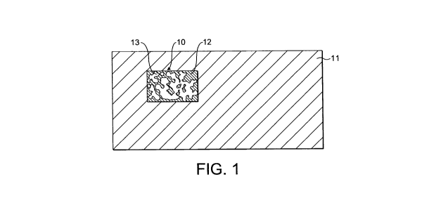
Figure 1 illustrates a security feature 10 of the
present invention formed on a substrate 11, such as a
paper security document. A high resolution image 12 is
applied to the substrate 11 first and a low resolution
image 13 is applied to the high resolution image 12.
Referring to Figure 2, the reflected light
intensity (I) is defined as the light energy flux
incident to or transmitted from a surface. The contrast
ratio (Rb) of the overall image relative to the
background is:-
Rb = ( (Ih+IL) /2) /Ib
CA 02738604 2011-03-25
WO 2010/043846 PCT/GB2009/002327
8 -
The contrast ratio (Rh) of the low resolution
image 13 relative to the high resolution image 12 is:-
Rh = IL/Ih
where:-
Ih is the light intensity of the light reflected from
the high resolution image 12 IL is the light intensity
of the light reflected from the low resolution image 13
Ib is the light intensity of the light reflected from
the background. Ii is the light intensity of the
incident light
It is preferred that Rh << Rb in either the
reflection viewing mode or the transmission viewing
mode or both modes of viewing. It is also preferred
that Rh/Rb < 0.2. The different viewing modes are
shown in Figures 3 and 4, with Figure 3 showing the
reflection mode and Figure 4 showing the transmission
mode.
Preferably the majority of the perimeter of the
low resolution image 13 lies within the perimeter of
the high resolution image 14, and more preferably more
than 80% of the length of the perimeter of the low
resolution image 13 lies within the perimeter of the
high resolution image 12.
The images 12,13 of the security feature 10 can be
formed in a number of different ways. Some of these are
as follows:
CA 02738604 2011-03-25
WO 2010/043846 PCT/GB2009/002327
9 -
a) Print Processes
Print processes represent simple registered
printing in which the low resolution image 13 is
printed over and in register with the high resolution
image 12. The print can be applied to an opaque,
translucent or transparent substrate 11. In the case of
a transparent substrate 11, particular effects can be
obtained when the optical properties of the two images
12,13 are different in either transmission or
reflection mode. Examples of this will be given below
when discussing further specific embodiments of the
invention.
b) Resist and etch process
In this method an ink, comprising one or more
optically variable pigments, is used as a resist in the
so called "resist and etch" method of producing
demetallised images. It has been found that the ink,
which is printed using screen or gravure printing
methods, produces a rather low resolution image 13
because of the large pigment particle size and/or
because the particles are used in a low density. The
ink is printed onto the surface of a metallised film,
which is then demetallised by immersing it in sodium
hydroxide before being washed in water. The resultant
security feature 10 comprises a poorly defined printed
optically variable image 13 under which is a well
defined metal image 12.
CA 02738604 2011-03-25
WO 2010/043846 PCT/GB2009/002327
- 10 -
Optically variable pigments suitable for use in
the present invention include cholesteric liquid
crystal pigments, pearlescent pigments and thin film
interference pigments and holographic flakes. When
these optically variable pigments are used in inks, the
resolution of the image 13 is limited both in terms of
the line widths achievable and the sharpness of the
image outline, i.e. the edge definition of the image
.13. This is due to the fact that the optically variable
pigments, are much larger than conventional pigments so
that it is not possible to produce sharply defined
indicia by directly printing the inks containing such
pigments. Optically variable pigments have to have a
diameter of at least 10 m, and more preferably at least
20 microns, and even more preferably at least 30
microns, in order to achieve a good optically variable
effect.
The combination of the non-optically variable
(high resolution) image 12 superimposed by the
optically variable (low resolution) image 13 allows the
security feature 10 to have a sharp outline, provided
that the optically variable pigments do not extend
beyond the periphery of the non-optically variable
image 12. In this case the sharp outline of the
security feature 10 is provided by the substantially
opaque material of the non-optically variable image 12.
This allows a sharp silhouette of the security feature
10 to be viewed in transmitted light, which would not
be possible if the coating containing the coarse
optically variable pigment used to form the low
CA 02738604 2011-03-25
WO 2010/043846 PCT/GB2009/002327
- 11 -
resolution image 13 is printed directly onto a
transparent substrate 11.
Figures 5 to 7 illustrate how the security
features of the present invention solve the problem of
poor edge definition. The security feature 10 is
preferably formed on a transparent substrate 11, by
applying thereto a patterned opaque layer to form the
high resolution image 12, for example of vapour-
deposited aluminium. An optically variable ink,
comprising a coarse pigment, is then printed in
register over the high resolution image 12 to provide
the low resolution image 13, such that image 13 follows
the same edge outline of the image 12. The pigments
present in the ink do not extend beyond the edge of the
first image 12.
When the security feature 10 is viewed in
reflected light from the direction of arrow A, it is
observed to have the optically variable effect of the
optically variable effect ink. Although the optically
variable effect ink has a poor edge definition, as
shown in Figure 6, this is not readily apparent due to
the presence of the high resolution image 12 which
effectively provides a solid frame around the optically
variable image 13. On viewing from the direction of
arrow B in reflected light the security feature 10 will
appear non-optically variable and, in this example,
will have a metallic appearance. On viewing the
security feature 10 in transmitted light from either
direction A,B (Figure 7) a sharp dark silhouette of the
image 12 will be viewed with a high edge definition.
CA 02738604 2011-03-25
WO 2010/043846 PCT/GB2009/002327
- 12 -
The security feature 10 may be formed in a manner
that enables it to be viewed in a substantially
transparent region of an otherwise opaque security
substrate 16, such as a paper or polymer substrate or a
document-made therefrom. In order to achieve this, the
security feature 10 may be applied to a substrate 11,
which is a substantially transparent polymeric carrier
film, to form a security device 19. The high
resolution image 12 is formed by a layer of a
substantially opaque non-optically variable material,
such as a vacuum deposited metallic layer. The low
resolution image 13 is formed by printing a layer of an
optically variable material, such as resinous coating
comprising one or more optically variable pigments.
The security device 19 may subsequently be
incorporated into the security substrate 16 such that
it is viewable from both sides of the substrate 16.
Methods of incorporating security devices 19 in such a
manner are described in EP-A-1141480 and WO-A-03054297.
In the method described in EP-A-1141480, one side of
the security device is wholly exposed at one surface of
the substrate in which it is partially embedded, and
partially exposed in windows at the other surface of
the substrate.
Security substrates may be formed from any
conventional materials, including paper and polymer.
Techniques are known in the art for forming
substantially transparent regions in each of these
types of substrate. For example, WO-A-8300659
describes a polymer banknote formed from a transparent
CA 02738604 2011-03-25
WO 2010/043846 PCT/GB2009/002327
- 13 -
substrate comprising an opacifying coating on both
sides of the substrate. The opacifying coating is
omitted in localised regions on both sides of the
substrate to form a transparent region. WO-A-0039391
describes a method of making a transparent region in a
paper substrate. Other methods for forming transparent
regions in paper substrates are described in EP-A-
723501, EP-A-724519, WO-A-03054297 and EP-A-1398174.
Another method of incorporating a security device
in a security substrate, such that it is viewable from
both sides of the substrate, is described in EP-A-
11.41480. In this method, as illustrated in Figure 8,
the security device 19 is in the form of a wide
elongate element and is selectively exposed on one side
of the security substrate and fully exposed on the
other side to produce a transparent area 17. This
method enables the insertion of considerably wider
security elements into security substrates than other
methods allow.
Figure 9 shows a cross-sectional view of a
security device 19 bearing a security feature 10
according to the present invention that is suitable for
incorporation in a security substrate 16 in the manner
described in EP-A-1141480. The security feature 10 is
formed on a substrate 11, which is a substantially
transparent polymeric carrier film. The high
resolution image 12 in formed on the substrate as
metallised indicia.
CA 02738604 2011-03-25
WO 2010/043846 PCT/GB2009/002327
- 14 -
It is well known how to produce partially
metallised/demetallised films in which no metal is
present in controlled and clearly defined areas. One
way is to selectively demetallise regions using a
resist and etch technique such as is described in US-B-
4652015. Other techniques are known for achieving
similar effects; for example aluminium can be vacuum
deposited through a mask, or aluminium can be
selectively removed from a composite strip of a plastic
carrier and aluminium using an excimer laser.
The low resolution image 13 is then applied by
printing an optically variable ink or coating to, and
in register with, the metallic high resolution image 12
such that the two images 12,13 have the same shape and
follow the same edge profile. Preferably the low
resolution image 13 does not extend beyond the high
resolution image 12. More preferably the low resolution
image 13 is indented relative to the high resolution
image 12 by at least 10 microns, but preferably no
greater than 100 microns. An adhesive coating 18 may be
applied to both sides 14,15 of the device 19 to improve
its adherence with the security substrate 16 when
embedded therein.
In a modification of the above-mentioned method
the resist used in the resist and etch method comprises
optically variable pigments and is used to form the low
resolution second image 13. The use of an optically
variable resist ensures exact register between the low
resolution image 13 formed therefrom and the high
resolution image 12 formed by the remaining metal.
CA 02738604 2011-03-25
WO 2010/043846 PCT/GB2009/002327
- 15 -
Furthermore it has been observed that, when such a
resist is applied to metal, the optically variable
pigments in the resist tend to recede away from the
edge of the resist coating thus ensuring that the
optically variable pigments do not extend beyond the
edge of the metal forming the high resolution second
image 12 as shown in Figure 10. It is to be noted,
however, that this is a schematic figure and the
pigments would not be arranged in such a uniform
manner.
Referring to Figures lla to llc, a further
alternative method utilises a metallised film
comprising a substantially clear polymeric film of BOPP
or the like, which forms the substrate 11, which has an
opaque layer of metal 14 on a first side thereof
(Figure lla). A resist 20 which contains an optically
variable pigment is printed onto metal layer 14 to form
the low resolution image 13 (Figure lib). An example of
a class of suitable resist materials is vinyl
chlorides/vinyl acetate copolymers such as Union
Carbide Ucar resins, Sun VHL 31534, or Wacker Vinnol E
15/45m. The printed metallised film is then partially
demetallised, according to a known demetallisation
process using a caustic wash, which removes the metal
in the regions 15 not printed with the resist 20. The
remaining regions of metal (i.e. those coated with
resist 20) form the high resolution image 12 and
combination of the images 12,13 create optically
variable indicia which are visible when the security
device 19 is viewed under reflected light from the
direction of arrow A. The indicia are also viewable
CA 02738604 2011-03-25
WO 2010/043846 PCT/GB2009/002327
- 16 -
under reflected light from the direction of arrow B,
but in this case they will appear metallic and not
optically variable.
The images 12,13 and/or indicia created by the
images 12,13 preferably take the form of words,
numerals,' patterns and the like. The optically variable
resist 20 can be printed such that the indicia are
formed from regions of the resist 20 thus creating
positive indicia. Alternatively the optically variable
resist 20 may be printed so as to form indicia
negatively, in which case the resulting indicia will be
provided by the demetallised regions 15. The indicia,
however formed, are clearly visible from both sides in
both reflected light and transmitted light due to the
contrast between the demetallised 15 regions and the
remaining opaque regions which form the high resolution
image 12.
The security device 19 is preferably incorporated
into a security substrate 16, using the method
described in EP-A-1141480, such that the low resolution
image 13 is fully exposed on the front of the substrate
16 and the high resolution image 12 is exposed in a .
transparent window 17 on the back of the substrate 16.
When the front of the substrate 16 is viewed, (as shown
in Figure 12), optically variable indicia are observed
which change colour on angle of view for example
switching from red to green as the substrate 16 is
tilted away from normal incidence. When the back of the
security substrate 16 is viewed in reflected light, as
shown in Figure 13, in the area 17 where it is exposed
CA 02738604 2011-03-25
WO 2010/043846 PCT/GB2009/002327
- 17 -
on both sides, the indicia appear metallic. If the
security substrate 16 is viewed in transmitted light, a
sharp silhouette of the indicia is observed due to the
high edge definition of the metallic high resolution
image 12 and the. fact that the optically variable
pigments in the low resolution image 13 do not extend
beyond the edge of the metal. 'The device 19 could also
be reversed so that the optically variable indicia are
visible in the transparent window 17 when viewed from
the back and the metallic indicia visible when viewed
from the front.
The device shown in Figure 9 could also be
incorporated into a security substrate 16 as a
"windowed thread" as described in EP-A-0059056. EP-A-
0059056 describes a method of manufacture of windowed
thread paper on a cylinder mould paper-making machine.
The technique involves embossing the cylinder mould
cover to form raised regions and bringing an
impermeable elongate security element into contact with
the raised regions of the mould cover, prior to the
contact entry point into a vat of aqueous paper stock.
Where the impermeable security element makes intimate
contact with the raised regions of the embossing, no
fibre deposition can occur and windows are formed in
the surface of the paper. After the paper is fully
formed and couched from the cylinder mould cover, water
is extracted from the wet fibre mat and the paper is
passed through a drying process. In the finished paper
the regions of the security element which are exposed
in the windows are visible in reflected light on one
CA 02738604 2011-03-25
WO 2010/043846 PCT/GB2009/002327
- 18 -
side of the paper. This feature is commonly used for
banknotes.
In a windowed thread configuration, the optically
variable indicia will be visible in-reflected light on
one side of the substrate 16 where the windows expose
the security device 19. When viewed in transmitted
light, a sharp silhouette of the indicia will be
observed due to the presence of the underlying metal
high resolution image 12 being in register with the OVI
low resolution image 13. As the security device 19 is
only exposed on one side of the substrate 16 the non-
optically variable metallic indicia will not be visible
in reflected light.
Optically variable pigments having a colour shift
between two distinct colours, with the colour shift
being dependent on the viewing angle, are well known.
The production of these pigments, their use and their
characteristic features, are described in US-B-4434010,
US-B-5059245, US-B-5084351, US-B-5135812, US-B-5171363,
US-B-5571624, EP-A-0341002, EP-A-0736073, EP-A-668329,
EP-A-0741170 and EP-A-1114102. Optically variable
pigments having a viewing angle dependent shift of
colour are based on a stack of superposed thin-film
layers with different optical characteristics. The hue,
the amount of colour-shifting and the chromaticity of
such thin-film structures depend inter alia on the
material constituting the layers, the sequence and the
number of layers, the layer thickness, as well as on
the production process. Generally, optically variable
pigments comprise an opaque totally reflecting layer, a
CA 02738604 2011-03-25
WO 2010/043846 PCT/GB2009/002327
- 19 -
dielectric layer of a low refractive index material
(i.e. with an index of refraction of 1.65 or less)
deposited on top of the opaque layer and a semi-
transparent partially reflecting layer applied on the
dielectric layer.
Alternative optically variable pigments to the
multilayer thin film structures discussed above are
pearlescent pigments. Pearlescent pigments have a
lamellar substrate of low refractive index such as
mica, PET or synthetic mica coated with a metal oxide
of high refractive index, for example silicon oxide,
titanium oxide or iron oxide. Such a structure results
in the appearance of iridescent colours due to
interference occurring through mutual interference of
the incident light and reflected light at the surface
of the metal oxide coating layers coated on their
surfaces and the lamellar substrate surface and at the
coating interface with the metal oxide. Consequently,
if materials having a high refractive index,
transparency, and smooth and uniform optical properties
are used as the coating layer, pigments of high lustre,
with highly iridescent colours due to interference are
obtained.
Pearlescent inks can be obtained from Merck under
the trade name Iriodin .
A further alternative optically variable pigment
is a liquid crystal pigment. Optically variable liquid
crystal pigments are formed from a liquid crystal
polymer which has been cross-linked such that its
CA 02738604 2011-03-25
WO 2010/043846 PCT/GB2009/002327
- 20 -
molecules are fixed in the cholesteric phase. Once the
film is made, it can be fractured to small platelets.
These platelets retain all the optical properties of
cholesteric liquid crystal film and therefore exhibit
an optically variable angular dependent colour
variation. Optically variable liquid crystal pigments
can be obtained from Sicpa under the tradename Oasis .
Experimental evidence has shown that a pigment
level by weight of at least 10% and more preferably at...
least 20% is required to achieve a full coverage of the
optically variable pigment across the surface of the
indicia.
In an adaptation of the foregoing method a second
clear resist 21 is printed on to the vapour deposited
aluminium layer, as illustrated in Figure 14a to 14d.
The clear resist 21 and the optically variable resist
20 can be printed in register or out of register. When
the resulting security device 19 is viewed under
reflected light from the direction of arrow A, both
metallic and optically variable indicia are observed
but, when viewed under reflected light from the
direction of arrow B, all of the indicia appear
metallic.
Figures 15a to 15d show an example of a design
where the optically variable resist 20 and clear resist
21 are not printed in register. The optically variable
resist 20 is printed as an array of stars (Figure 15a)
and the clear resist 21 is printed as a line pattern
CA 02738604 2011-03-25
WO 2010/043846 PCT/GB2009/002327
- 21 -
(Figure 15b). Figures 15c and 15d shows the finished
security device 19, viewed in reflected light from the
direction of arrow A and arrow B respectively, with the
indicia generated from the optically variable resist 20
and the clear resist 21. When viewing the device 19
from the side of arrow A the stars have an optically
variable effect, for example changing colour from gold
to green on changing the angle of view away from normal
incidence. The lines have a reflective metallic
appearance. On viewing the device 19 from the opposite
side both the stars and the lines have a metallic
appearance.
Figures 16a and 16d show a similar set of images
to Figure 15a to 15d but where the optically variable
resist 20 and the clear resist 20 are printed in
register. In this case the optically variable regions
of the low resolution image 13 regions and the metallic
regions of the high resolution images 13 make up a
single design or indicia rather than independent
designs or indicia.
Figure 17 shows a further embodiment of the
invention in which, in some areas, the clear resist 21
overlaps the optically variable resist 20. The presence
of the clear resist over the optically variable resist
modifies the appearance of the optically variable
indicia in the overlapping region as shown in Figure
18.
Figures 19a to 19d illustrate the steps in another
method of forming the security feature of the present
CA 02738604 2011-03-25
WO 2010/043846 PCT/GB2009/002327
- 22 -
invention in which the clear resist 21 is replaced with
a second optically variable resist 23 which has
different optical effect to that of the first optically
variable resist 20, for example a different angular
dependent colourshift. In this example the first
optically variable resist 20 exhibits ared to green
colourshift on changing the angle of view away from
normal incidence and the second optically variable
resist 23 exhibits a green to blue colourshift.
Referring to Figures 15a to 15d the first optically
variable resist 20 is applied as the array of stars and
the second optically variable resist 23 is applied as
the line pattern. When viewing the security feature 10
from the top side the stars exhibit a red to green
colourshift and the lines exhibit a green to blue
colourshift. On viewing the security feature 10 from
the opposite side, both the stars and the lines have a
metallic appearance.
In yet a further embodiment of the invention the
two different optically variable resists 20,23 can
overlap. This would be similar to the structure and
design shown in Figure 18 except that the clear resist
21 is replaced with a second different optically
variable resist 23. In the overlapping regions 22 a
third colour is observed due to the mixing of the two
colours exhibited by the two optically variable resists
at any given angle of view.
A number of other variations can also be made to
the present invention. An optically variable resist can
be used with optically variable print. This embodiment
CA 02738604 2011-03-25
WO 2010/043846 PCT/GB2009/002327
- 23 -
is similar to Figures lla to lic but with a further
optically variable ink applied after the
demetallisation process. In those regions where the
second optically variable ink is applied over a
demetallised area, it is visible from both sides of the
device.
In each of the forgoing examples the images 12,13
may be applied in register or out of register.
The clear resist 21 in Figures 15a to 15d may also
be replaced with a non-optically variable coloured
resist. Preferably the colour of the non-optically
variable resist matches one of the switching colours of
the optically variable resist 20. For example if the
optically variable resist 20 switches from red to green
on tilting the security feature 10 away from normal
incidence and the non-optically variable resist is
coloured red, then on viewing at normal incidence the
top side of the feature 10 will appear a uniform red
colour. On tilting away from normal incidence the
optically variable resist 20 will switch from red to
green and the non-optically variable resist will remain
red. In this manner a latent image security feature 10
can be created.
In a further embodiment the security device 19 may
be transferred to a security substrate 16 in the form
of a stripe or patch. Figure 20 illustrates an example
of a security device 19 suitable for application as a
stripe or patch. The first and second images 12,13 are
formed on a releasable polymeric carrier substrate 11
CA 02738604 2011-03-25
WO 2010/043846 PCT/GB2009/002327
- 24 -
using the previously mentioned resist and etch method
where the resist comprises an optically variable
pigment and is used to form the low resolution second
image 13. The device 19 can be applied to the security
substrate 16 using an adhesive layer 15. The adhesive
layer 15 is applied to either the security device 19,
or the surface of the security substrate 16 to which
the security device 19 is to be applied. After
transfer, the carrier substrate 11 may be removed,
leaving the security feature 10 as the exposed layer as
illustrated in Figure 21.
In order to visualise the optically variable
effect of the second image 13 in reflection the device
19 must be applied over a substantially transparent
area 17 of the security substrate 16. The example in
Figure 22 shows the security device 19 applied over a
transparent region 17 in a polymeric banknote 25. The
polymeric banknote 25 is formed from a transparent
substrate 26 comprising at least one layer of an
opacifying coating 27 on both sides of the substrate
26. The opacifying coating 27 is omitted in localised
regions on both sides of the substrate 26 to form a
transparent region 17. The security device 19 is then
applied over the transparent region 17 such that when
the security feature 10 in the polymeric banknote 25 is
viewed from the direction of arrow A metallic indicia
are observed but, when viewed under reflected light
from the direction of arrow B optically variable
indicia are observed.
CA 02738604 2011-03-25
WO 2010/043846 PCT/GB2009/002327
25 -
Alternatively the security feature 10 of the
present invention could be incorporated in a polymeric
banknote 25 such that it is only visible from one side
of the substrate 26. In this case the security feature
10is applied to the transparent polymeric substrate 26
and on one side of the substrate .26 the opacifying
coating 27 is omitted. This enables the side of the
security feature 10 from which the optically variable
indicia are visible to be viewed, while on the other
side. of the substrate 26 the opacifying coating 27 is
applied over the security feature 10 such that it
conceals the metallic indicia in reflection. On viewing
in transmitted light, a sharp silhouette of the indicia
will be observed due to the presence of the underlying
metal high resolution image 12.
In a further embodiment the transparent substrate
26 of the polymeric banknote 27 provides the supporting
substrate for the security feature 10.
Polymeric banknotes are just one example of a
secure document based on a polymeric substrate. The
present invention is equally applicable to other types
of polymeric security documents.