Note: Descriptions are shown in the official language in which they were submitted.
CA 02740442 2011-05-13
DIELECTRIC WAVEGUIDE FILTER WITH STRUCTURE
AND METHOD FOR ADJUSTING BANDWIDTH
Field of the Invention
The invention relates generally to dielectric waveguide filters and,
more specifically, to a structure and method for adjusting the bandwidth of a
dielectric waveguide filter.
Background of the Invention
Ceramic dielectric waveguide filters are well known in the art. In the
electronics industry today, ceramic dielectric waveguide filters are typically
designed using an "all pole" configuration in which all resonators are tuned
to the passband frequencies. With this type of design, one way to increase
the attenuation outside of the passband is to increase the number of
resonators. The number of poles in a waveguide filter determines important
electrical characteristics such as passband insertion loss and stopband
attenuation. The length and width of the resonant cavities, also known as
resonant cells or resonators, help to set the center frequency of the
waveguide filter.
U.S. Patent No. 5,926,079 to Heine et al. shows a prior art ceramic
dielectric monoblock waveguide filter in which five resonators are spaced
longitudinally in series along the length of the monoblock and an electrical
signal flows through successive resonators in series to form a passband.
Waveguide filters of the type disclosed in U.S. Patent No. 5,926,079 to
Heine et al. are used for the same type of filtering applications as
traditional
dielectric monoblock filters
1
CA 02740442 2011-05-13
with through-hole resonators of the type disclosed in, for example, U.S.
Patent
No. 4,692,726 to Green et al. One typical application for waveguide filters is
use
in base-station transceivers for cellular telephone networks.
It is also well known in the art that the length and width of a ceramic
waveguide filter such as, for example, the ceramic waveguide filter disclosed
in
U.S. Patent No. 5,926,079 to Heine et al., defines and determines the passband
frequency of the waveguide filter while the height/thickness of the waveguide
filter determines the unloaded "Q" of the waveguide filter resonators and
therefore the insertion loss in the passband of the waveguide filter. In US
Patent
No. 5,926,079 to Heine et al., the positioning of blind input/output holes
centrally
in monoblock bridge regions formed between the resonators and in a
relationship
adjacent slots defined in the monoblock provide the necessary external
coupling
bandwidth of the waveguide filter.
The plating of blind input-output holes during the manufacturing process
however has proven unreliable and can lead to unpredictable filter
performance.
The use of plated input/output through-holes has proven satisfactory in
certain
applications including, for example, the relatively thin resonators of
waveguide
delay lines of the type disclosed in US Patent Application Publication No.
2010/0024973. However, coupling with plated input/output through-holes, when
used with thick waveguide filters, limits the external bandwidth to unduly
narrow
band filters.
The present invention is thus directed to a new and novel structure and
method for providing the necessary external bandwidth in a thick waveguide
filter
which includes plated input/output through-holes without an increase in the
insertion loss of the waveguide filter.
Summary of the Invention
The present invention relates generally to a waveguide filter comprising a
monoblock of dielectric material including a plurality of exterior surfaces
and at
least one step including an exterior surface spaced from one of the exterior
surfaces of the monoblock, and at least one input/output through-hole
extending
2
CA 02740442 2011-05-13
through the monoblock, the at least one input/output through-hole defining
first
and second openings in one of the exterior surfaces of the monoblock and the
exterior surface of the at least one step respectively.
In one embodiment, the exterior surface of the at least one step extends
inwardly from the one of the exterior surfaces of the monoblock and defines a
notch in the monoblock and the second opening of the at least one input/output
through-hole terminates in the notch.
In one embodiment, the waveguide filter further comprises an RF signal
bridge defined in the monoblock and the RF signal bridge is located in the
region
of the monoblock with the notch to define a shunt zero.
In one embodiment, the monoblock includes a first end portion including a
first end surface, the notch is defined in the first end portion, and the RF
signal
bridge is located in the monoblock between the first end surface and the at
least
one input/output through-hole.
In one embodiment, the RF signal bridge is defined by a slit extending into
the monoblock and terminating in the notch.
In another embodiment, the exterior surface of the at least one step
extends outwardly from the one of the exterior surfaces of the monoblock.
In one particular embodiment, the present invention is directed to a
waveguide filter comprising a monoblock of dielectric material including a
conductive exterior surface, at least first and second steps, and at least
first and
second input/output through-holes extending through the first and second steps
and defining respective opposed first and second openings in the exterior
surface
of the monoblock and the first and second steps respectively.
The first and second steps are defined by respective first and second
notches defined in the monoblock and the second openings of the first and
second input/output through-holes terminate in the first and second notches
respectively.
In one embodiment, the first and second notches are defined in respective
first and second opposed end portions of the monoblock and a plurality of RF
3
CA 02740442 2011-05-13
signal bridges extend along the length of the monoblock in a spaced-apart
relationship to define a plurality of resonators.
Also, in one embodiment, the first and second end portions include
respective first and second end surfaces and one of the plurality of RF signal
bridges and the first input/output through-hole is located in the first end
portion of
the monoblock with the first notch defined therein in a relationship wherein
the
one of the plurality of RF signal bridges is located between the first end
surface
and the first input/output through-hole to define a first shunt zero.
In one embodiment, the first notch has a length greater than the second
notch.
The present invention also relates to a method of adjusting the bandwidth
of a waveguide filter comprising at least the following steps: providing a
monoblock of dielectric material including an exterior surface, at least a
first step,
and at least a first input/output through-hole extending through the monoblock
and terminating in respective openings in the first step and the exterior
surface of
the monoblock respectively; and adjusting the height of the step relative to
the
exterior surface of the monoblock to adjust the bandwidth of the waveguide
filter.
In the embodiment where the step is defined by a notch defined in the
monoblock, the step of adjusting the height of the step includes the step of
adjusting the height of the notch.
In the embodiment where the step is defined by a projection on the
monoblock, the step of adjusting the height of the step includes the step of
adjusting the height of the projection.
The method may also further comprise the step of adjusting the diameter
of the first input/output through-hole to adjust the bandwidth of the
waveguide
filter.
Other advantages and features of the present invention will be more
readily apparent from the following detailed description of the preferred
embodiments of the invention, the accompanying drawings, and the appended
claims.
4
CA 02740442 2011-05-13
Brief Description of the Drawings
These and other features of the invention can best be understood by the
following description of the accompanying FIGURES as follows:
FIGURE 1 is an enlarged perspective view of one embodiment of a
ceramic dielectric waveguide filter according to the present invention;
FIGURE 2 is an enlarged vertical cross-sectional view of the ceramic
dielectric waveguide filter shown in FIGURE 1;
FIGURE 2A is an enlarged, broken, vertical cross-sectional view of an
alternate embodiment of a ceramic dielectric waveguide filter incorporating an
outwardly projecting end step;
FIGURE 3 is an enlarged perspective view of another embodiment of a
ceramic dielectric waveguide filter according to the present invention
incorporating a shunt zero at one end thereof;
FIGURE 4 is an enlarged vertical cross-sectional view of the ceramic
dielectric waveguide filter shown in FIGURE 3;
FIGURE 5 is a graph depicting the change in the external bandwidth
(MHz) or coupling of a ceramic waveguide filter of the type shown in FIGURES
1,
2, and 2A in response to a change in the size (height/thickness) and direction
of
the steps formed on the ceramic dielectric waveguide filter shown in FIGURES
1,
2 and 2A;
FIGURE 6 is graph depicting the change in the external bandwidth (MHz)
or coupling of a ceramic dielectric waveguide filter of the type shown in
FIGURES
1 and 2 in response to a change in the diameter of the input/output through-
holes
defined in the ceramic dielectric waveguide filter shown in FIGURES 1 and 2;
FIGURE 7 is a graph representing the performance of the ceramic
dielectric waveguide filter shown in FIGURES 1 and 2;
FIGURE 8 is a graph representing the performance of the ceramic
dielectric waveguide filter shown in FIGURES 3 and 4 with a shunt zero
configured above the passband (i.e., a high side shunt zero); and
5
CA 02740442 2011-05-13
FIGURE 9 is a graph representing the performance of the ceramic
dielectric waveguide filter shown in FIGURES 3 and 4 with a shunt zero
configured below the passband (i.e., a low side shunt zero).
Detailed Description of the Embodiments
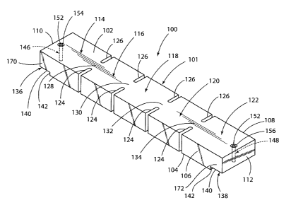
FIGURES 1 and 2 depict one embodiment of a ceramic dielectric
waveguide filter 100 according to the present invention which is made from a
generally parallelepiped-shaped monoblock 101, comprised of any suitable
dielectric material such as for example ceramic, and having opposed
longitudinal
upper and lower horizontal exterior surfaces 102 and 104, opposed longitudinal
side vertical exterior surfaces 106 and 108, and opposed transverse side
vertical
exterior end surfaces 110 and 112.
The monoblock 101 includes a plurality of resonant sections (also referred
to as cavities or cells or resonators) 114, 116, 118, 120, and 122 which are
spaced longitudinally along the length of the monoblock 101 and are separated
from each other by a plurality of spaced-apart vertical slits or slots 124 and
126
which are cut into the surfaces 102, 104, 106, and 108 of the monoblock 101.
The slits 124 extend along the length of the side surface 106 of the
monoblock 101 in a spaced-apart and parallel relationship. Each of the slits
124
cuts through the side surface 106 and opposed upper and lower horizontal
surfaces 102 and 104 and partially through the body of the monoblock 101. The
slits 126 extend along the length of the opposed side surface 108 of the
monoblock 101 in a spaced-apart and parallel relationship and in a
relationship
opposed and co-planar with the respective slits 124 defined in the side
surface
106. Each of the slits 126 cuts through the side surface 108 and opposed upper
and lower horizontal surfaces 102 and 104 and partially through the body of
the
monoblock 101.
By virtue of their opposed, spaced, and co-planar relationship, the slits
124 and 126 together define a plurality of generally centrally located RF
signal
bridges 128, 130, 132, and 134 in the monoblock 101 which extend between and
interconnect the respective resonators 114, 116, 118, 120, and 122. In the
6
CA 02740442 2011-05-13
embodiment shown, the width of each of the RF signal bridges 128, 130, 132,
and 134 is dependent upon the distance between the opposed slits 124 and 126
and, in the embodiment shown, is approximately one-third the width of the
monoblock 101.
Although not shown in any of the FIGURES, it is understood that the
thickness or width of the slits 124 and 126 and the depth or distance which
the
slits 124 and 126 extend from the respective one of the side surfaces 106 or
108
into the body of the monoblock 101 may be varied depending upon the particular
application to allow the width and the length of the RF signal bridges 128,
130,
132, and 134 to be varied accordingly to allow control of the electrical
coupling
and bandwidth of the waveguide filter 100 and hence control the performance
characteristics of the waveguide filter 100.
The waveguide filter 100 and, more specifically the monoblock 101
thereof, additionally comprises and defines respective opposed end steps or
notches 136 and 138, each comprising a generally L-shaped recessed or
grooved or shouldered or notched region or section of the lower surface 104,
opposed side surfaces 106 and 108, and opposed side end surfaces 110 and
112 of the monoblock 101 from which dielectric ceramic material has been
removed or is absent.
Stated another way, in the embodiment of FIGURES 1 and 2, the first and
second steps 136 and 138 are defined in and by opposed end sections or
regions 170 and 172 of the monoblock 101 having a height a (FIGURE 2) less
than the height b (FIGURE 2) of the remainder of the monoblock 101.
Stated yet another way, in the embodiment of FIGURES 1 and 2, each of
the steps 136 and 138 comprises a generally L-shaped recessed or notched
portion of the respective end resonators 114 and 122 defined on the monoblock
101 which includes a first generally horizontal surface or ceiling 140 located
or
directed inwardly of, spaced from, and parallel to the lower surface 104 of
the
monoblock 101 and a second generally vertical surface or wall 142 located or
directed inwardly of, spaced from, and parallel to, the respective side end
surfaces 110 and 112 of the monoblock 101.
7
CA 02740442 2011-05-13
The waveguide filter 100 and, more specifically, the monoblock 101
thereof, additionally comprises first and second electrical RF signal
input/output
electrodes in the form of respective first and second through-holes 146 and
148
extending through the body of the monoblock 101 and, more specifically,
through
the body of the respective end resonators 114 and 122 defined in the monoblock
101 between, and in relationship generally normal to, the surface 140 of the
respective steps 136 and 138 and the upper surface 102 of the monoblock 101.
Still more specifically, each of the generally cylindrically-shaped
input/output
through-holes 146 and 148 is spaced from and generally parallel to the
respective transverse side end surfaces 110 and 112 of the monoblock 101 and
defines respective generally circular openings 150 and 152 located and
terminating in the step surface 140 and the monoblock upper surface 102
respectively.
In the embodiment of FIGURES 1 and 2, the RF signal input/output
through-hole 146 is located and positioned in and extends through the interior
of
the monoblock 101 between and, in a relationship generally spaced from and
parallel to, the side end surface 110 and the step wall or surface 142 while
the
RF signal input/output through-hole 148 is located and positioned in and
extends
through the interior of the monoblock 101 between, and in a relationship
generally spaced from and parallel to, the side end surface 112 and the step
wall
or surface 142.
All of the external surfaces 102, 104, 106, 108, 110, and 112 of the
monoblock 101 and the internal surfaces of the input/output through-holes 146
and 148 are covered with a suitable conductive material such as, for example,
silver with the exception of respective uncoated (exposed ceramic) generally
circular regions or rings 154 and 156 on the monoblock upper surface 102 which
surround the openings 152 of the respective input/output through-holes 146 and
148. Although not shown in any of the FIGURES, it is understood that the
regions 154 and 156 can instead surround the openings 150 defined by the
respective input/output through-holes 146 and 148 in the horizontal surface or
ceiling 140 of each of the steps 136 and 138.
8
CA 02740442 2011-05-13
In accordance with the present invention, the addition in a waveguide filter
of one or both of the respective steps 136 and 138 only in the respective
regions
of the monoblock 101 incorporating the input/output through-holes 146 and 148
(i.e., the regions of the monoblock 101 with the respective end resonators 114
and 122 of reduced height) allows the external bandwidth/coupling/Q value of
the
filter 100 (i.e., a key parameter in the design and performance of bandpass
filters
which is dependent upon the bandwidth of the two end resonators 114 and 122
and has a value which is proportionally higher than the internal bandwidth of
the
filter) to be adjusted with minimal effect on the insertion loss of the filter
100
because the reduction in monoblock height has been restricted only to a small
portion of the monoblock 101.
The addition of one or both of the respective steps 136 and 138 only in the
region of the respective input/output through-holes 146 and 148 also
advantageously allows the monoblock 101 to be manufactured with input/output
through-holes extending fully through the monoblock 101 rather than only
partially therethrough as with the blind holes disclosed in U.S. Patent No.
5,926,079 which are more difficult to manufacture.
Moreover, and although FIGURES 1 and 2 depict a waveguide filter 100
with respective steps 136 and 138 defined by respective recessed or notched
end regions or sections of the monoblock 101 from which dielectric material
has
been removed or is absent (i.e., a "step down" or "step in" region of the
monoblock 101 of reduced height/thickness relative to the height/thickness of
the
remainder of the monoblock 101 which is directed and extends inwardly into the
body of the monoblock from the surface 104 of the monoblock 101), it is
understood that the invention encompasses the alternate waveguide filter
embodiment in which one or both of the notches 136 and 138 have been
replaced or substituted with a projection such as, for example, the projection
138a depicted in the waveguide filter embodiment 100a shown in FIGURE 2A.
More specifically, in FIGURE 2A, the step is defined by an end region or
section 172a of a monoblock 101a having a height a (FIGURE 2A) greater than
the height b (FIGURE 2A) of the remainder of the monoblock 101 (i.e., a "step
9
CA 02740442 2011-05-13
up" or "step out" region or projection 138a of increased thickness/height
relative
to the thickness/height of the remainder of the monoblock 101a which is
directed
and projects outwardly from the lower horizontal longitudinal surface 104a of
the
monoblock 101a.
Thus, more specifically, the monoblock 101 a comprises and defines an
end step or projection 138a comprising an outwardly and exteriorly extending
shouldered region or section of the lower surface 104a, opposed side surfaces
(not shown), and side end surface 112a of the monoblock 101a. Stated another
way, the step 138a comprises an outwardly shouldered portion of the monoblock
101 a and, more specifically, an outwardly shouldered portion of the end
resonator 122a which includes a first generally horizontal exterior surface
140a
located or directed outwardly of, spaced from, and parallel to the lower
surface
104a of the monoblock 101 a and a second generally vertical surface or wall
142a
located or directed inwardly of, spaced from, and parallel to, the respective
side
end surface 112a of the monoblock 101a.
The waveguide filter 100a and, more specifically, the monoblock 101 a
thereof, additionally comprises an electrical RF signal input/output electrode
in
the form of a first through-hole 148a extending through the body of the
monoblock 101 a and, more specifically, extending through the body of the end
resonator 122a between, and in relationship generally normal to, the surface
140a of the step 138a and the upper surface 102a of the monoblock 101a. Still
more specifically, the generally cylindrically-shaped input/output through-
hole
148a is spaced from and generally parallel to the transverse side end surface
11 2a of the monoblock 101 a and defines respective generally circular
openings
150a and 152a located and terminating in the step surface 140a and the
monoblock upper surface 102a respectively.
Thus, in the embodiment of FIGURE 2A, the RF signal input/output
through-hole 148a is located and positioned in and extends through the
interior of
the monoblock 101a between and in a relationship generally spaced from and
parallel to the side end surface 112a and the step wall or surface 142a.
CA 02740442 2011-05-13
In accordance with the embodiment of FIGURE 2A, the incorporation in a
waveguide filter of an outward step or projection 138a only in the region of
the
monoblock 101a incorporating the input/output through-hole 148a allows the
external bandwidth/coupling of the filter 100a to be adjusted with minimal
effect
on the insertion loss of the filter 100a because the increase in monoblock
height/thickness has been restricted only to a small portion of the monoblock
101a.
The addition of the step 138a in the region of the input/output through-hole
148a also advantageously allows the monoblock 101a to be manufactured with
input/output through-holes extending fully through the monoblock 101 a rather
than only partially therethrough as with the blind holes disclosed in U.S.
Patent
No. 5,926,079 which are more difficult to manufacture.
Thus, in accordance with the present invention, the external bandwidth of
a waveguide filter may initially be adjusted either by increasing or
decreasing the
size (i.e., the depth or thickness) of the first and second "step down" or
"step in"
steps 136 and 138 of the waveguide filter 100 depicted in FIGURES 1 and 2 or
by increasing or decreasing the size (i.e., the height) of the "step up" or
"step out"
step 138a shown in FIGURE 2A.
FIGURE 5 is a graph which depicts and represents the simulated change
in external bandwidth (Ext BW (MHz)) of a 2.1 GHz waveguide filter 100 as a
function of D3/b where: Ds (FIGURES 2 and 2A) is either the depth/thickness of
the "step down" or "step in" steps 136 and 138 of the waveguide filter 100
shown
in FIGURES 1 and 2 or the height of the "step up" or "step out" step138a in
the
alternate embodiment described above and shown in FIGURE 2A; and b is the
height/thickness of the monoblock 101. Specifically, it is noted that the
negative
values extending along the x axis represent negative "step down" or "step in"
steps of varying height/thickness while the positive values represent positive
"step up" or "step out" steps of varying height.
The present invention also encompasses and provides another
independent means for adjusting the external bandwidth of the waveguide filter
11
CA 02740442 2011-05-13
100, i.e., by adjusting/varying the diameter of one or both of the first and
second
input/output through-holes 146 and 148.
FIGURE 6 is a graph which depicts and represents the simulated change
in the external bandwidth (Ext BW (MHz)) of a 2.1 GHz waveguide filter 100 as
a
function of d/b where: d is the diameter of the input/output through-holes 146
and
148; and b is the height/thickness of the monoblock 101. Specifically, it is
noted
that the values expressed in percentages (%) along the x axis represent
through-
holes increasing from approximately 6.25% of the total height/thickness b of
the
monoblock 101 to approximately 18.75% of the total height/thickness b of the
monoblock 101.
Although not described herein in any detail, it is further understood that
the performance of the waveguide filter 100 may be adjusted by adjusting the
length of one or both of the steps or notches 136 and 138.
FIGURE 7 is a graph representing the actual performance (i.e., line 162)
of the waveguide filter 100 shown in FIGURES 1 and 2.
FIGURES 3 and 4 depict a second embodiment of a ceramic dielectric
waveguide filter 1100 according to the present invention which incorporates a
step or notch 1138 at one end of the filter 1100 which, in combination with an
RF
signal bridge 1136 and input/output through-hole 1148, define a shunt zero
1180
at one end of the filter 1100 as described in more detail below.
The ceramic waveguide filter 1100, in a manner similar to the waveguide
filter 100, is also made from a generally parallelepiped-shaped monoblock 1101
of dielectric ceramic material having opposed longitudinal upper and lower
horizontal exterior surfaces 1102 and 1104, opposed longitudinal side vertical
exterior surfaces 1106 and 1108, and opposed transverse side vertical exterior
end surfaces 1110 and 1112.
The monoblock 1101 includes a plurality of resonant sections (also
referred to as cavities or cells or resonators) 1114, 1116, 1118, 1120, 1122,
and
1123 which are spaced longitudinally along the length of the monoblock 1101
and are separated from each other by a plurality of spaced-apart vertical
slits or
slots 1124 and 1126 which have been cut into the surfaces 1102, 1104, 1106,
12
CA 02740442 2011-05-13
and 1108 of the monoblock 1101, in the same manner as described above with
respect to the slits or slots 124 and 126 and thus incorporated herein by
reference, to define a plurality of generally centrally located RF signal
bridges
1128, 1130, 1132, 1134, and 1135 on the monoblock 1101, which are similar in
structure and function to the RF signal bridges 128-136 described above and
extend between and interconnect the respective resonators 1114, 1116, 1118,
1120, and 1122.
The waveguide filter 1100 and, more specifically, the monoblock 1101
thereof, additionally comprises and defines respective end steps or notches
1136
and 1138, each comprising a generally L-shaped recessed or grooved or
shouldered or notched region or section of the lower surface 1104, opposed
side
surfaces 1106 and 1108, and opposed side end surfaces 1110 and 1112 of the
monoblock 1101 from which dielectric ceramic material has been removed or is
absent.
Stated another way, and in a manner similar to the steps or notches 1136
and 1138 of the waveguide filter 100 of FIGURES 1 and 2, the first and second
steps or notches 1136 and 1138 of the waveguide filter 1100 comprise opposed
end sections or regions 1170 and 1172 of the monoblock 1101 having a
height/thickness less than the height/thickness of the remainder of the
monoblock 1101.
Stated yet another way, each of the steps or notches 1136 and 1138
comprises a generally L-shaped recessed or notched portion of the monoblock
1101 which includes a first generally horizontal surface 1140 located or
directed
inwardly of, spaced from, and parallel to, the monoblock lower surface 1104
and
a generally vertical surface or wall 1142 located or directed inwardly of,
spaced
from, and parallel to the respective side end surfaces 1110 and 1112 of the
monoblock 1101.
The waveguide filter 1100 and, more specifically, the monoblock 1101
thereof, additionally comprises first and second electrical RF signal
input/output
electrodes in the form of respective first and second through-holes 1146 and
1148 extending between, and in relationship generally normal to, the surface
13
CA 02740442 2011-05-13
1140 of the respective steps or notches 1136 and 1138 and the upper surface
1102 of the monoblock 1101. Still more specifically, each of the generally
cylindrically-shaped input/output through-holes 1146 and 1148 is spaced from
and generally parallel to the respective transverse side end surfaces 1110 and
1112 of the monoblock 1101 and defines respective generally circular openings
1150 and 1152 located and terminating in the step surface 1140 and the
monoblock upper surface 1102 respectively.
In a manner similar to that described earlier with respect to the waveguide
filter 100, it is understood that all of the external surfaces 1102, 1104,
1106,
1108, 1110, and 1112 of the monoblock 1101 and the internal surfaces of the
input/output through-holes 1146 and 1148 are covered with a suitable
conductive
material such as silver with the exception of respective uncoated (exposed
ceramic) generally circular regions or rings 1154 and 1156 on the monoblock
upper surface 1102 which surround the openings 1152 of the respective
input/output through-holes 1146 and 1148. Although not shown in any of the
FIGURES, it is understood that the regions 1154 and 1156 can instead surround
the openings 1150 of respective input/output through-holes 1146 and 1148.
The steps or notches 1136 and 1138 of the waveguide filter 1100 provide
the same advantages and benefits as the steps or notches 136 and 138 of the
waveguide filter 1100, and thus the earlier description of such advantages and
benefits is incorporated herein by reference.
The waveguide filter 1100, however, differs from the waveguide filter 100
in that the waveguide filter 1100 additionally comprises a shunt zero 1180 at
one
end of the monoblock 1101 which is defined and created as a result of the
combination of the incorporation of the following features: an end monoblock
section 1172 of increased or greater length relative to the opposed end
monoblock section 1170 and incorporating and defining an additional end
resonator 1123; a step or notch 1138 extending through the end section 1172
and having a length greater than the length of the step or notch 1136
extending
through the opposed end monoblock section 1170; the placement and location of
the slits 1124 and 1126 defining the RF signal bridge 1135 in the section of
the
14
CA 02740442 2011-05-13
monoblock 1101 including the step or notch 1138 (i.e., in a relationship in
which
the slits 1124 and 1126 defining the RF signal bridge 1135 extend and slice
through the upper longitudinal horizontal surface 1102 of the monoblock 1101
and the lower horizontal surface 1140 of the step or notch 1138 to define the
end
resonator 1123); and the placement and location of the input/output through-
hole
1148 also in the portion of the monoblock 1101 including the step or notch
1138
(i.e, in a relationship wherein the opening 1152 of the input/output through-
hole
1148 is located and terminates in the upper longitudinal horizontal surface
1102
of the monoblock 1101 and the opposed opening 1150 of the input/output
through-hole 1148 is located and terminates in the step or notch 1138 and,
more
specifically, in the horizontal surface 1140 of the step or notch 1138).
Thus, in the embodiment shown, the length of the step or notch 1138 is
such that it extends past both the slits 1124 and 1126 defining the RF signal
bridge 1135 and the RF input/output through-hole 1148 and terminates in a
vertical horizontal wall 1140 located in a portion of the monoblock 1101
defining
the resonator 1122 which is located adjacent the end resonator 1123 and is
separated therefrom by the RF signal bridge 1135.
Still more specifically, in the embodiment of FIGURES 3 and 4, the slits
1124 and 1126 defining the RF signal bridge 1135 and separating the resonators
1122 and 1123 is located in the step or notch 1138 between the input/output
through-hole 1148 and the end surface 1112 of the monoblock 1101. Thus, in
the embodiment shown, the input/output through-hole 1148 is located in the
monoblock 1101 and the notch 1138 between the vertical wall 1142 of the notch
1138 and the slits 1124 and 1126 defining the RF signal bridge 1135.
In accordance with this embodiment of the present invention, the
performance or electrical characteristics of the shunt zero 1180 and thus the
performance of the waveguide filter 1100 may be adjusted and controlled by
varying or adjusting several different parameters including but not limited
one or
more of the following variables or features: the length of the end monoblock
section 1172 and the end resonator 1123; the length L (FIGURE 4) of the step
or
notch 1138; the height/depth/thickness Ds (FIGURE 4) of the step or notch
1138;
CA 02740442 2011-05-13
the position or location of the step or notch 1138 on the monoblock 1101; the
location of the slits or slots 1124 and 1126 along the length of the step or
notch
1138 including the distance between the slits or slots 1124 and 1126 and the
block end surface 1112; the size (i.e., width and depth) of the slits or slots
1124
and 1126 in the step or notch 1138; the location of the input/output through-
hole
1148 along the length of the step or notch 1138; the diameter of the
input/output
through-hole 1148; and the width of the monoblock 1101 and/or the width of the
end resonator 1123 relative to the width of the remainder of the monoblock
1101.
FIGURES 8 and 9 graphically depict and demonstrate the performance
(i.e., attenuation as a function of frequency) of a waveguide filter 1100
incorporating either a high side shunt zero (FIGURE 8) or a low side shunt
zero
(FIGURE 9). Although not shown in any of the FIGURES or described herein in
any detail, it is understood that the length of the shunt zero 1180, and more
specifically the length of the end monoblock section 1172 and the end
resonator
1123, determines whether the shunt zero will be considered a low side shunt
zero or a high side shunt zero and, more specifically, that increasing the
length of
the shunt zero 1180, and more specifically, increasing the length of the end
resonator 1123, will result in a low side shunt zero.
Further, and although not shown or described herein in any detail, it is
understood that a similar high or low side shunt zero can be formed in the
step or
notch 1136 located at the other end of the monoblock 1101 in the same manner
as described above with respect to the shunt zero 1180. Still further, it is
understood that a similar high or low side shunt zero can be formed in the
outward step 138a of the waveguide filter 1100 shown in FIGURE 2A in a
manner similar to that described above with respect to the shunt zero 1180.
While the invention has been taught with specific reference to the
embodiments shown, it is understood that a person of ordinary skill in the art
will
recognize that changes can be made in form and detail without departing from
the spirit and the scope of the invention. The described embodiments are to be
considered in all respects only as illustrative and not restrictive.
16