Note: Descriptions are shown in the official language in which they were submitted.
CA 02740988 2011-04-15
WO 2010/045606 PCT/US2009/061079
TRANSPARENT POLARIZED LIGHT-EMITTING DEVICE
CROSS-REFERENCE TO RELATED APPLICATION
This application claims the benefit of U.S. Provisional Application No.
61/136,965, filed October 17, 2008 and titled TRANSPARENT POLARIZED
LIGHT-EMITTING DEVICE, which is incorporated herein by reference in its
entirety.
TECHNICAL FIELD
This disclosure relates to a transparent polarized light-emitting device.
BACKGROUND
Organic light-emitting diodes (OLEDs) are optoelectronic devices made by
placing a layer of organic material between two electrodes. When a voltage
potential
is applied to the electrodes and current is injected through the organic
material, visible
light is emitted. Due to the high power efficiency, low cost of manufacture,
and
durability of OLEDs, and the fact that they are lightweight, OLEDs are often
used to
create visual displays for portable electronic devices.
SUMMARY
In one general aspect, a transparent directional polarized light-emitting
device
includes a transparent anode and a transparent cathode, a radiation-emitting
layer
between the anode and the cathode, an optically active reflective layer with a
reflection band that matches a chirality and at least partially encompasses a
wavelength band of radiation emitted from the radiation-emitting layer, the
optically
active light blocking layer located on a side of the radiation-emitting layer,
and a
transparent substrate adjacent to the optically active reflective layer.
Implementations may include one or more of the following features. The
radiation-emitting layer may include an organic light-emitting layer. The
radiation-
emitting layer may include an inorganic light-emitting layer. The inorganic
light-
emitting layer may include a quantum dot emitter. The device may include a
hole
transport layer located between the anode and the radiation-emitting layer.
The
device may include an electron transport layer located between the radiation-
emitting
1
CA 02740988 2011-04-15
WO 2010/045606 PCT/US2009/061079
layer and the cathode. The device may include an electron tunneling barrier
layer
located between the cathode and the electron transport layer.
The device may include an electron tunneling barrier adjacent to the radiation-
emitting layer.
The organic light-emitting layer may include a non-racemic compound of
chiral organic light emitting molecules. The organic light-emitting layer may
include
glass-forming chiral nematic liquid crystals (GLCs) that are embedded with
organic
light-emitting dopants, and the organic light emitting layer may emits chiral
light.
The transparent cathode may be a spin polarized electrode. The transparent
cathode may be one of a ferromagnetic electrode and a half-metallic electrode.
The
transparent anode may be a spin polarized electrode. The optically active
reflective
layer may include morphologically stable glass-forming chiral nematic liquid
crystals
(GLCs). The optically active reflective layer may include a cholesteric liquid
crystal.
The device may include a second optically active reflective layer adjacent to
the optically active reflective layer, and a reflection band of the second
optically
active reflective layer may have an opposite chirality to that of the
optically active
reflective layer and may at least partially encompasses a wavelength band of
radiation
emitted from the radiation-emitting layer. The second optically active
reflective layer
may include morphologically stable glass-forming chiral nematic liquid
crystals
(GLCs). The transparent anode and the transparent cathode transmit may visible
light. The optically active reflective layer may include a sculptured thin
film. The
light-emitting layer may include a chiral material.
In another general aspect, a polarized light-emitting device is fabricated by
a
method that includes forming a radiation-emitting layer. The radiation-
emitting layer
includes a radiation-emitting material that emits radiation having a
wavelength
included in an emission wavelength band. The radiation-emitting material is
disposed
between a transparent anode and a transparent cathode. An optically active
reflective
layer is disposed adjacent to the radiation-emitting layer. The optically
active
reflective layer includes glass-forming chiral nematic liquid crystals (GLC),
and the
optically active reflective layer is configured to reflect radiation having a
wavelength
included in a reflection wavelength band of the optically active reflective
layer. The
reflection wavelength band of the optically active reflective layer is
adjusted to at
2
CA 02740988 2011-04-15
WO 2010/045606 PCT/US2009/061079
least partially encompass the emission wavelength band of the radiation-
emitting
layer.
Implementations may include one or more of the following features. The
radiation-emitting material may include an organic light-emitting layer.
Adjusting the
reflection wavelength band of the optically active reflective layer may
include heating
the glass-forming chiral nematic liquid crystals above a glass transition
temperature
(Tg) and near a critical point (Tc) of the glass-forming chiral nematic liquid
crystals.
The optically active reflective layer may be irradiated with electromagnetic
radiation
for a time duration sufficient to alter the reflection wavelength band of the
optically
active reflective layer to at least partially encompass an emission wavelength
band of
the light-emitting layer. The optically active reflective layer may cooled to
a
temperature below (Tg). Irradiating the optically active reflective layer may
include
irradiating the optically active reflective layer with ultraviolet (UV)
radiation.
Adjusting the reflection wavelength band of the optically active reflective
layer may include adjusting a molecular composition of the glass-forming
chiral
nematic liquid crystals. Adjusting the reflection wavelength band of the
optically
active reflective layer may result in changing a width of the reflection
wavelength
band. The radiation-emitting material may include an inorganic light-emitting
layer.
The optically active reflective layer may include a first GLC film made of a
right-
handed glassy cholesteric material, and a second GLC film made of a left-
handed
glassy cholesteric material, the second GLC film being adjacent to the first
GLC film.
Adjusting the reflection wavelength band of the optically active reflective
layer may
include adjusting a molecular ratio of the right-handed glassy cholesteric
material to
the left-handed glassy cholesteric material. The molecular composition of both
the
first GLC film and the second GLC film may be adjusted to adjust the
reflection band
of the optically active reflective layer.
In some implementations, a second optically active reflective layer may be
deposited on the optically active reflective layer. The second optically
active
reflective layer and the optically active reflective layer have opposite
chirality. The
reflection wavelength band of the second optically active reflective layer may
be
adjusted to at least partially encompass the emission wavelength band of the
light-
emitting layer. The optically active reflective layers may be deposited
consecutively,
3
CA 02740988 2011-04-15
WO 2010/045606 PCT/US2009/061079
the reflection wavelength band of the second optically active reflective layer
may be
adjusted on a separate substrate, and the optically active reflective layer
may be
bonded to one side of the transparent polarized light emitting device after
the
reflection wavelength band of the second optically active reflective layer is
adjusted.
In some implementations, the optically active layer is deposited on a
transparent substrate. The transparent substrate may be located between the
optically
active reflective layer and the light-emitting layer.
Implementations of the described techniques may include hardware, a method
or process, a device, an apparatus, or a system. The details of one or more
implementations are set forth in the accompanying drawings and the description
below. Other features will be apparent from the description and drawings, and
from
the claims.
BRIEF DESCRIPTION OF THE DRAWINGS
FIGS. 1 and 2 show examples of a directionally biased light-emitting device.
FIG. 3 shows an example of a directionally biased light-emitting device that
includes two optically active reflective layers.
FIGS. 4A and 4B show examples of a directionally biased light-emitting
device that includes one optically active reflective layer.
FIGS. 5A and 5B show examples of directionally biased light-emitting devices
that include an organic light-emitting diode (OLED) stack.
FIG. 6A shows an example of a directionally biased light-emitting device that
includes an organic light-emitting diode (OLED) stack.
FIG. 6B shows an illustration of emission characteristics from the device
shown in FIG. 6A.
FIG. 7 shows an example process for fabricating a directionally biased light
emitting device.
FIGS. 8A-8C illustrate an example process of pixilating a phototunable liquid
crystal.
FIGS. 9A-11A each show a perspective view of an example directionally
biased light emitting device.
4
CA 02740988 2011-04-15
WO 2010/045606 PCT/US2009/061079
FIGS. 9B-11B respectively show a cross-sectional view of the directionally
biased light emitting devices shown in FIGS. 9A-11A.
FIG. 12 shows a stacked transparent light-emitting device.
FIG. 13 shows another stacked transparent light-emitting device.
DETAILED DESCRIPTION
A transparent device that emits radiation from one side, or primarily from one
side, is described. In particular, an optically active reflective material is
placed on a
transparent electroluminescence device such that radiation emitted from a
light-
emitting layer in the device emanates only from one side of the device, or
primarily
from one side of the device, while ambient light is transmitted by both sides
of the
device. The device emits chiral radiation having a range of wavelengths, and a
reflection band of the optically active reflective material is tuned to match
both the
helicity and the wavelength of the radiation emitted from the device such that
the
optically active reflective material reflects the emitted radiation. In this
manner, the
transparent electroluminescence device may be directionally biased such that
emitted
radiation emanates from only one side of the device, or primarily from one
side of the
device, rather than from both sides of the device.
The disclosed techniques relate to a particular application of organic light-
emitting diode (OLED) technology. In particular, the disclosed techniques
relate to
transparent OLEDs (TOLEDs) that exploit the spin-polarization and the
wavelength
of emitted light to achieve unidirectional emission. The devices are
transparent in that
the devices are made from one or more materials that are at least partially
transmissive to radiation incident upon the materials. Such TOLEDs may be
referred
to as transparent organic unidirectional polarized light-emitting diodes
(TOUPLEDs).
TOUPLEDs may be incorporated into or coated on to windshields to, for example,
allow a driver to see information displayed on the windshield without the
information
being visible from the other side of the windshield. Because the TOUPLED is
transparent to ambient light, ambient light passes through the windshield.
Similarly,
TOUPLED technology may be utilized on helmets, specifically, military combat
helmets or other visualization instruments that include a visor or eyepiece.
With such
an arrangement, the user of the helmet may view information displayed on one
side of
5
CA 02740988 2011-04-15
WO 2010/045606 PCT/US2009/061079
the visor while also being able to see through the visor because ambient light
enters
the visor. For example, the TOUPLED may be mounted on a visor of a military
helmet such that a solider using the helmet may view tactical information
displayed
on the inside part of a helmet visor while the displayed tactical information
would not
be viewable from the side of the visor facing the environment (which is the
side on
which the optically active reflective layer is mounted). However, because the
TOUPLED is made from materials that are at least partially transparent to
ambient
light, ambient light continues to pass through the visor.
Referring to FIG. 1, an example of a directionally biased transparent light-
emitting device 100 is shown. The light-emitting device 100 includes a light-
emitting
layer 1, an optically active reflective layer 2, and a transparent substrate
4. The light-
emitting layer 1 is disposed between a first electrode 5 and a second
electrode 6. The
first electrode 5 may be a transparent anode, and the second electrode 6 may
be a
transparent cathode. The first electrode 5 and the second electrode 6 are
transparent
to the wavelengths of the radiation emitted from the light-emitting layer 1 to
allow
emission of radiation from the device 100. Additionally, the first electrode 5
and the
second electrode 6 may be transparent to ambient light such that ambient light
may
pass through the device 100. Although in the example shown in FIG. 1, the
first
electrode 5 is located at a top 7 of the light-emitting layer 1, and the
second electrode
6 is located at a bottom 8 of the light-emitting layer 1, in other examples,
the first
electrode 5 and the second electrode 6 may be arranged in the opposite
configuration.
When a positive bias is applied across the first electrode 5 and the second
electrode 6, the anode injects holes (positive charge carriers) into the light-
emitting
layer 1, and the cathode injects electrons (negative charge carriers) into the
light-
emitting layer 1. The holes and electrons recombine in the light-emitting
layer 1 and
generate excitons that lead to luminescence. In this manner, the light-
emitting layer 1
emits radiation, preferably in the form of visible light. As discussed in more
detail
below, the radiation emitted from the light-emitting layer 1 has a wavelength
and a
chirality (e.g., the radiation is circularly polarized and has a left-handed
or a right-
handed orientation or the radiation is elliptically polarized and has a left-
handed or a
right-handed orientation).
6
CA 02740988 2011-04-15
WO 2010/045606 PCT/US2009/061079
As discussed in more detail below, the optically active reflective layer 2
blocks the radiation emitted from the light-emitting layer 1 by reflecting the
emitted
radiation back towards the top 7 of the light-emitting layer 1 and into a
light-emission
envelope 9 that is on one side of the device 100. In particular, the optically
active
reflective layer 2 has a reflective band that encompasses, at least partially,
the
wavelengths of the radiation emitted from the light-emitting layer 1. The
reflective
band of the optically active reflective layer 2 is the band of wavelengths
that are not
transmitted by the optically active reflective layer 2. Additionally, the
optically active
reflective layer 2 has a chirality that matches the chirality of the radiation
emitted
from the light-emitting layer 2.
The optically active reflective layer 2 may be considered to match the
chirality
and the wavelength of the radiation emitted from the light-emitting layer 2.
By
matching the chirality and the wavelength, the index of refraction of the
optically
active reflective layer 2 may be tuned, or otherwise modified, such that the
wavelength of the radiation emitted from the light-emitting layer 2 is
centered on the
reflection band of the of the optically active reflective layer 2 and that the
optically
active reflective layer 2 reflects radiation having a helical polarization.
Radiation
having a helical polarization is radiation that has either is elliptically
polarized or
circularly polarized and has either a right-handed or left-handed helicity, or
chirality.
An elliptically or circularly polarized electromagnetic wave in which the
electric field
vector, observed in a fixed plane normal to the direction of propagation while
looking
in the direction of propagation, rotates in a left-handed direction, i.e., in
a
counterclockwise direction, and the direction of propagation is the same as
the
forward direction of a left-handed screw when being screwed into a fixed nut.
In some implementations, matching the chirality and the wavelength may
include tuning the index of refraction of the optically active reflective
layer 2 such
that the optically active reflective layer 2 has a spectral reflection band
that includes at
least a portion of the wavelengths of the radiation emitted from the light-
emitting
layer 2. In these implementations, the optically active reflective layer 2 may
have a
reflection band that is centered on the emission band of the emitted
radiation, but that
is not necessarily the case.
7
CA 02740988 2011-04-15
WO 2010/045606 PCT/US2009/061079
The optically active reflective layer 2 also may be referred to as an
optically
active blocking layer or an optically active filter layer. In the example
shown in FIG.
1, radiation emitted from the light-emitting layer 1 exits the directionally
biased
transparent light-emitting device 100 through the top 7 rather than through
the bottom
8 of the light-emitting layer 1. However, in other examples, the optically
active
reflective layer 2 may be located on the side of the top 7 of the light-
emitting layer 1
such that radiation emitted from the light-emitting layer 1 exits the device
100
through the substrate 4. Thus, the device 100 may be a top-emitting
transparent
device or a bottom-emitting transparent device.
In one implementation, the transparent light-emitting device 100 is a
transparent organic unidirectional polarized light-emitting device (TOUPLED).
In
this implementation, the first electrode 5 is a transparent anode, and the
light-emitting
layer 1 is a chiral organic molecule based light emitting layer (which may be
referred
to as a chiral organic light emitting layer). As discussed below with respect
to FIGS.
5A and 513, the TOUPLED also may include an electron tunneling barrier layer,
a spin
polarized cathode (which may be referred to as a spin-cathode), the
transparent
substrate 4 and, an optically active light filter layer (which may be referred
to as an
optically active reflective layer) tuned to the wavelength and chirality of
the emitted
light. In one example, the chiralty of the optically active reflective layer
may be right
handed such that right-handed circularly polarized light emitted from the
light
emitting device is reflected by the optically active reflective layer 2. In
other
implementations, the light-emitting layer may be made from, or may include,
any
light-emitting material that emits radiation having chiral components (e.g.,
light that is
not linearly polarized).
In another implementation, the light-emitting layer 1 may be an achiral
luminophore. An achiral luminophore is a light emitter that does not
necessarily emit
chiral radiation but may be configured, structured, or arranged to emit chiral
radiation.
For example, in this implementation, the light-emitting layer 1 may be an
inorganic
quantum dot emitter, and the quantum dot emitter may be arranged in a chiral
matrix
that produces chiral radiation. In these implementations, the quantum dot
emitters are
deposited as a single monolayer. Depositing the quantum dot emitters as a
single
8
CA 02740988 2011-04-15
WO 2010/045606 PCT/US2009/061079
monolayer may help localize and, thus, control the formation and relaxation of
excitons.
In other implementations, any transparent OLED layer that is transparent and
does not interfere with the chirality of the emitted and blocked radiation may
be used.
A material that is not optically active, or is weakly optically active, does
not impart a
polarization on radiation passing through the material. Thus, such a material
may be
used as the transparent OLED layer. Materials that may be used as a
transpartent
OLED layer includes glass and ITO. In implementations that use spin-injectors,
any
transparent OLED layer that minimizes interference with the charge-spin life
with the
charge-spin life time or the chirality of the emitted and blocked radiation
may be
used.
Referring to FIG. 2, an example of a directionally biased transparent light-
emitting device 200 is shown. The device 200 includes a light-emitting layer
201, a
optically active reflective layer 202, a transparent substrate 204, a first
electrode 205,
and a second electrode 206. The device 200 may be similar to the device 100
discussed above with respect to FIG. 1, except the transparent substrate 204
is
disposed between the optically active reflective layer 202 and the light-
emitting layer
201. Similar to the device 100, the device 200 emits polarized radiation into
an
emission envelope 209 on one side of the device 200.
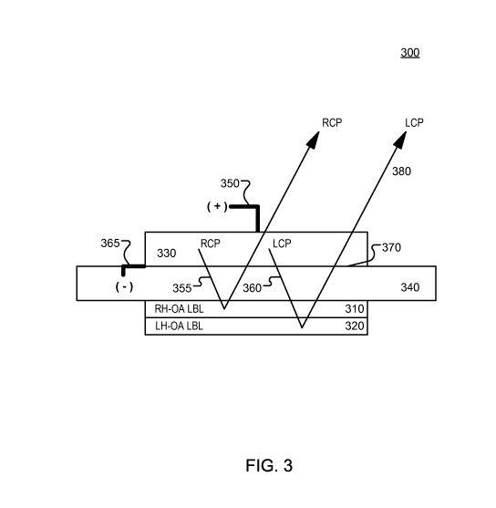
Referring to FIG. 3, an example of a directionally biased light-emitting
device
300 that includes two light-blocking layers, a right-handed optically active
layer 310
and a left-handed optically active layer 320, is shown. The device 300 also
includes a
light-emitting layer 330, a transparent substrate 340, a first electrode 350,
and a
second electrode 365. As discussed in more detail below with respect to FIGS.
5A
and 513, radiation emitted from the light-emitting layer 330 may be chiral
radiation
(e.g., circularly or elliptically polarized light). Depending on the
configuration of the
light-emitting device 300, the chiral radiation may include approximately
equal
amounts of chiral light with right-handed helicity and chiral light with left-
handed
helicity, or the emitted chiral radiation may include primarily chiral light
with right-
handed helicity or primarily chiral light with left-handed helicity.
In the example shown in FIG. 3, the light-emitting layer 330 emits radiation
that includes chiral light with left-handed helicity and chiral light with
right-handed
9
CA 02740988 2011-04-15
WO 2010/045606 PCT/US2009/061079
helicity. Chiral light 355 with right-handed helicity is reflected from the
optically
active reflective layer 310, and the chiral light 360 with left-handed
helicity is
reflected from the optically active reflective layer 320. Thus, the radiation
emitted
from the bottom 370 of the light-emitting layer 330 is reflected through the
top 380 of
the device 300 rather than exiting device through both the bottom 370 and the
top
380. Because the chiralityof helicallypolarized light conserves orientation
upon
reflection off of an optically active material, but reverses orientation upon
reflection
off of a non-optically active material, the chiral light 360 is reflected as
light with
left-handed helicity, and the chiral light 355 is reflected as light with
right-handed
helicity.
Referring to FIGS. 4A and 4B, examples of a directionally biased light-
emitting device 400 that includes one optically active reflective layer 405 is
shown.
The device 400 includes a light-emitting layer 410 formed on a substrate 420.
The
light-emitting layer 410 emits radiation 440 that is circularly polarized and
has a
right-handed helicity. As discussed with respect to FIGS. 5A and 5131 the
helicity of
the radiation emitted from the light-emitting layer 410 may be controlled by,
for
example, introducing a population of spin up electrons into the light-emitting
layer
410. As shown in the example of FIG. 4A, the radiation 440 emitted from the
light-
emitting layer 410, which has right-handed helicity, is reflected from the
optically
active reflective layer 405 and is emitted from a top 450 of the device 400.
The
optically active reflective layer 405 has a reflection band that has a right-
handed
chirality, and, thus, because the radiation 440 is chiral light with right-
handed helicity,
the optically active reflective layer 405 reflects the radiation 440.
Referring to FIG. 4B, the behavior of the device 400 in the presence of
circularly polarized light with left-handed helicity and right-handed helicity
is
illustrated. Circularly polarized radiation 460 with right-handed helicity
emanates
from the device 400 and is reflected from the optically active reflective
layer 405 as
circularly polarized radiation 460 with right-handed helicity. The polarized
radiation
470 is reflected from the optically active reflective layer 405 because the
chirality of
the reflective band of the layer 405 is also right-handed. The radiation 470
is also
reflected off of an object 465, changes orientation upon reflection to
radiation 480,
which has left-handed helicity. Because the radiation 480 has left-handed
helicity, the
CA 02740988 2011-04-15
WO 2010/045606 PCT/US2009/061079
chirality of the reflective band of the optically active layer 405 does not
match the
chirality of the radiation 480. Thus, the radiation 480 passes through the
optically
active reflective layer 405.
As discussed above, a TOUPLED may include one or more of an anode, an
organic light emitting layer, a cathode, a substrate, and an optically active
light
blocking layer. In some implementations, the TOUPLED also includes one or more
of an electron transport layer (ETL), an electron tunneling barrier layer
(TBL), and a
hole transporting layer (HTL). In some implementations, certain
materials/substances
may function as one discrete element described above and herein or may act as
more
than one described above and herein. For example, a particular
material/substance
may be used as an anode and possess certain characteristics of a hole
transport layer.
Referring to FIGS. 5A and 513, examples of directionally biased light-emitting
devices 500A and 500B that include an organic light-emitting diode (OLED)
stack are
shown. Referring to FIG. 5A, the device 500A includes an OLED stack 20, a
substrate 24, a right-handed optically active reflective layer 28, and a left-
handed
optically active reflective layer 29. The OLED stack 20 includes a cathode 21,
electron tunneling barrier layer 27, electron transport layer 25, light-
emitting layer 22,
hole transport layer 26, and anode 23. Anode 23 is adjacent to the substrate
24.
Referring to FIG. 513, the device 500B includes an OLED stack 30, a substrate
34, and
an optically active reflective layer 38. The OLED stack 30 of the TOUPLED may
include a cathode 31, electron tunneling barrier layer 37, electron transport
layer
(ETL) 35, light-emitting layer 32, hole transport layer 36, and anode 33. The
anode
33 is adjacent to the substrate 34.
The directionally biased light-emitting devices 500A and 500B may be
TOUPLEDs. TOUPLEDs may be considered as a series of adjacent layers
consecutively deposited on a substrate. The substrate may be the substrate 4,
the
substrate 204, the substrate 340, the substrate 24 or the substrate 34
discussed above.
Techniques for depositing layers on the substrate include, for example,
chemical
vapor deposition, physical vapor deposition, sputtering, thermal evaporation,
e-beam
deposition, vacuum deposition, spin-coating, and a modification of inkjet
printer
technology. The techniques for depositing layers on the substrate also may be
used to
introduce or "dope" additional compounds into a layer that has been deposited.
For
11
CA 02740988 2011-04-15
WO 2010/045606 PCT/US2009/061079
example, during fabrication of a TOUPLED, an electron transport layer (ETL),
such
as the electron transport layer 25 or the electron transport layer 35
discussed with
respect to FIGS. 5A and 5B, may be deposited and doped with a metal either by
depositing the ETL on an ultra-thin layer of lithium or by depositing the
ultra-thin
layer of lithium on the ETL. Based on the thicknesses of the layers prepared
in this
manner, the lithium may diffuse entirely, from either direction, throughout
the ETL,
thus forming a degenerately-doped ETL. A layer of lithium could also be
deposited
on both sides of the ETL, or the lithium could be co-deposited with the ETL.
The
lithium layer may be deposited such that the layer is about 0.5 to 1.0 nm
thick.
The substrate on which the TOUPLED is fabricated is a material that is
transparent to the chirality and wavelength of the radiation emitted from the
TOUPLED. For example, the substrate may be glass and/or plastic. Polymer films
made from, for example, polyvinylene chloride (PVC), polyethylene
terephthalate
(PET), polyether sulfone (PES), polyethylene naphthalate (PEN), polycarbonate
(PC),
nylon, polyether ether ketone (PEEK), polysulfone (PSF), polyether imide
(PEI),
polyarylate (PAR) and polybutylene terephthalate (PBT) may be used as plastic
substrates.
The TOUPLED may include an anode, which injects positively charged
carriers ("holes") into a light-emitting layer. In some implementations, as
mentioned
above, depending on the particular type of material/substance utilized as an
anode, the
anode also may transport holes into the light-emitting layer. The anode may be
made
from, for example, transparent indium tin oxide (ITO) or In2O3:SnO2. The anode
may
be, for example, the anode 23 or the anode 33 discussed above with respect to
FIGS.
5A and 5B respectively. The light-emitting layer may be the light-emitting
layer 22
or the light-emitting layer 32.
The TOUPLEDs also includes a cathode, such as the cathode 21 or the
cathode 31. Cathodes inject negatively charged carriers or electrons into the
light-
emitting layer. In some implementations, depending on the particular type of
material/substance utilized as a cathode, the cathode also transports
electrons into the
light-emitting layer. Cathode layers may be deposited using, for example, dc
sputtering/cylindrical target deposition. ITO and Indium Zinc Oxide (IZO) are
two
examples of a conductive material for use in manufacturing transparent cathode
12
CA 02740988 2011-04-15
WO 2010/045606 PCT/US2009/061079
layers. Subsequent cathode layers may include a transparent, metallic or non-
metallic
materials and that serve to improve quantum efficiency of the emitting device,
electron injection, minimize work function, and as a protective buffer layer
facilitating the deposition of the ITO on predeposited organic layers; a
transparent
metal-doped cathode layer that may also function as an exciton blocking layer
and/or
as a hole blocking layer; or a transparent, metallic or non-metallic cathode
layer
followed by an electron selective layer made of a material that possesses
different
conductivities for up and down electron spins. Suitable materials for use in
transparent cathodes to facilitate electron transport and injection may
include, but are
not limited to, lithium fluoride (LiF), aluminum (Al), litium-doped aluminum
(Li:Al),
magnesium-doped silver (Mg:Ag), bathocuproine (BCP) (2,9-dimethyl-4,7-diphenyl-
1, 10-phenanthroline), cesium carbonate (CsCO3), lithium-doped bathocuproine
(LiBCP) or cesium-doped phenyldipyrenylphosphine oxide (CsPOPy2).
In order to control the helicity of the chiral light emitted from the TOUPLED,
the population of electrons having a spin up quantum spin state as compared to
the
population of electrons having a spin down quantum spin state may be
controlled.
Electrons exist in two quantum spin states, spin up and spin down, which are
associated with equivalent units of angular momentum values of opposite sign.
A
normally distributed population of electrons is a mixture containing an equal
number
of electrons in the spin up state and in the spin down state. When a normally
distributed population of electrons recombines with holes in a layer of
organic light
emitting molecules, chiral light (e.g., circularly and/or elliptically
polarized light) is
produced. The light emitted is approximately an equal mixture of light with
right
handed helicity (RH) and light with left handed helicity (LH).
In some implementations, however, the TOUPLED may utilize electrons in a
single spin state. When the electrons in a single spin state recombine with
holes in the
TOUPLED, due to quantum spin-selection rules, the emitted chiral light has a
single
handedness (helicity) relative to the emitter molecule orientation. The
helicity of the
emitted light is measured with respect to the emitter molecule's axis of
magnetic
alignment and the sign is a function of the spin state of the injected
electrons and
holes. For example, when electrons in the spin-up state recombine with holes,
chiral
light with right-handed helicity is emitted in a forward direction with
respect to an
13
CA 02740988 2011-04-15
WO 2010/045606 PCT/US2009/061079
aligning magnetic field. When electrons in the spin down state recombine with
holes,
chiral light with left-handed helicity is emitted in a forward direction with
respect to
an aligning magnetic field.
Spin polarized electrons may be produced by, for example, spin filtration via
tunneling and spin polarization via a magnetized injector. Spin filtration via
tunneling
utilizes an electron tunneling barrier layer (TBL) located either adjacent to
the
cathode or sandwiched between two electron transport layers, one of which is
adjacent to the cathode. Electrons in the spin up state have greater momentum
than
electrons in the spin down state. The greater momentum of electrons in the
spin up
state allows these electrons to tunnel through the TBL, while electrons in the
spin
down state are unable to pass through the TBL. Therefore, the TBL enriches the
current flowing in the light-emitting layer with electrons in the spin up
state. The
population of spin up electrons radiatively recombines with holes in the light-
emitting
layer, and, thus, the light-emitting layer emits chiral light with right
handed helicity.
Spin tunneling filtration may yield an electron population with nearly 100%
spin up
electrons. Thus, the emitted radiation is nearly 100% right-handed polarized
radiation. The TBL may be made from, for example, Eu,,Oy (x>>y), which is
selected
for its ability to participate in large exchange splitting in the conduction
band (on the
order of 0.6 eV), and because of its high degree of transparency. Other
materials
having a high degree of transparency and the ability of participate in
exchange
splitting, such as magnesium monoxide and ITO, may be used. Electrons carry
different magnetic momentum depending on the spin state of the electron.
Certain
materials participate in exchange splitting, and in these materials, electrons
in the
spin-up state (which have a higher momentum that electrons in the spin-down
state)
have a higher probability of tunneling through the material. The larger the
exchange
splitting, the more effectively the material discriminates between spin-up and
spin-
down electrons. Thus, in materials having relatively large exchange splitting,
spin-up
electrons have a higher probability of tunneling through the material and, as
a result,
more spin-up electrons pass through. As a result, a spin-polarized current is
generated.
In some implementations, electrons in the spin up state may be produced via a
magnetized injector. A magnetic electron injection cathode, such as chromium
doped
14
CA 02740988 2011-04-15
WO 2010/045606 PCT/US2009/061079
indium tin oxide, forms spin-up polarized electrons that are injected into the
light-
emitting layer. The radiative recombination of electrons in the spin-up state
with
holes results in the emission of chiral light with right-handed helicity. The
electron-
spin selective cathode may be made from, for example, chromium doped indium
tin
oxide (Cr:ITO); chromium doped indium oxide (Cr:IO); any transparent half
metal
(Mo, Zr, Nb, Ru, Tc doped with K2S (about 5% doped)); Zr, Tc, and Ru doped
with
K2O (about 5% doped); or Zr, Nb, and Ru doped with K2Se, K2Te, or Rb2S; any
transparent Hensler alloy; any compound from a class of materials known to be
half-
metallic and having the formula X2YZ, where X and Y are transition elements
(groups
IB to VIIIB on the periodic table) and Z is a group III, IV, or V element.
In some implementations, a magnetized injector may be used in combination
with an electron tunneling barrier layer to achieve a purer spin-polarized
current at a
higher ambient temperature than either the spin filtration or the magnetized
injector
may achieve singly. The magnetized injector may be used to supply a pre-spin
polarized current (e.g., spin-up) to the tunnel barrier that in turn filters
out any
remaining electrons in the spin down state. Polarized electrons in the spin up
state
also may be produced by hybrid spin injecting tunneling filters. Like their
electron
counterparts, holes may be considered as existing in two separate quantum spin
states.
Thus, chiral light of a single helicity may be produced by the radiative
recombination
of electrons with spin polarized holes. Chiral light of a single helicity also
may be
produced by the radiative recombination of spin polarized electrons with spin
polarized holes.
FIG. 6A shows an example of a directionally biased light-emitting device that
includes an organic light-emitting diode (OLED) stack. The example device 600
shown in FIG. 6A is a TOUPLED that includes an organic light-emitting layer
(OLEL) 602 that is transparent. The OLEL 602 includes a cathode 604, an
electron
injection layer 606, an electron transport layer 608, an organic light-
emitting layer
610, a hole transport layer 612, and an anode 614. An optically active
reflective layer
may be disposed on either the cathode or the anode of the stack. In the
example
shown in FIG. 6A, an optically active reflective layer 630 is disposed on the
cathode
604.
CA 02740988 2011-04-15
WO 2010/045606 PCT/US2009/061079
In the example shown in FIG. 6A, the anode 614 includes a conductive anode
of ITO and glass. The ITO layer is approximately forty-two nanometers (42-nm)
thick. The light-emitting layers 602 also include a inter-layer electrical
short
reduction layer 613 made from a layer of molybdenum oxide (Mo03) that is about
20-nm thick, and the hole transport layer 612, which in this example includes
a layer
of N,N' di(naphthalene-1-yl)-N,N'-diphenyl-benzidine (NPB) that is about 55-nm
thick. The light-emitting layer 610 is made of A1g3+C6 and is about 60-nm
thick, and
the electron transport layer 608 is about 40-nm thick and is made of 4,7-
Diphenyl-
1,10-phenanthroline (Bphen). The electron injection layer 606 is about 0.5-nm
thick
and made of lithium fluoride (LiF). In the example of FIG. 6A, the cathode 604
include ITO and aluminum (Al). The ITO layer is about 65-nm thick, and the
aluminum layer is about 100 nm thick. The presence of the aluminum layer
allows
the ITO to be sputtered, or otherwise, applied to the electron injection layer
606.
In another implementation, the cathode may include a conductive cathode of
ITO and glass, an electron injection layer of cesium carbonate (CsC03), an
electron
transport layer of Bphen, a light-emitting layer of A1g3+C6, a hole transport
layer of
Mo03 and NPB, and an anode of silver (Ag) and ITO. The silver portion of the
anode may be a thin layer of silver through which light passes, and the silver
acts as a
protective layer that allows the ITO to be sputtered onto the hole transport
layer.
The device 600 also includes the optically active reflective layers 630. The
optically active reflective layers 630 include a layer of glass 632, and an
alignment
coating 634 that is about 30-40-nm thick and buffed horizontally. A layer of
the
alignment coating 634 is placed on both sides of a right-handed GLC 636, which
is
about 8- m thick, and a layer of glass 638 is disposed on the opposite side of
the GLC
636. An index matching adhesive 640 is disposed on the layer of glass 638, and
an
alignment coating 646 that is buffed vertically and is about 30 to 40-nm thick
is
disposed on both sides of a left-handed GLC 648 that is about 8- m thick. A
layer of
glass 652 and an index matching adhesive layer 654 are also included in the
optically
active reflective layers 630. In the example shown in FIG. 6A, the right-
handed GLC
and the left-handed GLC are both tuned to have a reflection band about 75-nm
wide
and centered at 525-nm.
16
CA 02740988 2011-04-15
WO 2010/045606 PCT/US2009/061079
In either of these implementations, the optically active layers 630 may be
adjacent to the cathode 604 or to the anode 614. In the example of FIG. 6A,
the
optically active layers 630 are adjacent to the cathode 604 and the
directionally biased
light from the device 600 is emitted from the bottom 650 of the device.
The layer thicknesses may be other than specified in the example of FIG. 6A.
In some implementations, the hole transport layer 612 may be a thickness
between 5-
nm and 100-nm, the organic light-emitting layer 610 may have a thickness
between
10-nm to several hundred nm, the electron transport layer 608 may have a
thickness
between 10-nm to several hundred nm, and the thin-metal electron injection
layer 606
(which is aluminum in the example of FIG. 6A), may have a thickness between 10-
nm
and several hundred nm.
FIG. 6B illustrates emission characteristics of the device 600 that is shown
in
FIG. 6A. The emission characteristics include a curve 690 and a curve 695,
each of
which represent intensity as a function of the wavelength of radiation emitted
from
the device 600. The curve 690 shows emissions from the bottom of the device
600,
and the curve 695 shows emissions from the top of the device 600. As seen in
FIG.
6B, the device 600 is directionally biased such that the intensity of
emissions from the
bottom of the device 600 is greater than the emission from the top of the
device 600.
The emissions from the top of the device 600 are mainly attributable to
leakage from
the device 600. However, the emissions from the bottom of the device 600 are
caused
by reflections of the light from the light emitting layers 602 off of the
optically active
layers 630. Thus, the emissions from the bottom of the device 600 are
significantly
greater in intensity than the emissions from the top of the device 600, and
the
emissions from the bottom of the device 600 are centered on a wavelength of
about
525-nm due to the tuning of the reflection bands of the GLC layers 636 and 648
that
are included in the optically active reflective layers 630.
In some implementations, the TOUPLED also may include additional layers
disposed between the anode and the cathode, each layer having different
compositions
and performing different functions. Such materials should be selected for
their charge
mobility characteristics to generate a smooth energy-level transitions
(ionization
potentials) between successive layer interfaces where unrestricted charge
transport is
desired or to generate energy barriers where localization of charge carrier
17
CA 02740988 2011-04-15
WO 2010/045606 PCT/US2009/061079
recombination is desired. Materials may be small molecules or polymers. For
example, the TOUPLED may include an electron transport layer (ETL), such as
the
electron transport layer 35. The ETL may efficiently disperse the injected
current of
negative charge carriers (electrons) across the surface of the layer, and the
ETL
provides a homogenous current at the boundary of the ETL and the layer on the
side
of the ETL opposite from the cathode. The ETL may also serve as a positive
charge
carrier (hole) blocking layer to promote the likelihood and localization of
charge
carrier recombination in the light emitting layer. A spin-polarized electron
transport
layer may improve the probability that the spin polarized state of the
injected
electrons is conserved. Suitable ETL materials include, but are not limited to
4,7-
Diphenyl-1,10-phenanthroline (Bphen), 2,9-Dimethyl-4,7-diphenyl-1,10-
phenanthroline (BCP), or Tris-(8-hydroxyquinolinato)aluminum (A1g3).
In other implementations, a hole transport layer (HTL), such as the hole
transport layer 36, may be provided to efficiently disperse the positive
charge carriers
(holes) across the HTL so that a homogenous current (hole) is provided to the
surface
of the layer adjacent to the HTL, which may be the light-emitting layer. The
HTL
may also serve as a negative charge carrier (electron) blocking layer to
promote the
likelihood and localization of charge carrier recombination in the light
emitting layer.
One or more HTL layers may be used in succession. The HTL may be made from a
host of materials including but not limited to N,N' di(naphthalene-1-yl)-N,N'-
diphenyl-benzidine (NPB), or 4,4'-bis[N(1-napthyl)-N-phenylamino] biphenyl
(alpha-
NPD) (NPD), 1,3,5-Tris(diphenylamino)benzene 97% (TDAB), or from the TDATA
family such as 4,4',4"-tris[2-naphthyl(phenyl)amino]triphenylamine (2-TNATA)
as
small molecule examples, or Poly(2-vinylnaphthalene) as a polymer example.
Dopant
materials may be added to the HTL to improve device lifetime and efficiency.
For
instance, NPB may be doped with molybdenum oxide (Mo03) to reduce the hole
injection barrier, improve interfacial stability, and suppress crystallization
of the HTL.
In some implementations, the materials/substances that function as the ETL or
as the HTL may include the same materials that are incorporated into the light-
emitting layer to produce the electroluminescent emission. If the HTL or ETL
function as the emissive layer (e.g., the light-emitting layer) of such a
device, then the
TOUPLED may be referred to as having a single heterostructure. Alternatively,
a
18
CA 02740988 2011-04-15
WO 2010/045606 PCT/US2009/061079
TOUPLED, having a separate layer of electroluminescent material included
between
the HTL and ETL, may be referred to as having a double heterostructure. Thus,
a
heterostructure for producing electroluminescence may be fabricated as a
single
heterostructure or as a double heterostructure.
In some implementations, one or more buffer layers may be inserted between
successive layers to reduce the abrupt differential barrier height between
successive
layer work-function.
The material properties of the light-emitting layer determine the wavelength
and, hence, the color of the radiation emitted from the OLED. Through
selecting
differing organic solids for the light-emitting layer with a material such as
coumarin 6
(C6), or through doping the organic solid used to make the light-emitting
layer, the
color of the radiation emitted may be varied. In some implementations,
individual
TOUPLED stacks include light-emitting layers that emit light of a particular
color,
and in other implementations, a TOUPLED includes multiple light-emitting
layers
that each emit light of different colors. TOUPLED light emitting materials
with
narrow band emission (saturated color) should be selected Suitable material
for the
light emitting layer include, but are not limited to Tris-(8-
hydroxyquinolinato)aluminum (Alg3), Bis-(8-hydroxyquinolinato)zinc (Znq),
Tris(1,10-phenanthroline)ruthenium(II) chloride hydrate, as small molecule
examples,
or Poly(9,9-di-(2-ethylhexyl)-9H-fluorene-2,7-vinylene) as a polymer example.
Furthermore, in some implementations, the wavelength of the radiation
emitted by the organic light emitting layer (OLEL) may be modified by addition
of
fluorescent and/or phosphorescent materials that absorb the light emitted by
the light-
emitting layer and re-emit radiation of longer wavelength. In some
implementations,
the color of the emitted radiation may be altered by placing a colored or
photoluminescent film between the TOUPLED and the observer.
The TOUPLED also includes an optically active reflective layer, such as the
optically active reflective layer 2, the optically active reflective layer
202, the
optically active reflective layers 405 and 420, the optically active
reflective layer 28
and 29, or the optically active reflective layer 38. The optically active
reflective area
may be an optically-active chiral-light blocking layer (OA-LBL). Materials
suitable
for use as OA-LBLs include, for example, dichroic materials, organic compounds
19
CA 02740988 2011-04-15
WO 2010/045606 PCT/US2009/061079
containing asymmetric carbon atoms, and from inorganic compounds such as glass-
forming chiral nematic liquid crystals (GLC), and chiral dielectric sculptured
thin film
wavelength selective reflectors. Furthermore, the layers that function as OA-
LBL
may be deposited using methods similar to those used to deposit the other
layers of a
TOUPLED. Sculptured thin films are fabricated using a technique that involves
controlling the motion of the substrate on which the film is fabricated during
the
fabrication process. Typically, fabrication of the sculptured thin film
involves
computerized control of the rotation of the substrate about two axis during
the
deposition process.
In one implementation, the OA-LBL may include a GLC layer which is a
cholesteric thin film including a helical stack of quasinematic liquid crystal
layers.
The optical properties of the GLC film are determined to a large degree by the
chirality (i.e. Right- or Left-handedness) and helical pitch length. The
chirality of the
GLC film is determined by the rotational direction of the cumulative nematic
director
twisting which results from the rotation of each successive quasinematic
liquid crystal
layer about the intended optical axis of the film. The helical pitch length
the distance
required to complete a 360-degree rotation of the optical director. A
cholesteric liquid
crystal film may be made of a helical stack of quasi-pneumatic layers, and the
handedness (right-handedness or left-handedness) describes the direction in
which
twisting of the nematic director occurs from one layer to the next. The
helical pitch
length is the distance along the direction of propagation of radiation through
the
layers over which the director rotates 360 .
Cholesteric liquid crystals may be derived from nematic liquid crystals that
have been doped with very low concentrations of chiral dopants, and the
cholesteric
pitch of the cholesteric phases is sensitive to structural modifications of
the chiral
dopant. Thus, the initial helical pitch is largely determined by the selection
of a
particular chiral dopant, and the reflection band of the GLC layer may be set
by
selecting a particular dopant molecule without necessarily performing
subsequent
photomodulation on the GLC layer. The ability of the GLC film to selectively
reflect
a given wavelength is governed a relationship between the helical pitch length
and the
extraordinary and ordinary refractive indices of the quasi-nematic layers. The
differential between these extraordinary and ordinary refractive indices
determines the
CA 02740988 2011-04-15
WO 2010/045606 PCT/US2009/061079
overall optical birefringence of the GLC film, which, in turn, determines the
width of
the selective reflection wavelength band. The wavelengths associated with this
selective reflection band may be altered by modifying the GLC chemical
composition.
Additionally or alternatively, the reflection band may be tuned by, for
example,
photomodulation of the GLC film or by altering or adjusting the molecular
ratio of the
GLC film. In some implementations, the reflection band may be adjusted using
both
photomodulation and adjustment of the molecular ratio by, for example,
adjusting the
molecular ratio of the matierals in the GLC film and then photomodulating the
GLC
film.
In some implementations, the reflection band of the GLC layer may be
considered to act as an optical notch filter that has a reflection band set
(or tuned) by
adjusting a molecular ratio between the materials from which the GLC film is
made.
For example, the GLC optical notch filter may have two adjacent single-handed
GLC
films, with each film having a chirality that is opposite from the chirality
of the other
film. In this implementation, each GLC film includes an appropriate ratio of
right-
handed (R) and left-handed (S) glassy cholesteric material such as, for
example,
2N1CH-R and 2N1CH-S, respectively. A ratio of the left-handed glassy
cholesteric
material to the right-handed glassy cholesteric material may be adjusted to
tune the
reflection band of the GLC film. This ratio may be referred to as the GLC
ratio and
may be considered to be a molecular ratio of the right-handed (R) glassy
choloesteric
material to the left-handed (S) glassy cholesteric material. For example, a
GLC ratio
of S-to-R molecules of 81:19 results in an enantiomeric excess of "S"
molecules that
yields a single left-handed film in a particular wavelength range. The
opposite GLC
ratio (S-to-R of 19:81) results in an enantiomeric excess of "R" molecules
that yields
a single right-handed film at the same, or almost the same, wavelength range.
Adjusting the GLC ratio shifts the reflection band of the GLC film, and may
thus be
considered to tune the GLC film. Additionally, the molecular composition of
the
glassy cholesteric material may be modified to adjust the width of the optical
notch
(e.g., the spectral width of the reflection band). An example structure of a
GLC
molecule from U.S. Patent No. 7,001,648, which is herein incorporated by
reference
21
CA 02740988 2011-04-15
WO 2010/045606 PCT/US2009/061079
in its entirety, as shown below.
R and S
COO(CH2)2 h_\ COO ~CONHH 0
& CH3
NC ~_~ OOC ~_~ O(CH2)3000 COO(CH2)3O COO-// _~ ' CN
In implementations having multiple GLC films, the GLC films may be
adjacent to each other by overlapping, or partially overlapping, each other
such that
radiation that is incident on one of the GLC films and propagates through the
GLC
film is also incident on the other GLC film. The adjacent GLC films may
overlap by
making contact with each other, or the GLC films may be positioned close to
each
other, without necessarily touching each other, such that radiation passes
from one
film to the other. The GLC films may be aligned such that the optical director
of one
GLC film is perpendicular to the optical director of the other GLC film.
In some implementations, the GLC reflection band wavelength may be
increased or decreased by completing a photomodulation process on a deposited
GLC
film. In some implementations, the photomodulation process includes heating
the
GLC thin film to a point above the glass transition temperature of the film
(Tg)
followed by a period of irradiation with ultraviolet (UV) radiation. The glass
transition temperature of the film depends on the chemical composition of the
film.
The GLC thin film also may be heated to a temperature near a critical
temperature
(Tc) of the film. For example, a GLC with Tg of 68 C and Tc of 134 C may be
heated to 120 C (thus the GLC thin film is heated to a temperature of 14 C
from the
Tc). The heating is followed by a period of UV irradiation with, for example,
UV
radiation having a wavelength of 334 nm and an intensity of 70 mW/cm2.
The longer the exposure time to the UV radiation, the longer the resulting
nematic liquid crystal helical pitch length, and hence the longer the
selective
reflection band wavelength of the GLC thin film. The irradiation time is
dependant
on the initial (unmodulated) reflection band, but the irradiation time is a
time duration
that is sufficient to alter the reflection wavelength band of the GLC thin
film. The
closer the initial reflection band is to the final desired reflection band,
the shorter the
required irradiation. Typically, within the visible spectrum, irradiation
times may last
22
CA 02740988 2011-04-15
WO 2010/045606 PCT/US2009/061079
from tens of seconds, to tens of minutes. For example, the irradiation time to
shift the
reflection band from 400nm to 550 nm may be about 10 minutes, whereas the band
shift from 400nm to 750 nm may be about 40 minutes. The radiation used to
irradiate
the GLC film may be unpolarized UV light. UV light is used if only a GLC
optical
notch filters (stacked left- and right- handed GLC filters) are being
simultaneously
photomodulated (e.g., tuned).
The film is then cooled to a point below (Tg; typically room temperature) at
which point the attained selective reflection wavelength becomes frozen in the
solid
state of the GLC thin film.
In some GLC materials the photomodulation process is reversible, where
heating of the GLC thin film with a predetermined selective reflection band
above
(Tg) followed by irradiation of the film with a shorter wavelength than the
selective
reflection band for a sufficient period of time decreases the helical pitch
length of the
nematic liquid crystal, thereby decreasing the wavelength of the GLC selective
reflection band. Subsequent cooling to a point below Tg will freeze the
reflection
wavelength in the solid state of the GLC thin film.In the TOUPLED application,
in
one implementation, a GLC OA-LBL layer of a given chirality (left- or right-
handed)
is selected to match the chirality of the helically-polarized light emitting
layer and is
deposited on the exposed side of the TOUPLED substrate. The GLC layer is
subsequently photomodulated (e.g., tuned) to encompass the wavelength band
emitted
by the organic light-emitting layer. The photomodulation process may be
accomplished by using either an external radiation source or light emitted by
the
TOUPLED light emitting layer itself.
In another implementation, the TOUPLED light emitting layer includes a light
emitting layer that achieves a less than ideal degree of helical polarized
emission. In
this implementation, a GLC OA-LBL layer of right-handed chirality and a GLC OA-
LBL layer of left-handed chirality are deposited successively on the exposed
side of
the TOUPLED substrate. Following deposition, both layers are subjected to an
identical photomodulation process to tune the GLC OA-LBL layers to encompass
the
wavelength band emitted by the organic light-emitting layer. The
photomodulation
process may be accomplished by using either an external radiation source or
light
emitted by the TOUPLED light emitting layer itself. Chiral light with a right
handed
23
CA 02740988 2011-04-15
WO 2010/045606 PCT/US2009/061079
helicity may be reflected by the right-handed OA-LBL and chiral light with
left
handed helicity may be reflected by the left-handed OA-LBL. Electrons in the
spin-
up state produce a chiral light wave with right handed helicity, that in turn
may be
reflected by the right-handed OA-LBL. The result is a transparent device that
emits
chiral light only from that side of the device that does not have the OA-LBL
layer or
layers.
Ambient light is randomly polarized and includes a combination of waveforms
polarized in all orientations. The majority of ambient light is of a
wavelength that is
outside of the OA-LBL stop band (which also may be referred to as the
reflection
band) and is therefore transmitted by the OA-LBL layer. The relatively small
portion
of ambient light that falls into the OA-LBL stop band and that also matches
the
chirality of the OA-LBL is reflected. Chiral light produced within the TOUPLED
from a population of electrons in the spin up state, for example, may be
emitted from
the top of the device and absorbed or reflected by the OA-LBL on the bottom of
the
device. In contrast, the device is equally transparent to ambient light
passing through
the device in either direction.
Referring to FIG. 7, an example process 700 for fabricating a directionally
biased light emitting device is shown. The polarized light emitting device may
be a
TOUPLED as discussed above. A radiation-emitting layer is formed (710). The
radiation-emitting layer includes a radiation-emitting material is disposed
between a
transparent anode and a transparent cathode. The radiation-emitting material
has a
spectral emission band such that all radiation, or almost all radiation,
emitted from the
radiation-emitting material has a wavelength that falls within the emission
band. The
emission band of the radiation-emitting material depends on properties, such
as index
of refraction, of the material from which the radiation-emitting layer is
made. The
radiation-emitting material may be a light-emitting layer made from an organic
material such as, for example, A1g3+C6. The radiation-emitting material may be
a
light-emitting layer such as the light-emitting layers 7, 201, 330, 410, 22,
and 32
discussed above.
An optically active reflective layer is deposited adjacent to the radiation-
emitting layer (720). Thus, the optically active reflective layer may be on
the anode
side or the cathode side of the radiation-emitting layer. The optically active
reflective
24
CA 02740988 2011-04-15
WO 2010/045606 PCT/US2009/061079
layer may include glass-forming chiral nematic liquid crystals, and the
optically active
reflective layer has a spectral reflection band that may be referred to as the
reflection
wavelength band. The optically active reflective layer reflects radiation that
has a
wavelength within the reflection band. The optically active reflection layer
transmits
little, if any, radiation that has a wavelength in the reflection band and
possesses the
same chirality as the optically active reflection layer (because the optically
active
reflection layer reflects such radiation). The optically active reflective
layer may be
deposited on a transparent substrate such as the transparent substrates 4,
204, 340,
420, 24, and 34 discussed above. The transparent substrate may be located
between
the optically active layer and the radiation-emitting layer, but that is not
necessarily
the case. The optically active reflective layer may include a first glassy
liquid crystal
(GLC) film made of a right-handed material and a second GLC film made of a
left-
handed material that is adjacent to the first GLC film.
The reflection wavelength band of the optically active reflective layer is
adjusted to at least partially encompass the emission wavelength band of the
radiation-emitting layer (730). Thus, after the reflection wavelength band of
the
optically active layer is adjusted, the optically active layer reflects
radiation that is
emitted from the radiation-emitting layer. However, because the layers of the
device
are transparent to ambient light, a user of the device is able to see through
the device.
Thus, as discussed below, the device may be used for in-line-of-sight
illumination
applications. As discussed above, adjusting the optically active reflection
layer may
include photomodulating the optically active reflection layer, adjusting the
molecular
composition of the optically active layer, or photomodulating the optically
active
layer after adjusting the molecular composition of the optically active layer.
A second optically active layer may be deposited on the optically active layer
deposited in (720). The second optically active layer has a chirality that is
opposite
that of the optically active layer deposited earlier. Thus, if the earlier-
deposited
optically active layer has a left-handed chirality, the second optically
active layer has
a right-handed chirality. The reflection wavelength band of the second
optically
active layer may be adjusted separately from the first optically active
reflection band
and adjusted on a separate substrate. Once the reflection band of the second
optically
CA 02740988 2011-04-15
WO 2010/045606 PCT/US2009/061079
active layer is adjusted, the second optically active layer may be bonded to
one side of
the TOUPLED device.
The directionally biased transparent light-emitting devices discussed above
such as devices 200, 300, 400, 500A, 500B, and 600 may be used in an
electronic
display, in-line-of-sight illumination applications, and in dual-sided
transparent
display applications. For example, the devices may be used in a non-
transparent flat
panel display and standard applications of flat panel displays, and the
devices may be
used in transparent flat panel electronic displays including active matrix-
based
displays having a thin film transistor (TFT) backplane, passive matrix-based
displays,
monochrome displays, or full-color displays. To use the device in an
electronic
display, the GLC layer may be pixilated such that portions of the GLC layer
are
individually addressable.
To use the light-emitting device in an monochrome display, a single optically
active layer (e.g., a GLC or sculptured thin film) that is shared by all, or
multiple,
pixels that make up the display) may be used. For full-color displays in which
sets of
red, green, and blue pixels are arranged in a spatial pattern and used to make
a multi-
color display, the reflection band of various portions of the GLC layer may be
selectively tuned by exposing the various portions of the GLC layer to
photomodulation. In this manner, the GLC may be considered to be pixilated.
FIGS. 8A-8C illustrate a process for pixilating a GLC, or other phototunable
optically active material.
Referring to FIG. 8A, a red-light emitting layer 810, a green-light emitting
layer 812, and a blue-light emitting layer 814 are deposited on a glass
substrate 820.
Each of the red-light emitting layer 810, the green-light emitting layer 812,
and the
blue-light emitting layer 814 may be OLEDs that emit, respectively, red light,
green
light, and blue light. A phototunable optically active reflective layer 825 is
disposed
on the emitting layers 810, 812, and 814.
Referring to FIG. 8B, a shadow mask 830 having openings 832 and 834 is
positioned above the phototunable optically active reflective layer 825. The
openings
832 and 834 are sized to correspond to a size of a pixel to be formed on the
optically
active reflection layer 825. UV radiation 840 is directed towards the shadow
mask
825 and passes through the openings 832 and 834 to irradiate portions 826 and
827,
26
CA 02740988 2011-04-15
WO 2010/045606 PCT/US2009/061079
respectively, of the optically active reflecting layer 825. The portions 826
and 827 are
exposed to the UV radiation 840 for a sufficient amount of time to tune the
reflection
band of the portions 826 and 827 such that the portions 826 and 827 reflect
red light
having a helicity that is the same as that of the layer 825. Subsequently, the
shadow
mask 830 may be repositioned (not shown) relative to the optically active
layer 825
such that other portions of the optically active reflective layer 825 are
exposed to the
UV radiation 840. As a result, the reflection band of each of these portions
is tuned to
reflect red, green, or blue light depending on the time duration of the
exposure the UV
radiation 840.
Referring to FIG. 8C, the localized irradiation of the optically active
reflecting
layer 825 has been repeated to produce, in addition to portions 826 and 827,
portions
832, which reflect green light, and portions 834, which reflect blue light.
Thus, the
optically active reflecting layer 825 has been pixilated into portions (which
may be
pixels) that reflect red light, portions that reflect green light, and
portions that reflect
blue light. As a result, light emitted from the light-emitting layers 810,
812, and 814
is reflected from, respectively, the portions 832, 827, and 834 of the
optically active
reflective layer 825 and passes through the transparent substrate 820.
Thus, FIGS. 8A-8C illustrate a process for pixilating an optically active
reflective layer, such as a GLC. However, for applications in which
maximization of
transmission of ambient light is not a priority, instead of pixilating an
optically active
reflective layer into individual pixels or portions having individually
tailored
reflection bands, the optically active layer may be deposited in a continuous
strip,
strips, or sheet that spans the entire height and/or width, or a portion of
the height or
width, of the emitting device. Configurations that use a single, non-pixilated
optically
active reflective layer may be simpler and/or less expensive to manufacture
than an
implementation that includes a pixilated GLC.
FIGS. 9A-11A each illustrate a perspective view of an example configuration
of a directionally biased light-emitting device that includes multiple single
optically
active reflective layers. FIGS. 9B-11B, respectively, show a side-view of a
vertical
cross-section of the configurations shown in FIGS. 9A-11A.
Referring to FIG. 9A, a directionally biased light-emitting device 910
includes
pixels 915, a transparent substrate 920, an optically active layer 925 with a
reflection
27
CA 02740988 2011-04-15
WO 2010/045606 PCT/US2009/061079
band tuned to reflect red light, an optically active layer 930 with a
reflection band
tuned to reflect green light, and an optically active layer 935 with a
reflection band
tuned to reflect blue light. The pixels 915 may be OLEDs that preferentially
emit
light from the bottom (the side in contact with the transparent substrate
920), and each
of the optically active reflective layers 925, 930, 935 are shared among all
pixels 915.
The optically active reflection layers 925, 930, and 935 may be arranged in a
different
order, such as shown in FIGS. 10A and 11A.
In operation, the pixels 915 are transparent to light and are, thus, able to
emit
light from both sides (e.g., from the top and bottom of the pixel). However,
the light
emitted by the pixels 915 is preferentially emitted towards the bottom of the
pixel
(e.g., toward the transparent substrate 920). Light that is emitted from the
bottom of
the pixel passes through the transparent substrate 920 and is reflected from
one of the
layers 925, 930, 935 that has a reflection band that includes the wavelength
and
chirality of the light emitted from the pixel. For example, pixel 918 emits
blue light
that passes from the bottom of the pixel 918 through the substrate 925 and
through the
red layer 925. The light is then reflected from the blue layer 930 and exits
through the
top of the pixel 918 as blue light. The blue light from the pixel 918 does not
reach the
green layer 935. The pixel 919 emits green light that from the bottom of the
pixel
919. The emitted light passes through the red optically active layer 925 and
the blue
optically active layer 930 before the light is reflected from the green
optically active
layer 935. The reflected light is transmitted by the blue optically active
layer 930, the
red optically active layer 925, the substrate 920, and the pixel 919 to exit
the display
910A as green light. The pixel 917 emits red light into the transparent
substrate 920,
and the light is reflected from the red optically active layer 925 and exits
the device
910 as red light.
Referring to FIG. 9B, a side view of a vertical cross-section of the device
910
taken along the line "A" is shown. As shown in FIG. 9B, each of the optically
active
layers 925, 930, and 935 are under the pixels 917, 918, 919. Although not
shown, the
optically active layers 925, 930, and 935 are also under the remaining pixels
915.
Referring to FIG. 10A shows a perspective view of a directionally biased
light-emitting device 1010. The display device 1010 is similar to the device
910
except that the pixels 915 are deposited on the optically active layers 925,
930, and
28
CA 02740988 2011-04-15
WO 2010/045606 PCT/US2009/061079
935 rather than on the transparent substrate 920. In the implementation shown
in FIG.
10A, the optically active layers 925, 930, and 935 are deposited on the
transparent
substrate 920. Thus, in this implementation, light emitted from the bottom of
the
pixel 918 is reflected off of the blue optically active layer 930 without
passing
through the transparent substrate 920. This implementation may result in
improved
performance (e.g., increased brightness from the device 1010) because of, for
example, reduction in losses caused by light passing through the substrate 920
as the
light passes from the pixels 915 to the appropriate optically active layer.
FIG. 10B shows a side-view of a vertical cross-section of the device 1010
taken along the line "B".
FIG. 11A shows a perspective view of a directionally biased light-emitting
device 1100. In the device 1100, the pixels 915 are deposited on the substrate
920,
and the optically active reflective layers 925, 930, 935 are bonded to the
pixels 915.
In this implementation, the optically active reflective layers are formed on a
separate
substrate, tuned such that their respective reflection bands reflect red,
green, or blue
light, and then bonded to the pixels 915. In this implementation, light is
preferentially
emitted from the top of the pixels 915, reflects off of the appropriate
optically active
layer, passes through the pixels 915 again, and exits the device 1100 through
the
transparent substrate 920. In such a design, the substrate 520 may provide
protection
for the pixels 915 as well as a platform for deposition. FIG. 11B shows a side
view of
a vertical cross-section of the device 1100 taken along the line "C".
In the examples shown in FIGS. 9A-11A, the pixels 915 are arranged in a
delta configuration in which pixels that emit a particular color are arranged
along
diagonal lines. However, the pixels 915 may be arranged in other
configurations that
are suitable for RGB displays. For example, the pixels 915 may be arranged in
a
striped pattern that includes alternating contiguous segments of red-light
emitters,
green-light emitters, and blue-light emitters. In another example, the pixels
915 may
be arranged in a mosaic pattern, or a Pentile pattern. The Pentile pattern
is
available from Samsung Electronics Co., LTD. of the Republic of Korea.
Referring to FIG. 12, a stacked transparent light-emitting device is shown. A
single pixel, or emitting layer, 1200 is deposited on a transparent substrate
1205. The
pixel 1200 includes a blue-light emitting layer 1210, an optically active
reflective
29
CA 02740988 2011-04-15
WO 2010/045606 PCT/US2009/061079
layer 1215 that reflects blue light, a green-light emitting layer 1220, an
optically
active reflective layer 1225 that reflects green light, and a red-light
emitting layer
1230, an optically active reflective layer 1235 that reflects red light. In
the
implementation shown in FIG. 12, each of the light-emitting layers 1210, 1220,
and
1230 are associated with a transparent anode (not shown) and a transparent
cathode
(not shown) that controls the emission of light from each of the light-
emitting layers.
The implementation shown in FIG. 12 is different from those shown in FIGS.
9A-11A because each of the light-emitting layers in device 1200 has a
corresponding
optically active reflection layer that is adjacent to the emitting layer.
Thus, in device
1200, light emitted from one of the light-emitting layers is reflected from
the adjacent
layer instead of traveling through multiple layers as may be the case in the
implementations shown in FIGS. 9A-11A. As a result, improved performance
(e.g.,
greater intensity of light emitted from the top of the device 1200) may be
realized due
to the minimization of waveguiding.
Referring to FIG. 13, a TOUPLED as a stacked transparent light-emitting
device is shown. FIG. 13 shows a device 1300 that is pixilated by selective
activation
of portions of a stack of light-emitting layers. The device 1330 includes
various light-
emitting layers, each of which have a corresponding transparent cathode, and
each of
which share a common transparent anode. The common anode is divided into
separate segments, and activation of a particular segment of the anode and one
of the
cathodes causes light from the corresponding portion of the light-emitting
layers to be
emitted.
In greater detail, the device 1300 includes a blue-light emitting layer 1310,
a
green-light emitting layer 1320, and a red-light emitting layer 1330. A
transparent
cathode 1340 contacts the blue-light emitting layer 1310, a transparent
cathode 1350
is positioned between the blue-light emitting layer 1310 and the green-light
emitting
layer 1320, and a transparent cathode 1360 is positioned between the green-
light
emitting layer 1320 and the red-light emitting layer 1330. A transparent anode
1370
is segmented into portions 1371-1375 such that light is emitted from a
particular light-
emitting layer, and from a particular portion of the light-emitting layer,
depending on
which portion of the anode 1370 is activated. For example, activating the
anode
CA 02740988 2011-04-15
WO 2010/045606 PCT/US2009/061079
portion 1372 and the cathode 1360 causes red light 1380 to be emitted from the
red-
light emitting layer 1330.
The device 1300 also includes optically active reflective layers 1385, 1390,
and 1395 deposited on a transparent substrate 1380. The optically active
reflective
layers 1385, 1390, and 1395 are tuned to reflect, respectively, blue light,
green light,
and red light. Continuing with the example of the red light 1380, the red
light 1380
reflects off of the optically active reflection layer 1395, propagates up
through the
other optically active layers 1385 and 1390, neither of which reflect red
light, through
the transparent anode 1370, the light emitting layers 1310, 1320, and 1330,
and the
cathodes 1340, 1360, and 1370 to exit the device 1300 through the transparent
cathode 1370.
Thus, FIGS. 8A-8C, 9A-11A, 9B-11B, 12, and 13 all show a transparent
device that includes an optically active reflective layer that causes the
device to
preferentially emit light from one side of the device. The spectral content of
the
emitted light is controllable through the tuning of the reflection band of the
optically
active layer or layers. A user may see through such a device, thus, in
addition to
displays, in implementations where pixilated optically active reflectors are
used or
where optically active layers with a single chirality (i.e. left- or right-
handed) are
used, these devices may be placed in the line-of-sight of a user and used to
illuminate
a region in view of the user.
In addition to being used in the standard displays mentioned above, the
transparent light emitting device may be used in transparent head-up displays
(HUDs)
for the display of information or for use in virtual or augmented reality
applications.
A head-up display may be a transparent display that presents visual data in
the line-of-
sight of a user such that the user may view the data without having to look
away from
their usual viewpoint. The TOUPLED discussed above may be used in a variety of
head-up displays. For example, the TOUPLED may be used in vehicular HUD and
general illumination applications such as applications that display
information on a
vehicle's windshield (e.g., aircraft, automobile, motorcycle), automobile
signal lights,
air traffic control, and visual landing aid lighting.
The TOUPLED also may be used in helmet-mounted HUD applications such
as aircraft pilot visor HUDs, combat solider embedded helmet HUDs, embedded
31
CA 02740988 2011-04-15
WO 2010/045606 PCT/US2009/061079
protective helmet visor HUDs used by, for example, search and rescue workers,
and
visors used by athletes, such as football helmet visors. Additionally, the
TOUPLED
may be used in architectural HUD applications, such as digital signage (e.g.
billboards, "spectacular" or architectural displays on buildings), retail
displays used
for narrowcasting, and window-mounted or embedded displays. The TOUPLED also
may be used in personal electronic device applications, such as near-eye head-
up
displays, in which the TOUPLED display device is integrated on to a head
mounted
apparatus such as a pair of eyeglasses, sunglasses or visor. Such devices may
be
utilized for virtual reality or augmented reality applications. In some
implementations, the TOUPLED may be part of a very near-eye display, in which
the
TOUPLED display device is integrated on a curved surface intended for direct
contact
with the eye such as a contact lens. The TOUPLED device also may be used with
personal desktop and laptop computer displays, portable electronics devices
such as
PDAs, cellular phones, digital music players, digital game players, GPS
devices, and
electronic readers.
The TOUPLED also may be used in photo-sensitive devices in which the
TOUPLED transparent display pixel matrix is interlaced with photo-detectors on
an
integrated circuit, such as a Complimentary-Metal Oxide Semiconductor (CMOS)
circuit. The TOUPLED also may be used in stereoscopic displays for three-
dimensional viewing of electronic images. In a stereoscopic display, two
images are
created from a single TOUPLED display device. Each of the images is generated
with spin-polarized TOUPLED pixels that emit pure, or nearly pure, helically
polarized light. Such a system may require the viewer to wear eye-wear
possessing
polarized filtered lenses to permit each eye to perceive the two separate
images
generated by the display.
TOUPLEDs also may be used in dual-sided transparent display applications.
In such displays, two TOUPLED devices are joined so that the respective
optically
active blocking layers of each device are adjacent to each other. Light is
emitted from
each device in opposing directions to create a display that is active on two
sides that
are opposite to each other. The TOUPLED also may be used for illuminating an
area
and in active electro-optical camouflage systems.
32
CA 02740988 2011-04-15
WO 2010/045606 PCT/US2009/061079
TOUPLED devices may be used for in-line-of-sight illumination for task
lighting. For example, TOUPLEDs may be used in a head-mounted apparatus to
provide head-mounted illumination. Because the TOUPLED is transparent and
emits
light from one side, the head-mounted apparatus may be mounted in the line of
sight
of the user such that the region in the line-of-sight of the user is
illuminated while the
user also views the region through the TOUPLED. TOUPLEDs also may be used in
systems that use and/or provide visual feedback. For example, TOUPLED devices
may be integrated on an industrial or medical boroscope lens, a microscope
lens, and
other inspection devices. TOUPLED devices also may be used with or integrated
with cameras.
It is understood that other modifications are within the scope of the claims.
For example, although red, blue, and green light-emitters are discussed above,
other
colors may be used.
33