Note: Descriptions are shown in the official language in which they were submitted.
CA 02742055 2016-05-03
OPHTHALMIC DEVICE WITH EMBEDDED MICROCONTROLLER
CROSS REFERENCE TO RELATED APPLICATIONS
The present invention claims priority to the U.S. Provisional Application No.
61/110,213 entitled Processor Controlled Ophthalmic Device, tiled October 31,
2008;
U.S. Patent Application No. 12/578,720 entitled Processor Controlled
Ophthalmic
Device, filed October 14, 2009; and U.S. Patent Application 12/580,331
entitled
Ophthalmic Device With Embedded Microcontroller, filed October 16, 2009 as a
Continuation-in-Part Application.
FIELD OF USE
The present invention describes an ophthalmic lens including microcontroller
device embedded within the ophthalmic lens, and more specifically, methods of
fabrication of an ophthalmic lens with a media insert embedding a
microcontroller and
one or more components.
BACKGROUND
Traditionally an ophthalmic lens, such as a contact lens or an intraocular
lens
provided a predetermined optical quality. A contact lens, for example, can
provide one
or more of: vision correcting functionality; cosmetic enhancement; and
therapeutic
effects; but only a set of vision correction functions. Each function is
provided by a
physical characteristic of the lens. Basically a design incorporating a
refractive quality
into a lens provides vision corrective functionality. A pigment incorporated
into the
lens can provide a cosmetic enhancement. An active agent incorporated into a
lens can
provide a therapeutic functionality.
To date optical quality in an ophthalmic lens has been designed into the
physical characteristic of the lens. Generally, an optical design has been
determined
and then imparted into the lens during fabrication of the lens, such as, for
example
1
CA 02742055 2011-04-28
WO 2010/051225
PCT/US2009/061780
through cast molding, or lathing. The optical qualities of the lens have
remained static
once the lens has been formed.
However, wearers may at times find it beneficial to have more than one
function for a biomedical device worn in their eye; for example, it would be
advantageous for an ophthalmic lens to have multiple focal powers available to
them in
order to provide sight accommodation. Other functionalities may also be
useful.
Unlike spectacle wearers, who can change spectacles to change an optical
functionality, contact wearers or those with intraocular lenses have not been
able to
change the functional characteristics of their vision correction without
significant
effort.
SUMMARY
Accordingly, the present invention includes an ophthalmic lens with a
microcontroller which is operative to change a state of one or more components
within
an ophthalmic lens. A change in state of a component may provide additional
functionality by the ophthalmic lens. In addition, methods and apparatus for
forming
an ophthalmic lens, with a microcontroller are presented. Some embodiments can
also
include a cast molded silicone hydrogel contact lens with a rigid or formable
energized
insert which additionally includes a microcontroller, wherein the insert is
included
within the ophthalmic lens in a biocompatible fashion.
Generally, a processor and an energy source can be attached to or made a part
of a media insert and the media insert is placed proximate to at least one of
a first mold
part and a second mold part. A reactive monomer mix is additionally placed
between
the first mold part and the second mold part. The first mold part is
positioned
proximate to the second mold part thereby forming a lens cavity with the
energized
media insert and at least some of the reactive monomer mix in the lens cavity;
the
reactive monomer mix is exposed to actinic radiation to form an ophthalmic
lens.
A lens is formed via control of the actinic radiation to which the reactive
monomer
mixture is exposed. The media insert with the microcontroller is included
within the
lens.
DESCRIPTION OF THE DRAWINGS
2
CA 02742055 2011-04-28
WO 2010/051225
PCT/US2009/061780
FIG. 1 illustrates a mold assembly apparatus according to some embodiments of
the
present invention.
FIG. 2 illustrates aspects of an ophthalmic lens with a media insert including
a
microcontroller.
FIG. 3 illustrates an apparatus for placing media insert including a
microcontroller
within an ophthalmic lens mold part.
Fig. 4 illustrates method steps according to some embodiments of the present
invention.
Fig. 5 illustrates method steps according to some additional aspect of the
present
invention.
Fig. 6 illustrates a processor that may be used to implement some embodiments
of the
present invention.
Fig. 7 illustrates a perspective view of some embodiments of an ophthalmic
lens
including a processor and components.
DETAILED DESCRIPTION OF THE INVENTION
The present invention includes methods and apparatus for manufacturing an
ophthalmic lens with a microcontroller incorporated therein. In addition, the
present
invention includes an ophthalmic lens with a microcontroller incorporated into
the
ophthalmic lens.
In the following sections detailed descriptions of embodiments of the
invention
will be given. The description of both preferred and alternative embodiments
are
exemplary embodiments only, and it is understood to those skilled in the art
that
variations, modifications and alterations may be apparent. It is therefore to
be
understood that said exemplary embodiments do not limit the scope of the
underlying
invention.
GLOSSARY
In this description and claims directed to the presented invention, various
terms
3
CA 02742055 2011-04-28
WO 2010/051225
PCT/US2009/061780
may be used for which the following definitions will apply:
Microcontroller: (also sometimes referred to as a microcontroller unit, MCU or
C) as used herein refers to an integrated circuit consisting of a central
processing unit
(CPU) combined with support function circuitry such as a crystal oscillator,
timers,
watchdog timer, serial and analog I/0 etc., program memory in the form of non-
volatile NOR flash or one-time programmable read only memory (OTP ROM) also
often included, as well as some amount of random access memory (RAM). Some
suitable microcontrollers may operate at clock rate frequencies as low as 4
kHz, as this
is adequate for many typical applications, enabling low power consumption
(milliwatts
or microwatts). They will generally have the ability to retain functionality
while
waiting for an event such as a change state controller or other interrupt.
Energized: as used herein refers to the state of being able to supply
electrical
current to or to have electrical energy stored within.
Energy: as used herein refers to the capacity of a physical system to do work.
Many uses within this invention may relate to the said capacity being able to
perform
electrical actions in doing work.
Energy Source: as used herein refers to a device capable of supplying Energy
or
placing a biomedical device in an Energized state.
Energy Harvesters: as used herein refers to a device capable of extracting
energy from the environment and converting it to electrical energy.
Lens: refers to any ophthalmic device that resides in or on the eye. These
devices can provide optical correction or may be cosmetic. For example, the
term lens
can refer to a contact lens, intraocular lens, overlay lens, ocular insert,
optical insert or
other similar device through which vision is corrected or modified, or through
which
eye physiology is cosmetically enhanced (e.g. iris color) without impeding
vision. In
some embodiments, the preferred lenses of the invention are soft contact
lenses made
from silicone elastomers or hydrogels, which include but are not limited to
silicone
hydrogels, and fluorohydrogels.
Lens forming mixture or "Reactive Mixture" or "RMM"(reactive monomer
mixture): as used herein refers to a monomer or prepolymer material which can
be
cured and crosslinked or crosslinked to form an ophthalmic lens. Various
embodiments can include lens forming mixtures with one or more additives such
as:
4
CA 02742055 2011-04-28
WO 2010/051225
PCT/US2009/061780
UV blockers, tints, photoinitiators or catalysts, and other additives one
might desire in
an ophthalmic lens such as, contact or intraocular lenses.
Lens Forming Surface: refers to a surface that is used to mold a lens. In some
embodiments, any such surface 103-104 can have an optical quality surface
finish,
which indicates that it is sufficiently smooth and formed so that a lens
surface
fashioned by the polymerization of a lens forming material in contact with the
molding
surface is optically acceptable. Further, in some embodiments, the lens
forming
surface 103-104 can have a geometry that is necessary to impart to the lens
surface the
desired optical characteristics, including without limitation, spherical,
aspherical and
cylinder power, wave front aberration correction, corneal topography
correction and
the like as well as any combinations thereof
Lithium Ion Cell: refers to an electrochemical cell where Lithium ions move
through the cell to generate electrical energy. This electrochemical cell,
typically called
a battery, may be reenergized or recharged in its typical forms.
Media Insert: as used herein refers to a formable or rigid substrate capable
of
supporting an Energy Source within an ophthalmic lens. In some embodiments,
the
Media Insert also includes one or more variable optic lenses.
Mold: refers to a rigid or semi-rigid object that may be used to form lenses
from
uncured formulations. Some preferred molds include two mold parts forming a
front
curve mold part and a back curve mold part.
Optical Zone: as used herein refers to an area of an ophthalmic lens through
which a wearer of the ophthalmic lens sees.
Power: as used herein refers to work done or energy transferred per unit of
time.
Rechargeable or Re-energizable: as used herein refers to a capability of being
restored to a state with higher capacity to do work. Many uses within this
invention
may relate to the capability of being restored with the ability to flow
electrical current at
a certain rate for a certain, reestablished time period.
Reenergize or Recharge: To restore to a state with higher capacity to do work.
Many uses within this invention may relate to restoring a device to the
capability to
flow electrical current at a certain rate for a certain, reestablished time
period.
5
CA 02742055 2011-04-28
WO 2010/051225
PCT/US2009/061780
Released from a mold: means that a lens is either completely separated from
the mold, or is only loosely attached so that it can be removed with mild
agitation or
pushed off with a swab.
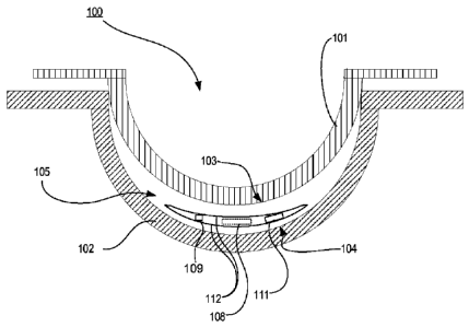
Referring now to Fig. 1, an ophthalmic lens 100 with an embedded
Microcontroller 111 may also include an Energy Source 109, such as an
electrochemical cell or battery as the storage means for the energy and in
some
embodiments, encapsulation and isolation of the materials comprising the
Energy
Source from an environment into which an ophthalmic lens is placed. The Energy
Source 109 can provide power to activate the microcontroller. In some
embodiments,
power consumption of a microcontroller while sleeping (CPU clock and most
peripherals off) may be just nanowatts.
A diagram of an exemplary mold 100 for an ophthalmic lens is illustrated with
a Microcontroller 111. A mold includes a form 100 having a cavity 105 into
which a
lens forming mixture can be dispensed such that upon reaction or cure of the
lens
forming mixture, an ophthalmic lens of a desired shape is produced. The molds
and
mold assemblies 100 of this invention are made up of more than one "mold
parts" or
"mold pieces" 101-102. The mold parts 101-102 can be brought together such
that a
cavity 105 is formed between the mold parts 101-102 in which a lens can be
formed.
This combination of mold parts 101-102 is preferably temporary. Upon formation
of
the lens, the mold parts 101-102 can again be separated for removal of the
lens.
At least one mold part 101-102 has at least a portion of its surface 103-104
in
contact with the lens forming mixture such that upon reaction or cure of the
lens
forming mixture that surface 103-104 provides a desired shape and form to the
portion
of the lens with which it is in contact. The same is true of at least one
other mold part
101-102.
Thus, for example, in a preferred embodiment a mold assembly 100 is formed
from two parts 101-102, a female concave piece (front piece) 102 and a male
convex
piece (back piece) 101 with a cavity formed between them. The portion of the
concave
surface 104 which makes contact with lens forming mixture has the curvature of
the
front curve of an ophthalmic lens to be produced in the mold assembly 100 and
is
sufficiently smooth and formed such that the surface of an ophthalmic lens
formed by
6
CA 02742055 2011-04-28
WO 2010/051225
PCT/US2009/061780
polymerization of the lens forming mixture which is in contact with the
concave
surface 104 is optically acceptable.
A lens forming surface can include a surface 103-104 with an optical quality
surface finish, which indicates that it is sufficiently smooth and formed so
that a lens
surface fashioned by the polymerization of a lens forming material in contact
with the
molding surface is optically acceptable. Further, in some embodiments, the
lens
forming surface 103-104 can have a geometry that is necessary to impart to the
lens
surface any desired optical characteristics, including without limitation,
spherical,
aspherical and cylinder power, wave front aberration correction, corneal
topography
correction and the like as well as any combinations thereof According to the
present
invention, optical characteristics can work in concert with a Microcontroller
111 to
provide an overall optical quality.
According to the present invention, microcontrollers 111 are incorporated into
an ophthalmic lens and used to automatically control components or devices
also
incorporated into the ophthalmic lenses. In the present invention, a
Microcontroller
111 package size is reduced to 2 mm x 2 mm x 0.3 mm thick, preferably less
than
1.5 mm x 1.5 mm x 0.2 mm thick, and more preferably less than about 1.3 mm x
1.3 mm x 0.2 mm thick. Smaller sizes may also be utilized. In some
embodiments, a
mixed signal microcontroller may be included to integrate analog and digital
components. The Microcontroller 111 is included in an embedded system within
the
lens.
Quiescent current of a Microcontroller 111 is desirably lower than 1 microamp
in standby/sleep mode. More preferable would be less than about 500 nA
(nanoamps),
and most preferable would be less than about 250 nA. Low voltage operation
less than
about 3.6 V is preferred. More preferable is operation at lower voltages, such
as, for
example, at 0.9 V DC.
In some preferred embodiments, microcontrollers 111 monitor or track events
in or around the eye and respond to the occurrence of events as the events
occur. An
interrupt system can signal the processor to suspend processing a first
instruction
sequence and to begin an interrupt service routine (ISR, or "interrupt
handler"). The
ISR will perform preprogrammed routines based upon programmable code included
in
7
CA 02742055 2011-04-28
WO 2010/051225
PCT/US2009/061780
the ISR. In some embodiments, the processor will return to the first
instruction
sequence following execution of the ISR.
Interrupt sources may include, by way of non-limiting example, an internal
timer reaching a predetermined value, a logic level change on an input such as
from a
magnetic switch or an optical switch, and data received via a communication
link. In
addition, an ISR may include power management logic that transitions a
microcontroller from a low power sleep state where the processor is halted, to
an active
state wherein the processor is enabled to fully operate.
In another aspect, some embodiments can include programming of the
Microcontroller 111 prior to formation of the ophthalmic lens. Executable
programs
are stored in a memory or other storage device included within the
microprocessor or
in digital communication with the microprocessor. Generally, in preferred
embodiments, if a memory device is external to the microcontroller, it will be
proximate to the microcontroller and connected via a bus.
High-level language and assembler language codes can be compiled into a
compact machine code for storage in the microcontroller's memory. Preferably,
compiled code is stored in memory prior to placement of a Microcontroller 111
within
a mold part used to form an ophthalmic lens, however, in some embodiments,
executable code may be wirelessly transmitted into the microcontroller while
the
Microcontroller 111 is embedded within the contact lens. Accordingly, various
embodiments may include a microcontroller with a stored memory that is
permanent,
read-only memory that can only be programmed prior to placement into an
ophthalmic
lens, or program memory that includes field-alterable flash or erasable read-
only
memory.
Some embodiments include a Microcontroller 111 with an analog to digital
converter. The analog to digital converter is used to convert input to the
microcontroller into digital form that the processor can process. In another
aspect, a
digital to analog converter may be employed to enable the processor to send
data to a
device it is controlling in analog form.
Microcontrollers 111 may also include one or more timers. Timers may
include, for example a Programmable Interval Timer (PIT). A PIT counts down
from
some value to zero. Once it reaches zero, it sends an interrupt to the
processor
8
CA 02742055 2011-04-28
WO 2010/051225
PCT/US2009/061780
indicating that it has finished counting. In some embodiments, a timer in a
microcontroller may be used to return an electro-active lens, such as a lens
with a
liquid meniscus lens portion, to a native state following a command to
transition to an
active state. For example, upon activation, a command from the microcontroller
will
place the liquid meniscus lens in an active state. The liquid meniscus lens
will remain
in the active state for a predetermined period of time and then the
microcontroller will
revert the liquid meniscus lens portion back to the native state. The timer in
the
microcontroller tracks the predetermined period of time. A time processing
unit (TPU)
may also be used in some embodiments. The TPU enables the microcontroller to
count down and also detect input events, generate output events, and perform
other
operations.
Additional components may include, for example, one or more of: a dedicated
Pulse Width Modulation (PWM) block which enable the CPU to efficiently control
micro devices without using lots of CPU resources in tight timer loops;
universal
asynchronous receiver/transmitter (UART) for receiving and transmitting data
over a
serial line with very little load on the CPU.
Essentially a microcontroller is advantageous in some energized ophthalmic
lenses because it can be packaged as a single integrated circuit, with one or
more of: a
central processing unit including 4-bit, 8-bit, 16-bit, 32-bit, and 64-bit
processors;
discrete input and output bits, allowing control or detection of the logic
state of an
individual package pin; serial input/output such as serial ports (UARTs);
other serial
communications interfaces like I2C; timers such as event counters, PWM
generators;
volatile memory (RAM) for data storage; ROM, EPROM, EEPROM or Flash memory
for program and operating parameter storage; one or more clock generators,
such as,
for example an oscillator for a quartz timing crystal and a resonator; analog-
to-digital
conversion (ADC), digital to analog conversion (DAC), temperature sensor,
comparator, capacitive touch sensing, communications protocols such as UART,
I2C,
SPI, or universal serial bus. The microcontroller should have one or more
internal
oscillators, which may include a real time clock, or a "precision" oscillator.
The
microcontroller will preferably include at least 6 general purpose I/O's, more
preferably would be 10, most preferable would be 14 or more.
9
CA 02742055 2011-04-28
WO 2010/051225
PCT/US2009/061780
The use of field-programmable devices on a microcontroller may allow
programming of firmware specific to the need of a particular patient
subsequent to
formation of the lens and prior to a patient wearing the lens. Programmability
can be
accomplished in various ways. In some embodiments system programming is
accomplished via an external connection to the microcontroller from a flex
board.
Additional embodiments include one-time programmable (OTP) devices. Still
other
embodiments include devices programmed at the wafer level, such as during
production of the microcontroller.
In some embodiments, the physical die size will be less than about 2 mm x
2 mm x 0.3 mm thick and preferably less than 1.5 mm x 1.5 mm x 0.2 mm thick,
and
more preferably less than about 1.3 mm x 1.3 mm x 0.2 mm thick. Smaller die
may
also be utilized. In some cases, the lateral dimension may exceed 2 mm, for
example
2.4 mm for a solar cell. One particular embodiment includes a microcontroller
with a
first dimension of 2.4 mm and a second dimension of 1.6 mm.
In some embodiments, the packaging of the microcontroller to be placed within
an ophthalmic lens includes bare die and gold stud bumps, and/or solder bumped
flip
chip, or wafer level chip scale package (WLCSP). The preferred size of the
solder
bumps on the solder bumped flip chip are less than about 100 microns (nominal
ball
diameter), and also preferred would be about 65 micron (nominal ball
diameter). The
pitch of interconnects should desirably be such that high speed pick and place
equipment could place the component in a high speed operation. Current state
of the
art for fine pitch is about 0.3mm pitch. Finer pitches can be placed, but the
equipment
specs are more stringent, and throughput is reduced.
Some embodiments include on board program memory. Due to the nature of
an ophthalmic lens, size constraints generally limit an amount of memory that
may be
included with, or as part of, a Microcontroller 111. Generally, at presently
available
size constraints, the amount of memory may be limited to about 2 kB within the
microcontroller111 in order to minimize die area; however, the history of
substrate
manufacture indicates that increased density of memory chips will enable
additional
memory to be included.
A Microcontroller 111 can provide manipulation of data from within the
confines of an ophthalmic lens. In some embodiments, the manipulation of data
can
CA 02742055 2011-04-28
WO 2010/051225
PCT/US2009/061780
include generating one or more instructions based upon data received. In some
embodiments, the received data can be indicative of a condition proximate to
the lens;
such as, for example: an amount of moisture to which the lens is exposed, a
temperature of a lens surface, a state of an electrowetted device included
within the
lens, or other condition.
Additional embodiments may include a state of a component included within a
lens such as the status of a counter used to time a supply of power to a
component or
an input received by a component. An input received can include, for example,
a
magnetic pulse, a light pattern, a radio frequency signal or other form of
data
communication.
Some additional embodiments can also include the microcontroller issuing a
command to change the state of a liquid meniscus lens portion 108 within an
ophthalmic lens; wherein the change of state of the liquid meniscus lens
portion
changes the optical qualities of the lens.
An instruction generated can include a command to control a component
included within the ophthalmic lens or a command to transmit data from the
ophthalmic lens. By way of non-limiting example, a command to control a
component
included within the ophthalmic lens can include: a predetermined polling cycle
of
receipt of an external signal to activate one ore more components contained
within the
ophthalmic lens. In order to improve efficiency of some components, such as a
magnetic sensing switch or a photoreceptor functioning as an activation
switch, a
processor can be programmed to cause the component to turn on at specific
intervals.
In this manner, for example the magnetic sensing switch may only consume
energy for
10 seconds (or some other interval) each minute of time. Other embodiments,
may
cause the Microcontroller 111 to receive input from a component sensing
temperature
of a lens; surface tension of a lens; pressure on a lens; or other parameter
which is
measurable by an electronic, electromechanical or MEMs device (micro
electromechanical machine device).
A Microcontroller 111 can include, by way of non-limiting example, an ultra-
low power microcontroller 16-bit or 32-bit RISC mixed signal processor.
Preferably
the microcontroller will be sealed, such as hermetically sealed in a ceramic
or other
impervious material. The power consumption is preferably low, such as 250
micro
11
CA 02742055 2011-04-28
WO 2010/051225
PCT/US2009/061780
amps/MIPS active. One example includes the Texas Instruments MSP 430
microprocessor.
In some additional embodiments, the Microcontroller can issue commands to
control a variable focal length lens. The controls can cause an electrical
current to be
applied across two or more transparent borders that generally parallel delimit
an
internal volume containing two non-miscible liquids. The two non-miscible
liquids
will have different optical indices. An elastic element is positioned such
that it will
deform in response to a change in pressure of the liquids. The pressure of the
liquids
changes in response to changes that the instructions from the Microcontroller
causes in
the electrical charge placed across one or both of the liquids.
In some embodiments a Microcontroller 111 controlled variable lens can
include a liquid meniscus lens including a liquid containing cell for
retaining a volume
of two ore more liquids. A lower surface, which is non-planar, includes a
conical or
cylindrical depression or recess, of axis delta, which contains a drop of an
insulating
liquid. A remainder of the cell includes an electrically conductive liquid,
non-miscible
with the insulating liquid, having a different refractive index and, in some
embodiments, a similar or same density. An annular electrode, which is open
facing a
recess, is positioned on the rear face of a lower plate. Another electrode is
placed in
contact with the conductive liquid. Application of a voltage across the
electrodes is
utilized to create electrowetting and modify the curvature of the interface
between the
two liquids, according to the voltage (V) applied between the electrodes. A
beam of
light passing through the cell normal to the upper plate and the lower plate
and in the
region of the drop will be focused to a greater or lesser extent according to
the voltage
applied to the electrodes. The conductive liquid is typically an aqueous
liquid, and the
insulating liquid is typically an oily liquid. Generally, the microcontroller
controls the
application of voltage across the electrodes of a liquid meniscus lens portion
and
thereby controls the optical characteristics of the ophthalmic lens. The
microcontroller
may also monitor and track variables related to the liquid meniscus lens
portion, such
as for example, a current state of optical characteristics.
A user controlled adjustment device can be used to interface with the
Microcontroller and thereby control the focus of the lens. The adjustment
device can
12
CA 02742055 2011-04-28
WO 2010/051225
PCT/US2009/061780
include, by way of non-limiting example, a magnetically activated switch, a
photo-
optically activated switch, an electrical sensor sensing a signal within the
eye to focus,
a radio frequency transmission device or any other electronic device or
passive device
for providing a user supplied instruction to the processor.
In some embodiments, a lens with a Microcontroller 111 placed on a media
which includes a rigid center soft skirt design in which a central rigid
optical element
including the Microcontroller 111 is in direct contact with the atmosphere and
the
corneal surface on respective anterior and posterior surfaces, wherein the
soft skirt of
lens material (typically a hydrogel material) is attached to a periphery of
the rigid
optical element and the rigid optical element also acts as a Media Insert
providing
energy and functionality to the resulting ophthalmic lens.
Some additional embodiments include a Microcontroller 111 placed within a
media insert that includes a rigid or formable lens insert fully encapsulated
within a
hydrogel matrix. A rigid or formable lens insert may be manufactured, for
example,
using microinjection molding technology.
Microinjection molding embodiments can include, for example, a poly(4-
methylpent-1-ene copolymer resin with a diameter of between about 6 mm to 10
mm
and a front surface radius of between about 6 mm and 10 mm and a rear surface
radius
of between about 6 mm and 10 mm and a center thickness of between about 0.050
mm
and 0.5 mm. Some exemplary embodiments include an insert with diameter of
about
8.9 mm and a front surface radius of about 7.9 mm and a rear surface radius of
about
7.8 mm and a center thickness of about 0.100 mm and an edge profile of about
0.050 mm radius. One exemplary micromolding machine can include the
Microsystem
50 five-ton system offered by Battenfield Inc.
The Microcontroller 111 placed upon or within a media insert can be placed in
a mold part 101-102 utilized to form an ophthalmic lens. Mold part 101-102
material
can include, for example: a polyolefin of one or more of: polypropylene,
polystyrene,
polyethylene, polymethyl methacrylate, and modified polyolefins. Other molds
can
include a ceramic or metallic material.
A preferred alicyclic co-polymer contains two different alicyclic polymers and
is sold by Zeon Chemicals L.P. under the trade name ZEONOR. There are several
13
CA 02742055 2011-04-28
WO 2010/051225
PCT/US2009/061780
different grades of ZEONOR. Various grades may have glass transition
temperatures
ranging from 105 C to 160 C. A specifically preferred material is ZEONOR
1060R.
Other mold materials that may be combined with one or more additives to form
an ophthalmic lens mold include, for example, Zieglar-Natta polypropylene
resins
(sometimes referred to as znPP). On exemplary Zieglar-Natta polypropylene
resin is
available under the name PP 9544 MED. PP 9544 MED is a clarified random
copolymer for clean molding as per FDA regulation 21 CFR (c) 3.2 made
available by
ExxonMobile Chemical Company. PP 9544 MED is a random copolymer (znPP) with
ethylene group (hereinafter 9544 MED). Other exemplary Zieglar-Natta
polypropylene resins include: Atofina Polypropylene 3761 and Atofina
Polypropylene
3620WZ.
Still further, in some embodiments, the molds of the invention may contain
polymers such as polypropylene, polyethylene, polystyrene, polymethyl
methacrylate,
modified polyolefins containing an alicyclic moiety in the main chain and
cyclic
polyolefins. This blend can be used on either or both mold halves, where it is
preferred
that this blend is used on the back curve and the front curve consisting of
the alicyclic
co-polymers.
In some preferred methods of making molds 100 according to the present
invention, injection molding is utilized according to known techniques;
however,
embodiments can also include molds fashioned by other techniques including,
for
example: lathing, diamond turning, or laser cutting.
Typically, lenses are formed on at least one surface of both mold parts 101-
102.
However, in some embodiments, one surface of a lens may be formed from a mold
part
101-102 and another surface of a lens can be formed using a lathing method, or
other
methods.
Lenses
Referring now to Fig. 2, elements of an activated ophthalmic lens 200 with a
media insert 201 including a Microcontroller 204 are illustrated. As
illustrated, the
media insert 201 is embedded within a hydrogel lens material 207. An activator
205
can be used to implement one or more executable programs included within
memory
storage in the Microcontroller 204. In some embodiments, a program executed
via the
14
CA 02742055 2011-04-28
WO 2010/051225
PCT/US2009/061780
Microcontroller 204 can cause a change of state in a component 203. The memory
storage can include a random access memory semiconductor; a read only memory
semiconductor; a static memory; an erasable programmable read only memory; or
other component capable of storing digital data and providing the data on
command.
An energy harvester, such as a photoreceptor 202 can be included for
recharging an energy source 208, such as a lithium based battery or a
capacitor. The
microcontroller 204 can be used to manage a re-energizing process. For
example, the
processor can receive data indicative of an amount of charge present in an
energy
source 208 and open a circuit allowing current to flow from an energy
harvester 202,
such as, for example, a photoreceptor to the energy source 208 (other examples
can
include a magnetic or inductive device). In another aspect, the processor can
also be
programmed to monitor when the energy harvester 202 is capable of providing
sufficient current to charge an energy source 208 and provide an electrical
pathway via
circuitry suitable for such charging. Electrical circuitry for charging can
include, for
example, transistors acting as switches and diodes for ensuring a proper
direction of
current flow.
Referring now to Fig. 7, a perspective view of some embodiments of the
present invention is provided. This view illustrates an embodiment of an
energy
harvester 701 and an energy source 702, each in electrical communication via
conductive circuit paths 706 with a microcontroller 704. Other components 707
can be
various semiconductor, solid state, active or passive devices which may play a
part in a
circuit included in a media insert. In some embodiments, the circuit paths
706,
components 707, energy harvester 701, energy source 702 and microcontroller
704,
sensors and other devices may be mounted on a flexible substrate 705.
Fig. 7 additionally illustrates a liquid meniscus lens portion 703 located
within
an optic zone on the media insert 700.
In some embodiments, a preferred lens material includes a silicone containing
component. A "silicone-containing component" is one that contains at least one
[-Si-
0-] unit in a monomer, macromer or prepolymer. Preferably, the total Si and
attached
0 are present in the silicone-containing component in an amount greater than
about 20
weight percent, and more preferably greater than 30 weight percent of the
total
molecular weight of the silicone-containing component. Useful silicone-
containing
CA 02742055 2011-04-28
WO 2010/051225
PCT/US2009/061780
components preferably comprise polymerizable functional groups such as
acrylate,
methacrylate, acrylamide, methacrylamide, vinyl, N-vinyl lactam, N-vinylamide,
and
styryl functional groups.
Suitable silicone containing components include compounds of Formula I
_
RI [ RI1 RI1
I
RI-Si-O-Si-O-Si-RI
1 1 1
El Ri-b Ri
where
R1 is independently selected from monovalent reactive groups, monovalent
alkyl groups, or monovalent aryl groups, any of the foregoing which may
further
comprise functionality selected from hydroxy, amino, oxa, carboxy, alkyl
carboxy,
alkoxy, amido, carbamate, carbonate, halogen or combinations thereof; and
monovalent siloxane chains comprising 1-100 Si-0 repeat units which may
further
comprise functionality selected from alkyl, hydroxy, amino, oxa, carboxy,
alkyl
carboxy, alkoxy, amido, carbamate, halogen or combinations thereof;
where b = 0 to 500, where it is understood that when b is other than 0, b is a
distribution having a mode equal to a stated value;
wherein at least one R1 comprises a monovalent reactive group, and in some
embodiments between one and 3 R1 comprise monovalent reactive groups.
As used herein "monovalent reactive groups" are groups that can undergo free
radical and/or cationic polymerization. Non-limiting examples of free radical
reactive
groups include (meth)acrylates, styryls, vinyls, vinyl ethers,
Ci_6alkyl(meth)acrylates,
(meth)acrylamides, Ci_6alkyl(meth)acrylamides, N-vinyllactams, N-vinylamides,
C2_12alkenyls, C2_12alkenylphenyls, C2_12alkenylnaphthyls,
C2_6alkenylphenylCi_6alkyls,
0-vinylcarbamates and 0-vinylcarbonates. Non-limiting examples of cationic
reactive
groups include vinyl ethers or epoxide groups and mixtures thereof In one
embodiment the free radical reactive groups comprises (meth)acrylate,
acryloxy,
(meth)acrylamide, and mixtures thereof
Suitable monovalent alkyl and aryl groups include unsubstituted monovalent Ci
to Cmalkyl groups, C6-C14 aryl groups, such as substituted and unsubstituted
methyl,
16
CA 02742055 2011-04-28
WO 2010/051225
PCT/US2009/061780
ethyl, propyl, butyl, 2-hydroxypropyl, propoxypropyl, polyethyleneoxypropyl,
combinations thereof and the like.
In one embodiment b is zero, one R1 is a monovalent reactive group, and at
least 3 R1 are selected from monovalent alkyl groups having one to 16 carbon
atoms,
and in another embodiment from monovalent alkyl groups having one to 6 carbon
atoms. Non-limiting examples of silicone components of this embodiment include
2-
methyl-,2-hydroxy-3-[3-[1,3,3,3-tetramethy1-1-
[(trimethylsilyl)oxy]disiloxanyl]propoxy]propyl ester ("SiGMA"),
2-hydroxy-3-methacryloxypropyloxypropyl-tris(trimethylsiloxy)silane,
3-methacryloxypropyltris(trimethylsiloxy)silane ("TRIS"),
3-methacryloxypropylbis(trimethylsiloxy)methylsilane and
3-methacryloxypropylpentamethyl disiloxane.
In another embodiment, b is 2 to 20, 3 to 15 or in some embodiments 3 to 10;
at
least one terminal R1 comprises a monovalent reactive group and the remaining
R1 are
selected from monovalent alkyl groups having 1 to 16 carbon atoms, and in
another
embodiment from monovalent alkyl groups having 1 to 6 carbon atoms. In yet
another
embodiment, b is 3 to 15, one terminal R1 comprises a monovalent reactive
group, the
other terminal R1 comprises a monovalent alkyl group having 1 to 6 carbon
atoms and
the remaining R1 comprise monovalent alkyl group having 1 to 3 carbon atoms.
Non-
limiting examples of silicone components of this embodiment include (mono-(2-
hydroxy-3-methacryloxypropy1)-propyl ether terminated polydimethylsiloxane
(400-
1000 MW)) ("OH-mPDMS"), monomethacryloxypropyl terminated mono-n-butyl
terminated polydimethylsiloxanes (800-1000 MW), ("mPDMS").
In another embodiment b is 5 to 400 or from 10 to 300, both terminal R1
comprise monovalent reactive groups and the remaining R1 are independently
selected
from monovalent alkyl groups having 1 to 18 carbon atoms which may have ether
linkages between carbon atoms and may further comprise halogen.
In one embodiment, where a silicone hydrogel lens is desired, the lens of the
present invention will be made from a reactive mixture comprising at least
about 20
and preferably between about 20%wt and 70%wt silicone containing components
based on total weight of reactive monomer components from which the polymer is
made.
17
CA 02742055 2011-04-28
WO 2010/051225 PCT/US2009/061780
In another embodiment, one to four R1 comprises a vinyl carbonate or
carbamate of the formula:
Formula II
R 0
1 ii
H2C=C-(CH2)a -0 -C-Y
wherein: Y denotes 0-, S- or NH-;
R denotes, hydrogen or methyl; d is 1, 2, 3 or 4; and q is 0 or 1.
The silicone-containing vinyl carbonate or vinyl carbamate monomers
specifically include: 1,3-bis[4-(vinyloxycarbonyloxy)but-1-yl]tetramethyl-
disiloxane;
3-(vinyloxycarbonylthio) propyl-[tris (trimethylsiloxy)silane]; 3-
[tris(trimethylsiloxy)silyl] propyl ally' carbamate; 3-
[tris(trimethylsiloxy)silyl] propyl
vinyl carbamate; trimethylsilylethyl vinyl carbonate; trimethylsilylmethyl
vinyl
carbonate, and
0 CH3 CH3 CH3 0
I I I I I I I
H2C=0-000(CH3)4¨Si 0 _________ Si ¨O ___ Si¨(CH2)4000-0=CH2
H
I I I H
CH3 CH3 CH3
¨ -25
Where biomedical devices with modulus below about 200 are desired, only one
R1 shall comprise a monovalent reactive group and no more than two of the
remaining
R1 groups will comprise monovalent siloxane groups.
Another class of silicone-containing components includes polyurethane
macromers of the following formulae:
Formulae IV-VI
(*D*A*D*G), *D*D*El;
E(*D*G*D*A), *D*G*D*E1 or;
E(*D*A*D*G), *D*A*D*E1
wherein:
D denotes an alkyl diradical, an alkyl cycloalkyl diradical, a cycloalkyl
diradical, an aryl diradical or an alkylaryl diradical having 6 to 30 carbon
atoms,
18
CA 02742055 2011-04-28
WO 2010/051225
PCT/US2009/061780
G denotes an alkyl diradical, a cycloalkyl diradical, an alkyl cycloalkyl
diradical, an aryl diradical or an alkylaryl diradical having 1 to 40 carbon
atoms and
which may contain ether, thio or amine linkages in the main chain;
* denotes a urethane or ureido linkage;
a is at least 1;
A denotes a divalent polymeric radical of formula:
Formula VII
¨R11¨ R11
I I
¨(C H2)y¨S i0¨S i¨(C H2)y¨
R R
I 11 1 11
¨ ¨p
R11 independently denotes an alkyl or fluoro-substituted alkyl group having 1
to10
carbon atoms which may contain ether linkages between carbon atoms; y is at
least 1;
and p provides a moiety weight of 400 to 10,000; each of E and E1
independently
denotes a polymerizable unsaturated organic radical represented by formula:
Formula VIII
R12
1
R13CH=C¨(CH2)w¨(X)x¨(Z)z¨(Ar)y¨R14¨
wherein: R12 is hydrogen or methyl; R13 is hydrogen, an alkyl radical having 1
to 6
carbon atoms, or a ¨CO--Y--R15 radical wherein Y is ¨0¨,Y¨S¨ or ¨NH¨;
R14 is a divalent radical having 1 to 12 carbon atoms; X denotes ¨CO¨ or
¨000¨;
Z denotes ¨0¨ or ¨NH¨; Ar denotes an aromatic radical having 6 to 30 carbon
atoms; w is 0 to 6; xis 0 or 1; y is 0 or 1; and z is 0 or 1.
A preferred silicone-containing component is a polyurethane macromer
represented by the following formula:
Formula IX
- 0 0 0
II 0
II 0
II 0
,. II Ch
0
ii
ii I
CH2=C-COCH2CH,-ON-R16-NCOCH2CH2OCH2CH2OCN-R16-NCC(CH2) Si Si-(CH26 OCN-R, -
NCCCH CH OCH CH OCN-R¨NCO-CH2CH2COOCH2
ii ii ,,/1"1"3
&3 111 111 H 111 11 /p1 I 6 I 2 2 2 2 I
I
CH, CH3 J H H H H
a
19
CA 02742055 2011-04-28
WO 2010/051225
PCT/US2009/061780
wherein R16 is a diradical of a diisocyanate after removal of the isocyanate
group, such
as the diradical of isophorone diisocyanate. Another suitable silicone
containing
macromer is compound of formula X (in which x + y is a number in the range of
10 to
30) formed by the reaction of fluoroether, hydroxy-terminated
polydimethylsiloxane,
isophorone diisocyanate and isocyanatoethylmethacrylate.
Formula X
0 0
--f-2-ir -------NHI'0'(SRVIe20)25SRVIe20 NH A
)t NH 0
0
OCH2CF2¨(0CF2)x¨(0CF2CF2)y¨OCF2CH20
0 0
"..-1r().--=-="NHI-0"...--(SRVIe20)25SRVIe2-0)1'NH /0
0
Other silicone containing components suitable for use in this invention
include
macromers containing polysiloxane, polyalkylene ether, diisocyanate,
polyfluorinated
hydrocarbon, polyfluorinated ether and polysaccharide groups; polysiloxanes
with a
polar fluorinated graft or side group having a hydrogen atom attached to a
terminal
difluoro-substituted carbon atom; hydrophilic siloxanyl methacrylates
containing ether
and siloxanyl linkanges and crosslinkable monomers containing polyether and
polysiloxanyl groups. Any of the foregoing polysiloxanes can also be used as
the
silicone containing component in this invention.
Processes
The following method steps are provided as examples of processes that may be
implemented according to some aspects of the present invention. It should be
understood that the order in which the method steps are presented is not meant
to be
limiting and other orders may be used to implement the invention. In addition,
not all
of the steps are required to implement the present invention and additional
steps may
be included in various embodiments of the present invention.
Referring now to Fig. 4, a flowchart illustrates exemplary steps that may be
used to implement the present invention. At 401 a Microcontroller is coated to
seal the
microcontroller from the conditions that an environment in a wearer's eye will
be
subjected to. For example, in order to reduce the size of a Microcontroller
package,
traditional packaging layers may be removed from the Microcontroller (or in
the
CA 02742055 2011-04-28
WO 2010/051225
PCT/US2009/061780
alternative, never place around the Microcontroller). The present invention
teaches
sealing the Microcontroller, and in some embodiments an entire flexible
substrate
populated with components and energy sources. Sealing may be accomplished, for
example with a conformal coating of silicone.
At 402, one or both of the flexible circuits are fully populated and the
microcontroller can be encapsulated to further protect the microcontroller
components
and circuitry. Encapsulation can be one or more known flexible materials. A
preferred
encapsulant is again silicone. At 403 the encapsulant may be treated to make
it more
compatible with a lens material, such as a silicone hydrogel material.
At 404, a Microcontroller is placed within a mold part. In some embodiments,
the Microcontroller may be included within or mounted on a media insert. The
media
insert may be rigid or flexible. In some embodiments, the flexible substrate
includes a
polyamide film, such as Kapton film offered by Dupont Incorporated. The
flexible
substrate can include a flexible printed circuit and may or may not also
contain one or
more components. Other materials for flexible inserts can include one or both
of:
polystyrene and polydimethylacrylamid (PDMA).
At 405, a reactive monomer mix can be deposited into a mold part.
At 406, the Microcontroller is placed into the mold part. In some preferred
embodiments, the Microcontroller is placed in the mold part via mechanical
placement.
Mechanical placement can include, for example, a robot or other automation,
such as
those known in the industry to place surface mount components. Human placement
of
a Microcontroller is also within the scope of the present invention.
Accordingly, any
mechanical placement effective to place a Microcontroller with an Energy
Source
within a cast mold part such that the polymerization of a Reactive Mixture
contained
by the mold part will include the variable optic in a resultant ophthalmic
lens.
In some embodiments, a processor device, MEMS, NEMS or other component
may also be placed into the Microcontroller and in electrical contact with the
Energy
Source.
At 407, the first mold part can be placed proximate to the second mold part to
form a lens forming cavity with at least some of the reactive monomer mix and
the
Energy Source in the cavity.
21
CA 02742055 2011-04-28
WO 2010/051225
PCT/US2009/061780
At 408, the reactive monomer mix within the cavity can be polymerized.
Polymerization can be accomplished, for example, via exposure to one or both
of
actinic radiation and heat. At 409, the lens is removed from the mold parts.
Although invention may be used to provide hard or soft contact lenses made of
any known lens material, or material suitable for manufacturing such lenses,
preferably, the lenses of the invention are soft contact lenses having water
contents of
about 0 to about 90 percent. More preferably, the lenses are made of monomers
containing hydroxy groups, carboxyl groups, or both or be made from silicone-
containing polymers, such as siloxanes, hydrogels, silicone hydrogels, and
combinations thereof Material useful for forming the lenses of the invention
may be
made by reacting blends of macromers, monomers, and combinations thereof along
with additives such as polymerization initiators. Suitable materials include,
without
limitation, silicone hydrogels made from silicone macromers and hydrophilic
monomers.
At 404, the first mold part is positioned proximate to the second mold part to
form a lens cavity with the reactive monomer mix and the variable lens in the
lens
cavity.
At 409, an ophthalmic device incorporating the microcontroller is removed from
the mold parts.
Referring now to Fig. 5 at 501, a Microcontroller is placed within an
ophthalmic
lens, as discussed above. At 502, the Microcontroller is placed in electrical
communication with an Energy Source. Electrical communication can be
accomplished, for example, via circuitry incorporated into the microcontroller
or via
pathways ink jetted or otherwise formed directly upon lens material.
At 503, electrical energy is directed through the microcontroller incorporated
into
the ophthalmic lens. The energy can be directed, for example, via electrical
circuitry
capable of conducting the electrical charge. At 504 the variable optic changes
a state
of at least one component included within the ophthalmic lens. For example the
22
CA 02742055 2011-04-28
WO 2010/051225
PCT/US2009/061780
Microcontroller may change state of a electro-optical lens and change optical
quality of
the lens.
Apparatus
Referring now to Fig. 3, automated apparatus 310 is illustrated with one or
more transfer interfaces 311. As illustrated, multiple mold parts are each
associated a
mold part receptacle 314 contained within a pallet 313 and presented to a
transfer
interface 311. The transfer interface 311 will place a processor or an insert
containing
a processor within a mold part used to form an ophthalmic lens. Embodiments,
can
include a single interface individually placing a microcontroller, or multiple
interfaces
(not shown) simultaneously placing processors within multiple mold parts, and
in some
embodiments, in each mold part.
Another aspect of some embodiments includes apparatus to support the media
insert including a microcontroller while the body of the ophthalmic lens is
molded
around these components. In some embodiments, an Energy Source may affixed to
holding points in a lens mold (not illustrated). The holding points may be
affixed with
polymerized material of the same type that will be formed into the lens body.
Referring now to Fig. 6 a controller 600 is illustrated that may be used in
some
embodiments of the present invention. The controller 600 includes a processor
610,
which may include one or more processor components coupled to a communication
device 620. In some embodiments, a controller 600 can be used to transmit
energy to
the Energy Source placed in the ophthalmic lens.
The controller can include one or more processors, coupled to a communication
device configured to communicate logical signals via a communication channel.
The
communication device may be used to electronically control one or more of: the
placement of a microcontroller and a flexible media into the ophthalmic lens
and the
transfer of commands to operate a component or the microcontroller.
The communication device 620 may also be used to communicate, for example,
with one or more controller apparatus or manufacturing equipment components.
23
CA 02742055 2011-04-28
WO 2010/051225
PCT/US2009/061780
The processor 610 is also in communication with a storage device 630. The
storage device 630 may comprise any appropriate information storage device,
including combinations of magnetic storage devices (e.g., magnetic tape and
hard disk
drives), optical storage devices, and/or semiconductor memory devices such as
Random Access Memory (RAM) devices and Read Only Memory (ROM) devices.
The storage device 630 can store a program 640 for controlling the processor
610. The processor 610 performs instructions of the program 640, and thereby
operates in accordance with the present invention. For example, the processor
610
may receive information descriptive of variable optic insert placement,
processing
device placement, and the like. The storage device 630 can also store
ophthalmic
related data in one or more databases 650-660. The database may include
customized
Media Insert designs, metrology data, and specific control sequences for
controlling
energy to and from a Media Insert.
Conclusion
The present invention, as described above and as further defined by the claims
below, provides methods of providing an ophthalmic lens with a Microcontroller
and
apparatus for implementing such methods, as well as ophthalmic lenses formed
with a
Microcontroller included therein.
24