Note: Descriptions are shown in the official language in which they were submitted.
CA 02742273 2011-04-29
WO 2010/053979 1 PCT/US2009/063259
IMAGE MAPPING SPECTROMETERS
CROSS-REFERENCE TO RELATED APPLICATIONS
[0001] This application claims benefit of U.S. Provisional Patent Application
Serial No. 61/111,182, filed November 4, 2008, which is herein incorporated by
reference.
BACKGROUND
[0002] A hyperspectral imager is a known device that is commonly used to
examine the spectral, or wavelength dependent, content of an object or scene.
(Hyperspectral
imagers are also referred to as imaging spectrometers.) In a hyperspectral
imager, light emitted
or reflected by a given object or scene is imaged onto the entrance of a
spectrometer, usually a
slit element that transmits a single line image of the object or scene. The
spectrometer in turn re-
images this light to another location while dispersing this light according to
its wavelength in a
direction orthogonal to the orientation of the slit element, where it can
readily be observed or
recorded. In this manner, each line image of the object or scene is decomposed
into a two-
dimensional data array, and by scanning the object or scene in line-by-line
increments, a three-
dimensional datacube is formed.
[0003] Fluorescence microscopy is used extensively to gain a deeper
understanding of varying cellular dynamics. A major impetus towards the
widespread
application of this analytical tool is the ongoing development of fluorescent
proteins,
nanocrystals, and organic fluorophores with a range of sensitivities for
physiological analytes.
Development and application of fluorescent probes has revolutionized studies
of cell and tissue
physiology. However, to fully utilize the potential information yielded by
these probes,
detection systems must simultaneously monitor the spectroscopic variations of
a combination of
fluorophores. This requirement comes from the fact that most cellular
responses do not occur in
isolation, rather there is a complex sequence of events that occurs in
response to cellular
effectors. Furthermore, samples of physiological interest often consist of a
heterogeneous
population of cells, each potentially coupled to other cells and responding to
a perturbation with
a unique pattern. In order to determine the time sequence of such events with
fluorescence
techniques, a spectral imaging system must exhibit an appropriate combination
of high spatial,
spectral, and temporal resolution. Due to the scanning requirements of
currently available
systems, one or more of these parameters is often sacrificed for the
improvement of another.
This leads to spatial or temporal ambiguities in the time course of biological
processes. These
same limitations are also present for endogeneous fluorescence signals where
there are often
CA 02742273 2011-04-29
WO 2010/053979 2 PCT/US2009/063259
unique combinations of different molecules in the sample with unique temporal
interactions that
are difficult to detect with scanning techniques. In addition, many
endogeneous and exogenous
fluorescence contrast agents photobleach over time and would benefit from non-
scanning
approaches that can collect the signal over the full integration period.
Reflectance and
absorption based signals also experience similar detection tradeoffs with
scanning based imaging
spectrometers.
[0004] A growing trend in endoscopic imaging techniques for early and pre-
cancer detection has been to enhance their diagnostic capabilities by
improving the spectral
content of their images. Spectroscopy techniques have demonstrated that
endogenous cancer
bio-markers such as nicotinamide adenine dinucleotide ("NADH"), flavin adenine
dinucleotide
("FAD"), collagen, and oxy- and deoxy-hemoglobin have distinct fluorescence
and reflectance
based spectral signatures. These molecular bio-markers may serve as important
indicators in
identifying pre- and early cancerous regions to more traditional morphologic
and architectural
features. Imaging spectrometers have been proposed but drawbacks have limited
their use as
affordable, real-time screening tools. The main limitation of these approaches
has been their
reliance on expensive tunable filters, such as liquid crystal or acousto-
optic, for acquiring the
increased spectral bandwidth. Not only are these filters prohibitively
expensive, but they also
delay imaging acquisition times (> about 23 seconds) due to the serial fashion
in which the
spectral data is collected. Snapshot techniques such as the Computed
Tomography Imaging
Spectrometer ("CTIS") avoid this limitation, however these have long post-
acquisition
processing (about 30 to 60 min) which is also ill-suited for in vivo imaging.
[0005] Remote sensing is a valuable tool for acquiring information from
dangerous or inaccessible areas such as war zones, glaciers, ocean depths,
hurricanes, gas
plumes, biological weapons, etc. Imaging spectrometers enhance remote sensing
techniques
providing critical information based on subtle spectral features from a
sample. These devices are
often used on vehicles that travel at high speeds, such as satellites and
planes, consequently
requiring fast data collection. Scanning-based approaches often compromise on
image size,
contrast, and/or spectral resolution to meet these fast temporal acquisition
requirements. In some
cases, the event in question, such as verification that a missile has hit its
target, transpires so fast
that it is virtually impossible for scanning approaches to be used, such as
verification that a
missile has hit its target. Therefore, non-scanning, snapshot spectral imaging
techniques would
be desirable.
CA 02742273 2011-04-29
WO 2010/053979 3 PCT/US2009/063259
[0006] Food inspection plays an important role in assuring the quality of the
food
that is consumed within our country. However, this process is typically a
human-based manual
observation of the food for visually-apparent detects. This approach has
several limitations,
including the fact that many defects are not observable with the human eye. It
can also be a slow
process, prone to human errors and sampling inaccuracies. Spectral imaging
techniques can play
a significant role in this area by being able to evaluate food for multiple
defects in a quick and
quantitative manner based on unique spectral signatures. To have minimal
impact on the time to
market, these inspection stations must acquire and analysis information very
fast, limiting the
usefulness of scanning based approaches.
SUMMARY
[0007] The present disclosure is generally in the field of hyperspectral and
multispectral imaging. More particularly, the present disclosure, according to
certain
embodiments, relates to compact Image Mapping Spectrometer ("IMS") systems and
methods.
[0008] One embodiment of the present disclosure provides an image mapping
spectrometer. The image mapping spectrometer comprises an image mapping field
unit. The
image mapping spectrometer further comprises a spectral separation unit. The
image mapping
spectrometer further comprises a selective imager.
[0009] Another embodiment of the disclosure provides a method of spectral
imaging. The method of spectral imaging comprises providing an optical sample.
The method
of spectral imaging further comprises providing an image mapping spectrometer,
wherein the
image mapping spectrometer comprises an image mapping field unit, a spectral
separation unit,
and a selective imager. The method of spectral imaging further comprises
imaging the optical
sample with the image mapping spectrometer.
[0010] Yet another embodiment of the disclosure provides a method of
fabricating image mapping field units. The method of fabricating image mapping
field units
comprises providing an image mapping field unit substrate. The method further
comprises
providing an optical component cross section profile. The method further
comprises providing a
surface shaped diamond tool specific to the optical component cross section
profile. The method
further comprises utilizing the surface shaped diamond tool to create the
optical component cross
section profile in the image mapping field unit substrate to form a mapping
element.
[0011 ] The features and advantages of the present invention will be apparent
to
those skilled in the art. While numerous changes may be made by those skilled
in the art, such
changes are within the spirit of the disclosure.
CA 02742273 2011-04-29
WO 2010/053979 4 PCT/US2009/063259
DRAWINGS
[0012] Some specific example embodiments of the disclosure may be understood
by referring, in part, to the following description and the accompanying
drawings.
[0013] Figure 1 illustrates an imaging sequence of 3D Object Cube to charge-
coupled device ("CCD") array according to one embodiment of an Image Mapping
Spectrometer
("IMS") system.
[0014] Figure 2 illustrates the basic configuration for an IMS system,
according
to an embodiment of the disclosure.
[0015] Figure 3 illustrates examples of possible image mapping field unit
("IMFU") designs, according to embodiments of the disclosure.
[0016] Figure 4 illustrates a diamond machining configuration (raster fly
cutting)
for fabrication of IMFUs using design-specific surface-shaped diamond tools,
according to
embodiments of the disclosure.
[0017] Figure 5 illustrates a multi-faceted surface-shaped diamond tool,
according to embodiments of the disclosure.
[0018] Figure 6 illustrates a fabrication-related aberration known as "edge-
eating," typically caused by diamond machining in raster-fly cutting.
[0019] Figure 7 presents IMFU several design configurations that may minimize
the effect of edge-eating, according to embodiments of the disclosure.
[0020] Figure 8 illustrates (a) simulated diffraction effects caused by the
miniature optical components in an IMFU, and (b) optimum placement of an
adjacent sub-pupil
for minimum crosstalk of approximately I%, according to embodiments of the
disclosure.
[0021] Figure 9 illustrates (a) an image created by an actual pupil from an
IMS
system, according to embodiments of the disclosure, with 25 tilts (5 x-tilts
and 5 y-tilts), and
showing the elliptical pupil caused by diffraction. This is compared to the
image created by a
simulated pupil (b). Cross sections through the y-axis and x-axis of actual
and simulated pupils
are shown in (c) and (d), respectively.
[0022] Figure 10 illustrates different Selective Imager configurations for the
lens
array component, according to embodiments of the disclosure.
[0023] Figure 11 illustrates results from a simulation, verifying the
chromatic
aberration correction for the Selective Imager using optical modeling
software, according to
embodiments of the disclosure.
CA 02742273 2011-04-29
WO 2010/053979 5 PCT/US2009/063259
[0024] Figure 12 illustrates results from a simulation, verifying the spectral
separation for the ISM system at the final image plane using optical modeling
software,
according to embodiments of the disclosure.
[0025] Figure 13 illustrates one example of an image mapper that has three
tilt
angles for the y-axis and three for the x-axis, according to an embodiment of
the disclosure. The
total number of tilts is 9, which corresponds to number of sub-systems of the
Selective Imager,
and also relates to the separation between image lines at the surface of image
sensor.
[0026] Figure 14 illustrates a single axis tilted image mapper, according to
one
embodiment of the disclosure.
[0027] Figure 15 illustrates a reflective IMS system with annular mirror,
according to one embodiment of the disclosure.
[0028] Figure 16 illustrates a reflective IMS system with beam splitter,
according
to one embodiment of the disclosure.
[0029] Figure 17 illustrates a reflective and tilted IMS system, according to
one
embodiment of the disclosure.
[0030] Figure 18 illustrates a refractive IMS system, according to one
embodiment of the disclosure.
[0031] Figure 19 illustrates an array of IMS lenses, according to one
embodiment
of the disclosure.
[0032] Figure 20 illustrates a multi-spectral, or "increased range," IMS
system,
according to one embodiment of the disclosure.
[0033] Figure 21 illustrates a multi-spectral, or "increased spectral range,"
IMS
system using a single image detector, according to one embodiment of the
disclosure.
[0034] Figure 22 illustrates an increased spectral sampling IMS system using
field compressing components, according to one embodiment of the disclosure.
[0035] Figure 23 illustrates a dynamic IMS system, according to one embodiment
of the disclosure.
[0036] Figure 24 illustrates a waveguide IMS, according to one embodiment of
the disclosure.
[0037] Figure 25 illustrates an IMS system with multiple IMFUs, according to
one embodiment of the disclosure.
[0038] Figure 26 illustrates an IMS system which may be well suited for
endoscopic applications, according to one embodiment of the disclosure.
CA 02742273 2011-04-29
WO 2010/053979 6 PCT/US2009/063259
[0039] Figure 27 illustrates an IMS system which may be well suited for
ophthalmic applications, according to one embodiment of the disclosure
[0040] Figure 28 illustrates an example IMS system setup at the side port of
an
inverted microscope, according to one embodiment of the disclosure.
[0041] Figure 29(a) shows an early IMFU, according to an embodiment of the
disclosure. Figure 29(b) shows the IMFU of Figure 29(a) with a US Nickel for
size reference.
Figure 29(c) illustrates a Zygo NewView 5000 3D image of the center region of
ramp mirrors 1-
5 of IMFU of Figure 29(a); the false color shows depth information.
[0042] Figure 30 illustrates images that results from the example system in
Figure
28. Figure 30(a) illustrates a single sub-image of a 1951 USAF resolution test
target; Figure
30(b) illustrates a 1X5 pupil image; Figure 30(c) illustrates an image from a
halogen source; and
Figure 30(d) illustrates the spectral spread from source image spatial mapping
lines.
[0043] Figure 31 illustrates an early IMS system, according to an embodiment
of
the disclosure. The IMS system may be capable of collecting a 3D (x, y, 2)
datacube of 100 X
100 X 25 in a single integration event. Figure 31(b) illustrates a schematic
of the IMS system.
[0044] Figure 32 illustrates overlap of the field of views ("FOVs") on the CCD
camera, according to embodiments of the disclosure. The FOVs of adjacent
reimaging lenses
may overlap to fully utilize the CCD area.
[0045] Figure 33 illustrates a 1951 USAF resolution test target undispersed
image, according to certain embodiments of the disclosure. The raw image (a)
may be obtained
using a 16-bit camera without binning (pixel size ,., 9 m). Figure 33(b)
illustrates the
reconstructed image. For comparison purposes, an image of the same bars is
captured at the
microscope side port directly using a monochromatic camera, as shown in (c).
The top bars in
the FOV belong to Group 7, Element 6 (bar width - 2.19 .Lm).
[0046] Figure 34 illustrates the point spread function of a single mapping
line
from an undispersed image, according to an embodiment of the disclosure. The
camera pixel
size equals 9 p.m. The x and y positions indicate the location in the image in
the CCD camera's
global coordinates.
[0047] Figure 35 illustrates IMS images from a 100 X 100 X 25 system of green
fluorescent beads, according to an embodiment of the disclosure. The raw image
may be
obtained using a 16-bit CCD camera with about 6 s integration time. The bead's
spectrum may
be obtained from point A in the reconstructed image.
CA 02742273 2011-04-29
WO 2010/053979 7 PCT/US2009/063259
[0048] Figure 36 illustrates IMS images of red and yellow fluorescent beads,
according to an embodiment of the disclosure. The raw image may be obtained
using a 16-bit
CCD camera with about 2 s integration time. The yellow bead's spectrum may be
from point B
in the reconstructed image, and the red bead's spectrum may be from point C in
the re-
constructed image.
[0049] Figure 37 illustrates a picture of an early IMS system, according to an
embodiment of the disclosure. The IMS system may be capable of collecting a 3D
(x, y, k)
datacube of 285 X 285 X 62 in a single integration event. The schematic for
this system is
similar to Figure 31(b).
[0050] Figure 38 (side) illustrates a biological sample imaged with a
reference
CCD. The biological sample comprises bovine pulmonary artery endothelial cells
incubated
with MitoTracker" Red CMXRos to label the mitochondria, BODIPY FL phallacidin
to label
the filamentous actin (F-actin), and 4',6-diamidino-2-phenylindole ("DAPI") to
label the nucleus.
Figure 38 (bottom) illustrates 28 spectral band images of the biological
sample with about 5-8
nm spectral spacing from about 500 - about 684 nm taken with IMS system,
according to an
embodiment of the disclosure.
[0051] Figure 39(a) illustrates a Nanotech 250 UPL Machine with axis labeled
for
manufacturing an IMFU, according to embodiments of the disclosure. Figure
39(b) illustrates a
close up of a goniometer fixture used to rotate the IMFU for -fabrication of x-
tilt mirror facets.
[0052] Figure 40(a) illustrates a top view of a large format IMFU, having 285
mirror facets and 25 tilts in the x- and y-axis, with a US Quarter for size
comparison, according
to an embodiment of the disclosure. Figure 40(b) illustrates a side view close-
up of the large
format IMFU of Figure 28(a).
[0053] Figure 41 illustrates white light interferometer surface profile
measurements of individual mirror facets in a large format IMFU taken at the
(a) left edge, (b)
center, (c) right edge of the component, according to an embodiment of the
disclosure.
[0054] Figure 42 displays typical roughness results obtained from a large
format
IMFU (285 mirror facets) fabricated using a 75 micron wide surface shaped
diamond tool,
according to an embodiment of the disclosure.
[0055] The patent or application file contains at least one drawing executed
in
color. Copies of this patent or patent application publication with color
drawing(s) will be
provided by the Office upon request and payment of the necessary fee.
CA 02742273 2011-04-29
WO 2010/053979 8 PCT/US2009/063259
[0056] While the present disclosure is susceptible to various modifications
and
alternative forms, specific example embodiments have been shown in the figures
and are herein
described in more detail. It should be understood, however, that the
description of specific
example embodiments is not intended to limit the invention to the particular
forms disclosed, but
on the contrary, this disclosure is to cover all modifications and equivalents
as illustrated, in part,
by the appended claims.
DESCRIPTION
[0057] The present disclosure is generally in the field of hyperspectral and
multispectral imaging. More particularly, the present disclosure, according to
certain
embodiments, relates to compact Image Mapping Spectrometer ("IMS") systems and
methods.
[0058] In the context of this document, the term "mapping" generally refers to
a
process by which data is transformed to form a final image. In a typical
imaging system, a
mapping transformation may be linear, often having axial symmetry. Mappings
may also
include any process that may be of a certain arrangement or orientation,
thereby enabling
spectral and spatial information to be collected in parallel.
[0059] As used herein, a "lens" generally refers to any optical component or
combination of multiple optical components with a combined optical power. A
lens may
comprise one or more refractive components, one or more diffractive
components, one or more
reflective components, and any combination of refractive, diffractive, and/or
reflective
components.
[0060] As used herein, a "mapping line" generally refers to a 1-dimensional
collection of points, either through the entire optical sample or a portion of
the optical sample. A
"mapping pixel" generally refers to a single point from any location within
the optical sample. A
"mapping region" generally refers to a 2 dimensional, contiguous collection of
points, either
through the entire optical sample or a portion of the optical sample. A "tilt"
generally refers to
the direction that the chief ray, or center optical ray, propagates to or from
a point within the
optical sample.
[0061 ] As used herein, an "aperture stop," or "stop," generally refers to a
physical
component that limits a bundle of light from an axial point in an optical
sample. An image of the
stop in any optical space in the optical system may be referred to as a
"pupil." In some cases, the
stop of an optical component may be referred to as the pupil, as they are
conjugate images of one
another, and they serve the same function for that example.
CA 02742273 2011-04-29
WO 2010/053979 9 PCT/US2009/063259
[0062] The present disclosure provides, according to certain embodiments, an
Image Mapping Spectrometer (IMS) useful for hyper- and multispectral imaging
based on image
mapping principles. Devices and methods of this disclosure may be applied to
biological and
medical imaging, bio-computing, surveillance applications, remote sensing (for
example missile
defense, detection of improvised explosive devices, field detection, bio-
chemical detection),
atmospheric imaging (for example in meteorology or pollution screening), food
inspection, and
numerous other applications requiring real time spectral imaging (for example,
Raman
Spectroscopy, coherent anti-Stokes Raman scattering ("CARS"), and Spectro-
Polarimetry and
Polarimetry). An IMS may acquire spectral information instantaneously, without
the need for
scanning. An IMS may acquire a great deal of image and spectral data in
parallel. For example,
an IMS may acquire about 1 million voxels at once. In some embodiments, an IMS
may acquire
about 5.2 million voxels at once, while other embodiments may provide for
simultaneous
acquisition of between about 16 million and about 100 million voxels. An IMS
may transmit
image data to remote locations, for example, locations separated by great
distances (longer than
about 10 m) and/or locations which do not allow line-of-sight viewing.
Advantages of a scan-
less system include, for example, high optical throughput, fast image
acquisition, and high
spectral/spatial correlation. To create an image, an IMS may require very
limited processing
(image re-mapping), thereby providing a fast, unambiguous, and straightforward
procedure.
There are several applications in which this is beneficial; one such
application is in the area of
fluorescence spectral imaging for simultaneous high-resolution sub-cellular
microscopy of
multiple fluorescence probes in living cells.
[0063] The present disclosure also provides, according to certain embodiments,
an IMS coupled with one or more other imaging systems such as, for example,
microscopes,
endoscopes, point-of-care ("POC") devices, cameras, night-vision instruments,
and the like. An
IMS also may be applied to any electromagnetic radiation, for example,
spectral bands from
ultraviolet, visible, and infrared radiation. It also may be possible to
combine spectral ranges
such as: visible and near infrared, midwave infrared, long-wave infrared, and
many other regions
to create multi-band implementations.
[0064] The present disclosure also provides, according to certain embodiments,
a
spectral imaging method capable of acquiring full spectral information
simultaneously on an
array detector or a combination of array detectors (for example a IMS may use
a large format
detector or several detectors). Without limiting the invention to a particular
theory or
mechanism of action, it is nevertheless currently believed that an IMS works
by spatially
CA 02742273 2011-04-29
WO 2010/053979 10 PCT/US2009/063259
redirecting image mapping regions to obtain space between the
detectors/pixels. Then, through
the use of diffractive, refractive, and/or combined components, an IMS may
fill this space with
spectral information from these redistributed image zones. This final
spatially and spectrally
redistributed image may be detected and/or recorded by an Image Sensor (for
example a charge-
coupled device ("CCD"), complementary metal oxide semiconductor ("CMOS"),
array of
photodiodes, avalanche photodiodes, array of photomultiplier tubes, thermal
detectors, and
others), thereby providing unambiguous 3-dimensional (x, y, 2) information
(sometimes referred
to as a "datacube") on the Image Sensor.
[0065] By way of explanation, and not of limitation, the operating principle
of the
proposed IMS instrument is shown in Figure 1. As an example, consider a simple
optical sample
which consists of 4 spectral bands with no color overlap for various object
points (Figure IA).
First, selected rows of a 3D (x, y, 2) object may be shifted and imaged onto a
large format Image
Sensor to create an area for spectral spread (Figure 1 B). This area is
represented in the figure
with white squares (individual detectors of an Image Sensor). After the row
shifts, they may be
dispersed into the perpendicular direction to allow acquisition of 3D (x, y,
2) information in a
single image (Figure 1 C). In other words, spatial and spectral information
may be encoded in a
single snapshot, and every spatial-spectral component may be mapped to a
different detector of
an Image Sensor. The significance of such an approach becomes profound for
objects with
numerous spectral bands at the same spatial location. (An example of such an
object is shown in
Figure ID.) Using traditional imaging, several wavelength bands may be
integrated by the same
detector, and the spectral signature may be lost (Figure I E), while it is
preserved with the IMS
mapping techniques (Figure 1 F).
[0066] Note that the total number of x, y, and 2 elements typically will not
exceed the total number of detectors on the Image Sensor to provide
unambiguous and direct
spatial-spectral information. As used herein, "unambigous" generally refers to
a direct, one-to-
one correspondence between the smallest data volume, commonly called a voxel,
from the 3D
(x, y, 2) datacube, and the individual detectors, from the 2D Image Sensor.
For example, a 1024
x 1024 detector Image Sensor can acquire 256 x 256 x 16 or 512 x 512 x 4
datacubes
unambiguously, where the first two numbers denote the quantity of spatial
elements in the x and
y directions, and the third number represents the number of spectral bands.
After image
acquisition, the data may be re-mapped and processed (commonly with the use of
certain
computers and/or software) to display a live color image on the computer
screen from which a
spectrum can be obtained in real time at each mapping pixel. Note that
ambiguous data can also
CA 02742273 2011-04-29
WO 2010/053979 11 PCT/US2009/063259
be collected to further enhance the spatial/spectral sampling; however this
may require image
processing techniques and may, therefore, result in slower image display.
[0067] In general, an IMS of the present disclosure comprises an Image Mapping
Field Unit ("IMFU"), a Spectral Separation Unit ("SSU"), and a Selective
Imager. An IMS may
be designed as an autonomous instrument that can be used on its own or
combined with other
research or diagnostic tools (inverted microscope, endoscope, and the like). A
conceptual view
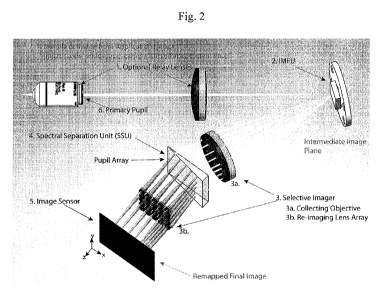
of an example IMS layout is presented in Figure 2. Therein, an optical sample
(not shown) is
imaged by the IMS. The optical sample may be a physical object, an image from
a pre-imaging
system, or a conjugate image of either. The optical sample may provide
electromagnetic
radiation for IMS imaging through any mechanism, such as transmission,
reflection, or
fluorescence. The electromagnetic radiation may be first collected through a
primary pupil 6.
The primary pupil 6 may be preceded and/or followed by one or more optional
relay lenses 1. In
the embodiment shown in Figure 2, an optional relay lens 1 both precedes and
follows the
primary pupil 6. An optional relay lens may be any optical component which is
capable of
relaying an image from the optical sample to the IMFU. For example, an
optional relay lens may
be a lens, an array of lenses, a gradient-index ("GRIN") lens, an optical
fiber or a bundle of
optical fibers. (Fiber optic optional relay lenses may be especially
beneficial in endoscopic
applications.) The electromagnetic radiation then impinges upon the IMFU 2. As
will be
discussed further below, the IMFU 2 spatially reorganizes the image, also
called "image
mapping" or "mapping," as it redirects the electromagnetic radiation towards
the Selective
Imager 3. The IMFU may be located generally at any virtual or real image
conjugate location, or
field space, or within a millimeter or less from an image conjugate location.
The Selective
Imager 3 generally comprises two spatially separated components: (1) a
collecting objective or
array of collecting objectives 3a, and (2) an array of re-imaging lenses 3b.
As shown in Figure 2,
the SSU 4 may be positioned between the two components of the Selective Imager
3. The SSU
may be located generally at any pupil conjugate location, or aperture space,
or within several
millimeters or more from a pupil conjugate location. For example, the SSU 4
may be positioned
between the primary pupil 6, and the IMFU 2, between the IMFU 2 and the
Selective Imager 3,
or between the Selective Imager 3 and the Image Sensor 5. Finally, the
electromagnetic
radiation may impinge upon the Image Sensor 5. The Image Sensor 5 may comprise
any array
of sensing units or detectors capable of quantitatively measuring
electromagnetic radiation, such
as a CCD. It should be understood that, for simplicity, this disclosure may
discuss or illustrate
any given optical component as a lens or a prism, but each component may
comprise multiple
CA 02742273 2011-04-29
WO 2010/053979 12 PCT/US2009/063259
lenses or prisms to achieve the desired effect. As used herein, the
"configuration" of an IMS
generally refers to the number, type, and layout of elements (including the
optical sample,
primary pupil, optional relay lenses, IMFU, Selective Imager collecting
objective, Selective
Imager re-imaging lens array, SSU, and Image Sensor) with respect to one
another.
[0068] An IMFU, or mapper, spatially reorganizes an image to create optically
void regions in the image space used for encoding spectral information. An
IMFU may
comprise optical components spatially distributed on its face. Certain
distributions may exhibit
similar optical functions, thereby forming logical groupings of optical
elements. For example,
mapping regions 1, 4, and 7 may exhibit similar optical functions, and may be
logically grouped
as IMFU optical component group A; while mapping regions 2, 3, 8, and 9 may
exhibit similar
optical functions, different from those in IMFU optical component group A, and
mapping
regions 2, 3, 8, and 9 may be logically grouped as IMFU optical component
group B. In some
embodiments, the IMFU optical component groups may be distributed
symmetrically on the face
of the IMFU. In some embodiments, the distribution of IMFU optical component
groups may
form geometric shapes and/or repeating patterns. The optical components may be
spatially
distributed in particularly useful mapping shapes, such as mapping lines,
mapping pixels, and/or
mapping regions, although other common shapes (e.g., square, triangle, "L",
"0", etc.) may also
be used. The optical components of a particular mapping line, mapping pixel,
and/or mapping
region may, therefore, exhibit similar optical functions specific to that
shape. The distribution of
IMFU optical component groups in other embodiments may be random or chaotic.
The image
created by an optical component group may be referred to as a sub-image. The
particular
distribution of IMFU optical component groups on the face of the IMFU may be
referred to as
the "geometry" of the IMFU. As would be understood by one of ordinary skill in
the art with the
benefit of this disclosure, the geometry of an IMFU uniquely defines the
mapping. Moreover,
the geometry of the IMFU may be static or dynamic, and the geometry may be
controlled and
varied in real-time without disassembly of the system or disturbance of the
optical sample.
[0069] The IMFU optical components may redirect the chief ray from object
points to new locations in the image. The IMFU optical components may be
refractive,
reflective, or waveguide. Refractive approaches may include, for example,
arrays of prisms,
lenses, and/or combination optical components. Reflective approaches may
include, for
example, arrays of mirrors and/or lenses, as in a catadioptric approach.
Waveguide approaches
may include, for example, fiber optics. Any type of mapper also may possess
optical power,
similar to a more traditional field lens or mirror, and may be capable of re-
imaging an exit pupil
CA 02742273 2011-04-29
WO 2010/053979 13 PCT/US2009/063259
from the relay optical system to the Selective Imager collecting objective's
entrance pupil or
array of collecting objective pupils. This may allow for a compact and
optically efficient multi-
imaging system. The mapper may also incorporate anamorphic or cylindrical
curvature for each
mapping component, which may enhance the spectral resolution of the system.
Lastly, the
IMFU may combine refractive and reflective components to perform these
different tasks
individually or in combination. The IMFU may be corrected for spectral
separation.
[0070] Figure 3 shows several examples of possible IMFU designs. For the
purpose of the following discussion, only 9 unique tilt angles are discussed;
however, in practice
many more tilt angles may be used. Additionally, only mirror components are
illustrated, while
IMFU components may also include, for example, prisms, lenses, and combination
optical
components. The geometry in Figure 3(a) illustrates redirection of entire
horizontal mapping
lines through the object into 9 different angular directions. Rotation may be
performed around
two x and y axes to provide large spectral sampling and/or resolution of the
system. This
approach may be advantageous in its simplicity in concept and fabrication.
However, this
approach may suffer in that, for larger tilted mirrors, the image being mapped
may go out of
focus, thereby decreasing the spatial resolution at the edge of the field.
This disadvantage may
be reduced in the second geometry shown in Figure 3(b), wherein the image
mapping line may
be broken into 2, 3, or more segments in the horizontal (x-axis). This
geometry may have better
mapping performance but might be more difficult to fabricate. The third
exemplary IMFU
geometry, shown in Figure 3(c), is a mapping pixel-sized mirror approach,
either static or active
(e.g., MEMS mirrors, liquid crystal modulator, and the like). This concept is
versatile and may
provide any number of remapping schemes for recording both spectral and
spatial information.
Note that mapping pixels do not need to be square or rectangular. An example
of a circular
mapping pixel mapper is illustrated in Figure 3(d) and is conceptually similar
to that shown in
Figure 3(c). In addition to tilted mapping components, each tilt mirror facet
may also have
optical power for focusing the reflected (or refracted) light. This focusing
effect may be used for
compressing the image mapping pixel size, thereby increasing the spectral
sampling of the
system, as shown in Figure 3(e). The entire IMFU may also have optical power
and may be used
for re-imaging the exit pupil of the fore optics in the system, as illustrated
in Figure 3(f). In
Figure 3(g), a combination of two or more element mappers also may be used,
combining tasks
either individually or collectively for image mapping purposes.
[0071 ] As mentioned above, IMFUs may be refractive or reflective. A
refractive
IMFU may be similar in geometry to a reflective IMFU, but a refractive IMFU
may redirect the
CA 02742273 2011-04-29
WO 2010/053979 14 PCT/US2009/063259
optical samples mapping pixel's chief ray as the light is transmitted through,
not reflected from,
the surface. Both refractive and reflective types may be used statically or
dynamically. For
example, dynamic microelectromechanical system ("MEMS") mirror arrays may be
developed
that function similar to a digital light processor ("DLP") device that may be
used in high
definition televisions ("HDTV"). For example, a suitable DLP may be
commercially available
from Texas Instruments of Dallas, Texas. The main drawback of existing DLPs
for this
application is that they are limited to only two possible positions (on and
off), and therefore
cannot provide enough flexibility for real time adjustment of spatial/spectral
resolutions.
Accordingly, an analog or high bit depth array, with several tilt positions in
yaw and pitch to
redirect individual optical sample mapping pixels to any region in the image
plane to maximize
applicability, may be used. Other examples of a dynamic IMFU may also include
liquid crystal
modulators and refractive liquid modulators (micro fluidic based). Such
mappers may be
combined with a tunable refractive or diffractive SSU, like a liquid crystal
modulator or MEMS
based rotating prism and/or array of prisms. The IMS may be used as an
adaptive device capable
of adjusting its spectral and spatial resolution in real-time.
[0072] An IMFU may be fabricated using any available method including, for
example, precision diamond raster flycutting, diamond turning using slow slide
servo, diamond
turning using fast tool servo, micro-diamond milling, precision ruling, CNC
based micro-
grinding and polishing, grayscale lithography based on direct beam writing,
grayscale
lithography using masks, multistep reflow lithography. Diamond machining
approaches may
have several advantages over the other technologies. First, the size, angle,
and relative position
of each optical component may be held very accurately, since it is determined
by precision
numerically controlled stages. Second, complex mapping tilt geometries
(including roll-yaw-
pitch) may be possible with the addition of a precision tilt stage to the
diamond turning lathe.
Third, the initial prototype development cost and time may be less demanding.
And fourth,
precision alignment features may be incorporated into the IMFU, thereby
increasing the
alignment precision of the IMFU with other components, such as baffles and
lens focusing
arrays.
[0073] In particular, an IMFU may be fabricated using diamond raster fly
cutting,
which is an appealing diamond machining method for creating thin, straight,
high aspect ratio
features, such as mirror facets, for the IMFU. As should be understood by one
of ordinary skill
in the art with the benefit of this disclosure, the aspect ratio of an image
is its width divided by
its height. In diamond raster fly cutting, a tool may rotate about a spindle
and scoops material
CA 02742273 2011-04-29
WO 2010/053979 15 PCT/US2009/063259
out of a workpiece (i.e. IMFU), as illustrated in Figure 4(a). For this
example, the workpiece
may traverse the y-axis to create a thin mirror facet. To create adjacent
facets, the workpiece
may step over along the z-axis, as shown in Figure 4(b). This may be repeated
down the length
of the IMFU until the entire surface is cut. Figure 4(b) illustrates a close
up of the tool cutting
the workpiece. Note that the different facet angles may correspond to height
variations in the
workpiece at a specific x-z plane. An example of an IMFU fabricated using
diamond raster
flycutting is shown in Figures 5(a) and 5(c). In some embodiments, a novel
technique may be
applied utilizing surface shaped diamond tools to create the individual
facet's cross section
profile in the IMFU substrate. In traditional raster flycutting, the
individual optical components
comprising the entire mapper may be created by passing a diamond tool across
the mapper
substrate material in both lateral (parallel to mapper surface) and axial
(perpendicular to mapper
surface) directions. With each pass of the tool, a small fraction of the
required material may be
removed. Consequently, multiple passes may be required to fabricate each
optical component,
which leads to an expensive and time consuming process. Fabrication with
surface shaped
diamond tools, on the other hand, may eliminate the need for these lateral
translations, requiring
only axial passes to create the individual (or group) of optical components.
[0074] Moreover, compact, higher sampling (>100 elements) IMFUs may require
much smaller mirror facets. By scaling down the width of the facets, tools
that are pre-shaped
for the cross section profile of the optical component may be used. This may
have several
advantages, including a significant reduction in fabrication time, program
simplicity, more
densely packed mirror facets, and high relative geometric accuracy independent
of machine
precision for axes perpendicular to the cutting direction.
[0075] The disadvantage of this approach is that there may be little ability
to
correct for errors in the cross section of the mirror facet due to the tool
shape, chips, and/or other
defects. This may make the quality of the diamond tools a critical component
in the fabrication
process. An example of a surface shaped fabrication tool is shown in Figures
4(b) and 4(d). In
addition to the tool shown, more complex geometries with multiple facets
and/or features are
also possible and, in some cases, advantageous to a single surface shaped
tool. Figure 5
illustrates an example of a surface shaped tool with 6 facets integrated into
the surface. This
method may be advantageous for fabrication of complex IMFUs as it (1)
decreases the
fabrication time, (2) allows for multi-axis tilts, (3) enables densely packed
features, and (4) is
independent of the precision of the diamond machine for the axis parallel to
the cutting direction.
CA 02742273 2011-04-29
WO 2010/053979 16 PCT/US2009/063259
[0076] There are several design parameters that may be considered for the
surface
shaped diamond tools, such as: included angle 0, primary side clearance angle
a, primary tip
clearance angle ~, top rake angle (3, tool width, maximum depth of cut, edge
quality, and
material. These geometric parameters are illustrated in Figure 4(b) and 4(d).
The flat bottom
tool tip width and the maximum depth of cut may be the key design parameters
of the tool, as
they are determinative of the optical design of the system. The tool tip width
becomes the width
of the mirror facet, while the maximum depth of cut determines the largest
achievable y-axis tilt.
Proper selection of the other tool parameters may be critical for optimum
cutting performance,
durability, tool manufacturability, and overall cost.
[0077] The geometry of the IMFU is also an important aspect in the fabrication
process. To reduce the effects of edge eating caused by the diamond tool
geometry (included
angle) shown in Figure 6, the optical components may be (1) staggered in the y-
axis, as shown in
Figures 7(a) and 7(b), to minimize the step height difference at the edges,
(2) grouped in the x-
tilts, as shown in Figures 7(c) and 7(d), which decreases the number of facets
that have a step
height difference, and/or (3) orientated in concave x-tilt facet positions, as
shown in Figure 7(e),
which reduces the included angle by the magnitude of the adjacent facet tilt.
[0078] Diffraction effects may be another important aspect of the IMFU design,
especially for large format spatial imaging situations, which typically
require hundreds to
millions of miniature optical components tightly packed together. The most
dominate diffraction
effect is thought to be caused by the width of the facets, which are on the
order of 10's -100's of
microns. In the pupil, this diffraction effect may stretch the geometric
diameter in the axis
conjugate to the width of the facet, as shown in Figure 8(a), creating an
elliptical pupil. This
diffraction induced elliptical pupil has a two fold effect on the system.
First, it may lead to
crosstalk. Crosstalk generally refers to the phenomenon that occurs when light
from one sub-
image from the IMFU enters into the optical path of another sub-image. The
IMFU optical
component group creating the first sub-image may be adjacent to the optical
component group
creating the second sub-image. Crosstalk typically occurs at adjacent pupils,
collective
objectives, and/or re-imaging lenses and often leads to degradation of the
final image For -1%
crosstalk, the minimum separation tilt angle should be approximately a,% = f
1. b 35 where
b
A, is the wavelength of light, and b is the width of the facet. This crosstalk
may be verified
theoretically, as shown in Figure 8(b). Note that the pupil distance can
change depending on
other factors associated with the IMFU, such as facet cross section, surface
roughness, and the
CA 02742273 2011-04-29
WO 2010/053979 17 PCT/US2009/063259
incident diffraction limited spot size to name a few. The pupil spacing is
typically, but not
always, related to the spacing of the collecting objectives and/or the re-
imaging lenses of the
Selective Imager, as it is often axially symmetric with at least one of the
Selective Imager
elements. Second, the elliptical pupil may create a "super resolution" effect
in the spectral
domain. As used herein, "super resolution" generally refers to situations
where it is possible to
distinguish an image of one point source from an adjacent one closer than the
Rayleigh criterion.
It should be understood that the Rayleigh criterion is the generally accepted
criterion for the
minimum resolvable features where the first diffraction minimum of an image of
one point
source coincides with the maximum of an adjacent point.
[0079] For large format IMS systems, it is often important to maintain optics
limited, or close-to optics limited, imaging resolution. For Nyquist sampling,
which is the
generally accepted minimum resolvable criteria, at least two IMFU optical
components must
reside within the incident diffraction limited spot to be able to resolve it.
Therefore, the
individual optical components for the IMFU may range in width from
approximately half the
width of the incident diffraction limited spot size to a few spot sizes. The
diffraction limited spot
size may be commonly referred to as the aberration-free image of an
infinitesimal point from the
optical sample.
[0080] An elliptical pupil may create an asymmetric point spread function with
a
narrower axis in the spectral direction perpendicular to the spatial
direction. This effect may be
seen in Figure 9 for an IMFU with 285 facets that are 70 microns wide. The
facets are arranged
for 25 multi-axis tilts (5 x-tilts, 5 y-tilts). Figure 9(a) shows the raw
image of an actual pupil
array. For comparison purposes, a theoretical pupil array image is shown in
Figure 9(b). Cross
section profiles in both the y- and x-axis for both images are compared in
Figure 9(c) and 9(d),
respectively. For the y-axis (Figure 9(c)), the theoretical and measured pupil
diameters and
positions may have excellent agreement. However, in the x-axis (Figure 9(d)),
the measured
pupil diameters may be much larger than expected based on the simulation due
to additional
optical power for each mirror facet in the IMFU. This leads to the second
method to increase the
spectral resolution of the IMS system.
[0081] To enhance the spectral resolution of the IMS, the IMFU individual
optical components may have optical power for compressing the reflected
mapping line widths
smaller than the actual components themselves. Alternatively, a separate array
of optical
components may be added before or after the IMFU to create this optical power.
This optical
power may be used to narrow the width of the mapping line smaller than the
actual IMFU
CA 02742273 2011-04-29
WO 2010/053979 18 PCT/US2009/063259
component, creating additional optical space between adjacent mapping lines
for added spectral
spread, thereby increasing the spectral resolution of the system. In addition,
IMFU optical power
may be used to re-image the entrance pupil from the relay optics to the
entrance pupil of a
Selective Imager collecting objective or array of collecting objectives,
creating a more compact
and optically efficient IMS design.
[0082] The SSU generally is responsible for the spectral separation of the
optical
sample. It may be composed of either a refractive, diffractive, or combination
optical
components. Examples of such components may include wedges, prisms,
diffraction grating,
grisms (a combination of a prism and grating arranged to keep light at a
chosen central
wavelength undeviated as it passes through a camera), computed generated
holograms, and the
like. The SSU may be located in any optical space after the IMFU, although it
is preferable to be
located at the pupil position of the Selective Imager because, among other
things, light from all
field points will illuminate the same region of the component providing more
uniform chromatic
separation. The dispersion direction, or directions, may be in any orientation
except for the
primary mapping axis of the image mapping field unit. If dispersion takes
place in the mapping
axis, then the chromatic and spatial information may be lost or diminished.
The SSU may be
composed of either one continuous optical component over the entire pupil
space or an array of
smaller optical components. Different SSU designs might be as simple as an
optical component
giving spectral separation identical for each object point or differentiate
between these points.
They can be designed as a single SSU optical component or an array of such
optical components.
Both passive and active components are possible. Active components might be
built using liquid
crystal modulators (tunable prisms, wedges, diffraction grating, computer-
generated holograms
("CGHs"), arrays of wedges having adjustable tilts and wedge angles (possibly
MEMS based),
electro-optical modulators, magneto-optical components, or a combination of
gratings giving
different grating constants with changing mutual grating angles. It also may
be advantageous to
design active or passive prisms with either uniform dispersion and/or zero
displacement like that
used in direct vision prisms (i.e. Amici type), as this may allow for a more
compact, evenly
sampled spectral design.
[0083] The Selective Imager works in combination with the IMFU and SSU to
rearrange and reimage the dispersed object onto the Image Sensor. As mentioned
above, the
optical sample may be reorganized spatially and spectrally by the IMFU and
SSU, respectively.
IMS configurations may include a number of possible Selective Imager types and
positions,
including (a) optical systems to selectively separate each sub-image, (b)
optical systems to
CA 02742273 2011-04-29
WO 2010/053979 19 PCT/US2009/063259
selectively separate each tilt direction, and (c) mixed designs having a
number of imagers
between the total number of mapping angles.
[0084] Some embodiments provide IMS configurations having an array of
Selective Imager re-imaging optical systems to match the same number of
optical component
groups and/or mapping tilt directions from the IMFU geometry. The advantage of
this solution
is flexibility of providing various spacing between object zones, but it also
may be complex in
design and possibly require anamorphic optics for asymmetric mapping
geometries. Such
methods may be best suited for certain mapper geometries, such as those
presented in Figure 3(c)
and 3(d), as well as for tunable/dynamic IMS embodiments. Examples of
fabricated Selective
Imager re-imaging lens arrays are shown in Figure 10. The lens arrays may be
composed of a
single achromatized doublet lens or several lenses, such as that shown in
Figures 10 (b) and 10
(c). The Selective Imager may be corrected for chromatic aberrations, as shown
in Figure 11,
with spot diagrams and modulation transfer function plots for the F (-486 nm),
d (587.6 nm) ,
and C (656.3 nm) bands. The design may be diffraction limited at these visible
wavelengths.
The spectral spread introduced by the SSU unit is around 800 microns, as shown
in Figure 12,
for various field positions. Mapping aberrations due to distortion also may be
minimized,
however, since the image may be remapped for display purposes. This may not be
of critical
importance. For alignment purposes, each sub system may have adjustable focus,
either static or
dynamic. Possible dynamic optical components may include, for example, MEMS,
electro-
wetted, micro-fluidic, and liquid crystal lenses, to name a few.
[0085] Other embodiments may provide IMS configurations having an array of
optical systems, wherein the number of mapping angles may correspond to the
number of
required separation pixels for the spectral spread, as illustrated in Figure
13. Note, however, that
this correlation is not necessarily one-to-one, as the spectral spread may be
tilted to cover more
pixels than the number of mapping angles, but it should still be a linear
relationship. The
mapping optical components may be repeated down the IMFU until the entire
image is covered.
In Figure 13, for example, there are 9 unique tilt angles that are then
repeated down the y axis.
[0086] The magnitude and direction of the IMFU mirror tilt angles may
determine where the light from each image mapping line will be directed in the
stop, and
likewise the intermediate pupil. The number of different mirror tilt angles
may be directly
proportional to the number of pupil sub regions. In the example shown in
Figure 13, there are 9
tilt angles and, therefore, 9 pupil sub regions. Behind these sub regions may
be an array of
optical systems that re-image the light from each tilt mirror pupil sub region
onto an Image
CA 02742273 2011-04-29
WO 2010/053979 20 PCT/US2009/063259
Sensor (CCD or other array detector). Each lens may have a field of view
("FOV") of the entire
optical sample but may only receive light from a particular mapping angle.
Consequently, there
may be a large dark region separating the image mapping lines (or, for more
complex mappings,
separating mapping line portions or mapping pixels). A SSU may be placed at
the intermediate
pupil position to disperse the light from each image mapping region or mapping
line into an
angle that will correspond to these dark regions. The final image on the Image
Sensor may look
similar to the diagram in Figure 13(c).
[0087] A simple software algorithm may re-map the optical sample as well as
the
spectral information for each object mapping pixel. Re-mapping might also be
performed in
hardware, for example using a digital signal processing ("DSP") unit. Both
software and
hardware solutions may allow real time display of the 3D (x, y, 2) datacube on
a monitor screen.
In some embodiments, it may be possible for the Image Sensor to comprise
multiple detectors
corresponding to one or more mapping angles, instead of a single, large format
detector. Thus,
using Figure 13 as an example, a large format camera, or 9 low resolution
cameras, or any
number between assuring that all mapping angles are imaged, may be used. Using
multiple
cameras may be implemented to increase spatial and spectral resolution,
minimize unused areas
between images, or in applications like infrared ("IR") where large format
detectors are
generally very expensive or not readily available. A single component Image
Sensor may make
the system more compact, provide a more uniform response, and simplify the
image acquisition.
[0088] In certain embodiments, the IMS may comprise a single tilt axis IMFU.
This may be useful to, among other things, decrease the total number of
components in the
Selective Imager and limit the number of mapping angles, while still providing
sufficient
separation for spectral spread. For example, the IMFU may only require a few
tilts in one
direction (around y axis) and, using a slit or pinhole mask in an intermediate
image plane, may
achieve more separation at the Image Sensor. In other embodiments, increased
separation may
be achieved by using arrays of spherical or cylindrical reimaging systems.
Systems utilizing the
arrays of lenses may require an asymmetric shape which may result in an
asymmetric point
spread function. To compensate, these systems may require an anamorphic relay
imaging
system. An example of such a unidirectional tilt mapper is shown in Figure 14.
[0089] As mentioned above, the IMS may be reflective. Examples of reflective
IMS systems are presented in Figure 15 through 17. Figure 15 illustrates a
reflective system
with tilted annular mirror. Figure 16 shows a reflective IMS with beam
splitter, and in Figure
17, a reflective IMS with a tilted IMFU is shown. In these systems, any choice
of SSU as
CA 02742273 2011-04-29
WO 2010/053979 21 PCT/US2009/063259
described above may be used. In addition, the Selective Imager might have many
different
configurations, for example, consisting of a single collimating objective and
array of re-imaging
objectives or an array of collimators with an array of re-imaging objectives.
The number of
array components may also change depending on the design approach and selected
critical
component configurations.
[0090] One specific example IMS configuration of the present disclosure is a
reflective system with annular mirror. This embodiment of the IMS generally
maintains high
optical throughput with a reflective image mapping field unit. This may be
accomplished by
placing an annular fold mirror at the stop position between objective I and
the collecting
objective (see Figure 15). Light rays from the optical sample (located at the
field stop) may be
imaged by objective 1, passing unobscured through a small, central opening in
the annular mirror
that serves as the stop for that objective. These light rays (depicted by
black lines) may be
imaged onto the IMFU by the collecting objective. The image may be "mapped"
into horizontal
sub mapping regions by tilted rectangular mirrors, for example, as illustrated
in Figure 13. Each
mirror may be the entire length of the image but only one mapping pixel in
width. The different
mirror angles may be repeated down the IMFU until the entire image is covered.
In Figure 13,
there are 9 unique tilt angles that are then repeated down the y axis. Light
reflected from these
mirrors (depicted by colored lines in Figure 15) may travel back through the
collecting objective,
but to the annular mirror region outside of the first objective's stop. The
annular mirror surface
may act as the stop for the collecting objective (L2), and may reflect light
out of the path of the
original system toward a pupil relay. Note that the collecting objective and
re-imaging lens array
form the Selective Imager.
[0091] The pupil relay placed between the collecting objective and the re-
imaging
lens array may image the annular mirror (stop) to a more accessible
intermediate pupil location
while adding the appropriate magnification for fitting the final image onto an
Image Sensor. The
magnitude and direction of the mapping mirror tilt angles may determine where
the light from
corresponding image mapping line will be directed in the stop or its conjugate
intermediate pupil
location. The number of different mapping angles may be directly proportional
to the number of
pupil sub regions. An array of lenses may re-image the light from each sub-
pupil of a particular
mapping sub region onto an Image Sensor, such as a CCD detector or other array
detectors.
Each lens may have a FOV of the entire optical sample, but each may only
receive light from a
particular mapping angle. A SSU may be placed at the Selective Imager stop or
its conjugate
CA 02742273 2011-04-29
WO 2010/053979 22 PCT/US2009/063259
pupil position to disperse the light from each mapping line or mapping region
into an angle that
will correspond to these dark regions.
[0092] This above described system may have the following slight modifications
while still maintaining its overall functionality. The annular mirror may be
faceted to deviate
some of the mapped light into different directions out of the path of the
original system. The
annular mirror may have the unobscured region located at any position on the
surface although
the central region is preferable. The mirror surface does not have to be flat,
but may have some
optical power associated with it. The collecting objective may be arrayed to
accept unique (or a
few) mapping angles. The pupil relay also may be arrayed and/or made
anamorphic for
compression of the spatial data. The SSU also may be a single or array of
systems. The SSU
may be a refractive, diffractive, and/or combination component. The lens array
may be made
anamorphic. The annular mirror may have the SSU placed on its surface or close
to the surface.
[0093] Another specific example of an IMS configuration of the present
disclosure is a reflective IMS with beam splitter. This reflective IMS with
beam splitter may
consist of two optical paths connected by a beam splitter. One is called the
"re-imaging" optical
path (composed of L0, LI, L2, L3, and IMFU), and the other is called the
"mapping" optical
path (composed of IMFU, L3, L2, L4, array of L5 optical systems, SSU, and
Image Sensor).
One embodiment of the system is depicted in Figure 16. Therein, the IMFU
reflects light into N
= 25 different pupils, but any number can be used. The size of the void region
on the Image
Sensor may be proportional to N. The apertures of the L0, L3, and L5 array are
conjugated by
image relay systems. A dispersive prism may be placed at the entrance pupils
of the L5 array to
spread the spectrum from the mapping line from the optical sample, thereby
functioning as the
SSU. After passing through L3, L2, L4, and L5, the image of the optical sample
may be
mapped; the beams may be collimated, dispersed, and re-imaged. In effect, an
image may be
mapped onto the Image Sensor in a pattern of mapping lines dispersed over the
detector area.
Each x, y, and 2 component may be directly mapped to a different camera pixel.
The imaging
system may be telecentric in both object space and image space, providing
lower sensitivity to
defocus. Unfortunately, this setup may be quite energy inefficient, and it may
lose up to about
75% of light (due to two passes at a 50% beam splitter). Its biggest advantage
may be simplicity
and symmetry, which may allow an easy use of entire Image Sensor array.
[0094] Another specific example of an IMS of the present disclosure is a
Reflective and Tilted IMS. One such IMS system is illustrated in Figure 17,
consisting of
optional relay lens, the IMFU, array of collimating lenses, a blazed
diffraction grating, array of
CA 02742273 2011-04-29
WO 2010/053979 23 PCT/US2009/063259
re-imaging objectives, and an Image Sensor located in the image plane. Note
that the diffraction
grating rulings lie parallel to the plane of the page of this document, so the
dispersive effect is
not seen in the cross-section presented. The IMFU modeled here has four tilted
facets (mapping
lines) located on different image heights. It may enable re-organization of
the image into
mapping lines along the x direction separated by multiple mapping pixel rows,
as illustrated in
Figure 17. The diffraction grating may spread these mapping lines in the y-
direction, which may
enable both spatial and spectral information to be recorded simultaneously
without scanning.
One advantage of this system is that it avoids light losses by a beam
splitter. Its biggest
disadvantage may be a tilt of the mapping component, which may increase result
some IMFU
regions being out-of-focus. This may be compensated by tilting an
object/intermediate image to
optimize conjugate planes.
[0095] As mentioned above, the IMS may be refractive. Such IMSs are similar in
concept to the reflective systems, except the IMFU may be a refractive
component instead of
being reflective. One advantage of such IMSs is the fact that the system can
remain unfolded,
making the opto-mechanics less complicated and more compact. Refraction
effects may also
introduce some undesired dispersion, creating spectral separation. As should
be understood by
one of ordinary skill in the art with the benefit of this disclosure, spectral
separation during
mapping may cause neighboring image point to overlap in the final image,
obscuring the
information, and requiring image processing correction. This may compromise
one of the main
advantages of the IMS system: direct unambiguous data acquisition for real-
time image display.
Therefore, it may be advantageous for the refractive optical components in the
IMFU to be
corrected for this spectral separation and other chromatic aberrations. This
can be done a
number of ways, including, but not limited to: combining two or more
refractive materials with
different dispersion, combining a refractive and reflective component, and
combining a
diffractive and refractive component. Light from the optical sample may be
relayed onto the
IMFU by Relay Optics LI (for example, as illustrated in Figure 18). The image
may be
"mapped" into many sub regions or individual mapping pixels by tiny prisms.
These prisms may
have different angles associated with them and may cause the light to travel
along different
paths, as shown in Figure 18 by the different colors. The different optical
paths from the
"mapped" image may be collected by Objective L2 and directed to specific sub
regions in the
pupil. The SSU may disperse the light in these sub regions into different
angles that correspond
to the dark regions created by the IMFU in the final image. Immediately
following the SSU, an
array of lenses may re-image the light onto an Image Sensor (e.g., CCD, CMOS,
or similar
CA 02742273 2011-04-29
WO 2010/053979 24 PCT/US2009/063259
detector), where a simple software algorithm can re-map the optical sample
with its spectral
information.
[0096] This above described system may have the following slight modifications
while still maintaining its overall functionality. Objective 2 may be arrayed
to accept unique (or
a few) mapping angles. The spectral separation unit also may be a single or
array of systems.
The spectral separation unit may be a refractive or diffractive component. The
lens array may be
made anamorphic for spectral or spatial information compression.
[0097] Another approach to certain IMSs of the present disclosure is based on
the
application of an "array of lenses" located such that the field stop coincides
with the focal plane
of lenses. Such IMS configurations may use reflective and refractive
approaches. The micro
lens array may play the role of a parallel sampling probe. Figure 19
illustrates this concept. The
overall imaging principle remains the same, and the IMS may be supplemented
with other
components similar to those used in the layouts presented above. The spatial
resolution of the
system in this case may be determined by the packing density of lenses in the
array, since each
lens may be responsible for a single image point. Light rays launched from the
field stop may
emerge parallel to the optical axis after passing the micro lenses. On
reflection at the mapper,
the optical rays may propagate into specific directions to achieve the
required image mapping.
One advantage of this approach is its insensitivity to defocus. The system's
accuracy may rely
on the uniformity of lenses in the array and quality of beam collimation.
[0098] To capture a greater quantity and/or quality of spectral information, a
dichroic mirror may be added to the image space of the Selective Imager, as
shown in Figure 20.
The dichroic mirror may enable the system to collect spectral information from
the optical
sample in two or more distinct spectral bands, including adjacent spectral
bands, such as visible
and near infrared, and non adjacent spectral bands, such as ultraviolet and
midwave infrared. In
addition, the spectral information also may be enhanced within a single
spectral band, increasing
the spectral resolution by two or more times the original system. The
configuration illustrated in
Figure 20 may utilize an additional camera (Image Sensor detector #2) to
collect the second band
of information. In this diagram, Image Sensor detector #1 may collect light
from the red to green
region of the visible band, and Image Sensor detector #2 may collect light
from green to UV.
However, this concept also may be applied to a single camera Image Sensor in
which filters of
selected wavelength regions are placed in front of rows of neighboring
detector pixels as
illustrated in Figure 21. The unfiltered Image Sensor detector may only spread
spectrum from
one mapping line from the optical sample (line #1) to the next mapping line
from the optical
CA 02742273 2011-04-29
WO 2010/053979 25 PCT/US2009/063259
sample (line #2), as shown in Figure 21(a). For this example, there is no room
for the Blue-UV
spectrum from line #1. By adding filters (for example, see Figure 21(b)) to
the Image Sensor
and oversampling the point spread function of the image, it may be possible to
obtain the
additional spectrum from line 2 (for example, see Figure 21(c)). The tradeoff
with this approach
is that the optical throughput of the system may be decreased. This may be
overcome with lens
arrays similar to those already used in CCD and CMOS image detector to
overcome fill factor
issues.
[0099] Another IMS configuration may use micro lens arrays and/or micro field
stop arrays to optically compress the facets on the mapper, creating
additional space for
spectrum. One possible embodiment is illustrated in Figure 22. In this
example, a set of micro
cylindrical lens arrays are placed near the sub-image plane after the
Selective Imager. The lens
array and/or micro stop array may add additional optical power in the sagittal
plane of the image,
but not the meridonal plane. This may create an asymmetric point spread
function on the final
image plane that is narrower in the sagittal plan, which is also the direction
used for spectrally
spreading the image.
[00]00] A dynamic IMS system is presented in Figure 23. This system has the
ability to act like a digital and optical zoom camera system for the entire 3D
(x, y, 2) datacube,
changing IMS configuration during operation to obtain different spatial and
spectral sampling
from one or multiple mapping regions of the optical sample. It may be possible
to zoom into one
or more regions of interest ("ROI") and obtained higher spectral and spatial
resolution. As used
herein, "zoom" generally refers to increasing the number of samples over a ROI
of an image of
the optical sample. Digital zoom may be an electronic reconfiguring of the
array of sensors
comprising the Image Sensor to change the number of samples in selected
regions of the Image
Sensor. Optical zoom generally means hardware reconfigurations, whereby the
image of the
optical sample is altered to change its sampling by the Image Sensor. Spectral
zoom generally
means increasing the number of sensing elements over a given spectral range,
or decreasing the
spectral range over a given number of sensing elements. Spatial zoom generally
means
increasing the number of sensing elements over a given spatial mapping region,
or decreasing the
spatial mapping region over a given number of sensing elements. This may be
accomplished by
utilizing dynamic components for one or more of the critical components of the
system: IMFU,
SSU, Selective Imager, and, optionally, the image relay lens. The relay lens
may change the size
of an image of the optical sample, increasing the image sampling on the IMFU,
and thereby
zooming the spatial domain. If multiple IMFUs and/or dynamic relay lenses are
used, similar to
CA 02742273 2011-04-29
WO 2010/053979 26 PCT/US2009/063259
Figure 25, it may be possible to provide optical zoom to for more than one
location on the image.
The dynamic IMFU may use MEMS techniques to adjust mirror tilts to selectively
reflect image
mapping pixels of interests toward the Selective Imager, creating zoom in
spectral and spatial
domain. These mapping pixels may then be spectral spread more or less by
dynamically
adjusting the dispersion of the SSU. One possible approach for adjusting the
spectral spread of
the SSU is to use a piano-convex and piano-concave lens pair or similar
materials to create a
prism like structure (for example, see Figure 23). By rotating the piano-
convex lens, the angle of
the prism may change, causing the dispersion of the prism to change as well.
The last
component that can dynamically change is the lens array in the Selective
Imager. By adjusting
the power of the lens array, the final image size also may scale, creating
increased sampling of
the image both spectrally and spatially. This may also make it possible to
image faster (by
binning the camera) and/or improve dynamic range.
[00101] As an alternative to the previously mentioned refractive or reflective
approaches, the IMS system may use a waveguide mapper to create an optically
void region
between adjacent image points, as shown in Figure 24(a). The relay optics
(primary pupil and
zero, one, or more optional relay lenses) image the optical sample onto the
input face of the
waveguide mapper. As shown in Figure 24(b), the waveguide mapper may guide
light from each
individual waveguide to an isolated mapping pixel at the output of the mapper
face. Note that
this mapping may be coherent or incoherent between the mapper input end and
output end. The
mapper face may be imaged by a large FOV objective (L2), dispersed by the SSU,
and imaged
by the re-imaging lens onto an Image Sensor, such as a CCD detector. This
configuration may
utilize a less complicated Selective Imager than the refractive and reflection
components,
however, it may have lower optical throughput due to the cladding around each
waveguide
structure.
[00102] Another embodiment of an IMS system includes two or more IMFU
elements that are imaged onto each other. In other words, they are image
conjugates of each
other. This multiple IMFU conjugate configuration is shown in Figure 25. In
this design, the
optical sample may be imaged on the first IMFU through the optional relay
lenses. This relay
system is optional, as the optical sample may be imaged directly onto the
first IMFU with any
fore optics. The first IMFU may be imaged onto the second IMFU by the IMFU
relay lens.
There may be multiple IMFU relay lens and multiple IMFUs, either sequentially
cascaded one
after another or in parallel, forming and array of IMFUs and relay lenses. The
array approach
may be beneficial for keeping the system compact. For Figure 25, only two
IMFUs are shown
CA 02742273 2011-04-29
WO 2010/053979 27 PCT/US2009/063259
for simplicity, not limitation of the design concept. After the last IMFU (the
second IMFU in
Figure 25) and Selective Imager, the SSU and Image Sensor function in a
similar way as the
prior concepts for example Figure 18. The IMFUs in this design may be either
static or dynamic
or a combination. This type of IMS system may be advantageous in dynamic
systems (Figure
23), allowing for the first component to select one or more ROIs from the
optical sample, and
direct these ROIs to the second IMFU for higher sampling and mapping to one or
more Image
Sensor detectors. This approach also may be capable of simplifying the design
of each IMFU
with each conjugate IMFU responsible for only one aspect of the final mapping.
For instance,
the first IMFU may be responsible for tilts in the x-axis, while the second
IMFU may be
responsible for tilts in the y-axis. This implies that each IMFU for this
embodiment does not
have to have the same geometry or function as the other IMFUs, and each IMFU
may act
independently or dependently.
[00103] As mentioned earlier, the IMS may be adapted for many various
applications. For example, the IMS may be particularly well suited for
endoscopy. An
endoscope version of the IMS concept is illustrated in Figure 26. Discussion
of the IMS system
operation begins at the tissue (distal) side of the coherent multi-fiber
bundle ("MFB"), where a
broadband source may illuminates an area of the tissue (either macroscopic or
microscopic in
size) which becomes our optical sample. Other endoscopic imaging components
also may be
used in substitution or addition to the MFB presented in Figure 26. These
endoscopic imaging
components may include: incoherent fiber bundle, miniature objective,
miniature lenses and grin
lenses. Reflected and/or fluorescent light from the tissue may be collected
and imaged through a
miniature objective onto the MFB distal tip and then transferred to the
proximal end. The image
relay system may magnify and re-image the tissue image from the MFB proximal
face onto the
IMFU. For this illustration, the IMFU may be composed of an array of mirror
facets with
dimensions that correspond to I x 200 mapping pixels at the image plane. Note
that the IMFU
also may be composed of an array of prisms, lenses, and/or a combination of
components. Each
mirror facet may deviate a portion of the tissue image (optical sample) to a
particular region in
the pupil of the Selective Imager (shown by different ray colors). The light
may be spectrally
separated (i.e. dispersed) in the pupil by a SSU (i.e. prism array) into a
range of angles in a plane
different in direction then the mapping plane. A re-imaging lens array may
image each sub-
region onto an Image Sensor. Each sub-image may contain spatial and spectral
information for a
set of mapping regions. Finally, through simple software remapping, the sub
images may be
recombined to form an "unmapped" image of the optical sample (tissue) while
preserving the
CA 02742273 2011-04-29
WO 2010/053979 28 PCT/US2009/063259
spectral signature for each mapping region. Since there is no scanning or
image processing, the
system may acquire and display hyper-spectral images in real time which is
important for
endoscopy applications.
[00104] Ophthalmologists have long relied on optical devices for evaluation of
various eye conditions and diseases. Of particular importance is imaging the
retina of the eye,
which is located at the back inner surface of the eye and contains the light
sensitive
photoreceptors for converting the optical signals to signals that can be
processed by the brain.
Retinal observation and image capture requires the use of a complex optical
device, called a
Fundus camera, which is capable of illuminating and imaging the retina
simultaneously. There
are two main types of Fundus camera designs that vary based on the
illumination system, either
external or internal illumination. The incident illumination provided by
either type is scattered
by the retina and then captured by the imager portion of the Fundus camera
where it can be
viewed by the ophthalmologist directly and/or captured by an image sensing
device.
Ophthalmologists are increasingly using digital detectors such as CCD or CMOS
cameras to
record a picture of the retina. These digital pictures can be used to identify
certain illnesses as
well as track their development over the lifetime of the patient. In this
context, an IMS system
may become an important imaging tool for ophthalmology, where it can obtain a
3D (x, y, k)
image of the retina with additional diagnostic information contained in the
spectrum from each
mapping pixel within the image. Figure 27 shows an example of an IMS system
that is
incorporated into a Fundus camera. The IMS system is positioned at the
sideport or camera port
of the Fundus camera where an image of the retina is located. The IMS system
also may be used
as a standalone system for imaging the eye. For a standalone IMS system, the
illumination may
be integrated into the IMS system, either external or internal to the system
in a similar fashion to
that commonly used in Fundus cameras. The main advantage of an IMS system for
ophthalmic
applications is that the IMS system may collect its 3D datacube in a true
parallel fashion for
quick real-time imaging. This may be important for mitigating any temporal
ambiguities due to
involuntary eye movements. The parallel acquisition may also decrease the
intensity of
illumination, since the collected signal from every image point is integrated
at the same time,
making it is less irritating for the patient's eye. The simple software image
remapping needed
for the IMS system may also allow for real-time feedback for the
ophthalmologist, helping to
direct the examination and provide better quality diagnostic information.
CA 02742273 2011-04-29
WO 2010/053979 29 PCT/US2009/063259
[00105] To facilitate a better understanding of the present invention, the
following
examples of specific embodiments are given. In no way should the following
examples be read
to limit or define the entire scope of the invention.
EXAMPLES
[00106] A working bench top prototype IMS and prototype of a mapping element
(or mapper, Image Mapping Field Unit, or "IMFU") were assembled, configured as
a reflective
Image Mapping Spectrometer ("IMS") with beam splitter. A schematic of the
prototype system
and a picture of the actual setup are presented in Figure 28.
[00107] The optical sample for this IMS configuration came from an inverted
microscope, namely, an Axio Observer Al or AX10, commercially available from
Carl Zeiss,
Inc. For demonstration purposes, the Selective Imager lens array was replaced
with a single lens
(low magnification microscope objective) and was moved to different pupil
locations to image
the corresponding tilt angle field of views ("FOVs"). The IMFU prototype was
fabricated using
raster fly cutting in high purity aluminum. The mapping element had 5 tilt
angles in one
direction only (175 ramp mirrors total). To fabricate the IMFU, a Nanotech 250
UPL Diamond
Turning Lathe was used. The cutting process was lengthy for the first optical
component, as it
took about 120 hours. Once the desired mapping element has been made, it may
be mass
produced either by replication or molding processes (e.g., injection molding,
stamp molding,
etc.) to make it more affordable.
[00108] Figure 29(a) shows the first prototype IMFU. The individual optical
component facets have further been characterized to verify angles and surface
quality using a
white light interferometer, a NewView 5000, commercially available from Zygo
Corporation, as
shown in Figure 29(c). Baffles may be added in front and to the sides of the
mapping element to
reduce scattered light from the transitions mapping optical components. Lens
arrays may also be
added to the mapper to help reduce scattered light by focusing it away from
the edges of the
mapper's optical component and more to the center of the surface of mapping
optical
components. Lens arrays also may reduce the effects of neighboring IMFU
optical component
shadowing. This is especially important at the edges of the optical
components, where the height
differences may be the largest. Although the prototype IMFU was made using
diamond fly
cutting technology, it also may be produced using other technologies, like
diamond milling and
grayscale lithography, depending on the desired geometry. Grayscale
lithography is an
alternative technology for mass producing this element, but it may require
significant process
development time and cost in the initial development stage.
CA 02742273 2011-04-29
WO 2010/053979 30 PCT/US2009/063259
[00109] Figure 30 shows initial imaging experiments performed with the system
prototype. Figure 30(a) shows an image of a 1951 USAF resolution test target
for the central
FOV. Only one mapping direction is demonstrated in the figure and no
dispersion was
introduced in this case. Figure 30(b) shows an image of the Selective Imager
pupil when the
IMS is imaging the output from a single mode (2 630nm) fiber laser (object)
onto at least five
mapping lines of the image mapper. In this example, each mapping line of the
IMFU is
generally a miniature ramp mirror that may be able to reflect a single
(possibly discontinuous)
line of the incident image into a unique direction. The five bright regions
correspond to light
from the object reflected from the different line optical components and their
corresponding
angles. Diffraction and stray light effects caused by the linear IMFU geometry
and surface
roughness account for the light intensity outside of these central regions.
When the re-imaging
lens is moved from one pupil position to the next, the resulting image is
similar to the one shown
in Figure 30(a) but for a different set of linear mappings.
[00110] Figure 30(c) presents an image taken with the prototype system (minus
the
IMFU and the SSU) of a fiber optic illuminated with a halogen light source.
This polychromatic
image is composed of a broad spectral band and represents a typical image one
would obtain
from a standard imaging system. This image typically would appear as a white
circle, and all of
the spectral information would be lost. In this image, there are some blue and
red outer bands in
the image due to lateral chromatic aberrations which may be corrected in the
final system. When
the prototype system is reconfigured to include IMFU and the SSU, the full
spectral signature of
this polychromatic image may be obtained. This is illustrated in Figure 30(d)
for a set of ramp
mirrors with identical tilt angles. As one can see with the spectral data for
the image, mapping
lines may be dispersed into the void regions between the neighboring mirrors -
mapping
components (repeated red to green regions). To reconstruct the final image,
the re-imaging lens
may be translated to the other pupil positions to capture images of the other
mapping lines, and
simple image processing may be done to reconstruct the original image with its
spectral
signature.
[00111 ] A second working prototype IMS was constructed to demonstrate its
ability to obtain fluorescence microscope images. The IMS could obtain a 3D
(x, y, k) datacube
of 100 x 100 x 25 sampling, which corresponds to about 0.45 microns and about
5.6 rim
resolution in spatial and spectral domains respectively. The IMS system was
coupled to an
AX10 inverted microscope, commercially available from Carl Zeiss, Inc., as the
fore optics. A
photograph of the prototype system is shown in Figure 31(a), and the schematic
layout is
CA 02742273 2011-04-29
WO 2010/053979 J 1 PCT/US2009/063259
presented in Figure 31(b). Specimens were placed on the microscope stage and
illuminated by a
120W X-cite`" arc lamp, commercially available from EXFO Life Sciences &
Industrial
Division. The fluorescent signal was collected by an EC Plan-Neofluar,
commercially available
from Carl Zeiss, Inc., 40 x /N.A. - 0.75 objective. The intermediate image was
formed outside
of the microscope side image port, co-located at the field stop of the IMS
system. The
intermediate image at the field stop was first re-imaged by an about 10 x
magnification image
relay system (telecentric both in object and image space) onto a custom-
fabricated image IMFU.
One role of this image relay system is to preserve the image resolution by
matching the size of
image PSF with that of IMFU. The other is to provide strict telecentricity at
the side of IMFU,
which provides correct guidance of chief rays. The IMFU was a one-dimensional
mirror array
that had 25 different two-dimensional tilt angles (0 , 0.23 , 0.46 with
respect to both x and
y-axes), and which could reflect zones of mapped image into 25 different
directions. The total
number of mapping optical components on the IMFU was 100, and each one had
dimensions of
about 16 mm x about 160 m in length and width respectively. In Figure 31(b),
only tilt angles
with respect to the y-axis are shown. The redirected light was gathered by the
collecting lens
(about 130 mm Tube lens, commercially available from Carl Zeiss, Inc., N.A. -
0.033, FOV .,. 25
mm), and formed 25 separate pupils at the pupil plane. An about 5.56 x beam
expander,
commercially available from Edmund Optics (Gold Series Telecentric Lenses
58258, FOV ,,, 8
mm), adjusted the pupil dimensions to match those of the re-imaging lens array
optics. The
magnified pupils were dispersed by a custom prism, SF4, about 10 wedge angle,
commercially
made by Tower Optics, and re-imaged onto a large format CCD camera (Apogee
U16M, 4096 x
4096 pixels, about 9 microns pixel size, RMS noise: 10.5 e-, Dark current:
0.13 e-/pixels) by a
5x5 array of reimaging systems. Each re-imaging lens was composed of an about
60 mm F.L.
positive achromatic doublet (Edmund Optics 47698, dia - 6.25 mm) and an about
12.5 mm F.L.
negative achromatic doublet (Edmund Optics 45420, dia,,. 6.25 mm) to form a
long focal length
lens (F.L. - 350mm). Note that the IMS prototype presented here does not use
the full CCD
resolution. However, this large Image Sensor may allow improved resolution of
the system
resolution in future system development.
[00112] The format of the final image may be very important for maximizing the
mapping of the 3D (x, y, 2) datacube onto the recording 2D Image Sensor. In
many cases, it is
advantageous for each detector, or pixel, on the Image Sensor to record a
signal from the optical
sample. For unambiguous data collection, each voxel in the datacube may
correspond to about
one pixel on the Image Sensor. Unambiguous mapping that efficiently utilizes
all of, or a large
CA 02742273 2011-04-29
WO 2010/053979 J2 PCT/US2009/063259
number of, the available detectors in the Image Sensor may require the sub-
images from the
IMFU to be in close proximity to each other. Note that in the majority of
configurations, the
Image Sensor may have more than one sub-image of the IMFU. To correct for
fabrication
errors, optical aberrations, stray light, other unaccounted for fabrication
errors, and optical
effects, the IMFU geometry may provide for some distance between adjacent sub-
images.
Ideally, this unused Image Sensor surface area should be no greater than about
40% of the total
detecting surface area. On the other hand, it may also be beneficial for the
sub-images to overlap
to include both ambiguous and unambiguous data, which may improve the
available spectral and
spatial content of the system. This overlap may be as small as a few detectors
on the Image
Sensor, and may range up to every detector on the Image Sensor. As previously
mentioned, the
disadvantage of too much sub-image overlap is that software reconstruction
algorithms may
become quite time consuming, eliminating the ability of the IMS to display
data in real-time. It
also may be advantageous for the sub-images of the final mapped image to be
arranged to match
industry standard camera formats and aspect ratios like those listed in Table
1, although custom
formats also may be used.
Table 1: Image sensor formats
Aspect Width Height Diagonal
Imager Format Ratio (mm) (mm) (mm)
1/4 in. 4:3 3.2 2.4 4
1/3 in. 4:3 4.8 3.6 6
1/2 in. 4:3 6.4 4.8 8
2/3 in. 4:3 8.8 6.6 11
1 in. 4:3 12.8 9.6 16
4/3 in. 4:3 17.8 13.4 22.3
APS 3:2 25.1 16.7 30.1
35 mm 3:2 36.0 24.0 43.3
48 x 36 mm 4:3 48.0 36.0 60.0
645 4:3 56.0 41.5 69.7
10.5 / 16.8 MP 1:1 36.8 36.8 52.1
4.3 MP 1:1 50.02 50.02 70.7
[00113] The listed dimensions in Table 1 are approximate, as each Image Sensor
manufacturer varies slightly. Some of the most common aspect ratios may be
1:1, 3:2, and 4:3
CA 02742273 2011-04-29
WO 2010/053979 J3 PCT/US2009/063259
[00114] The FOV of the reimaging lens set in this prototype IMS was designed
to
be overlapped with adjacent lens sets to maximize the usable area of the CCD
camera. As the
whole IMFU plate's image had a square shape, while the FOV of the reimaging
lens set was
circular, four void regions outside the IMFU plate's image but inside the FOV
existed (see
Figure 32). Because of these void regions, the FOV of neighboring reimaging
lens sets were
allowed to overlap. This allowed a fully utilized imaging area on the CCD
camera. The CCD
camera used a 10.5 / 16.8 MP format chip comprising 16 megapixels within a
square (36.8 x
36.8 mm) surface area.
[00115] To verify the image performance and test the spatial and spectral
resolution of the IMS prototype, an undispersed 1951 USAF resolution test
target was imaged,
and the point spread function ("PSF") of a single image mapping line (from
single mirror
mapping component) was measured. Spectra images of test samples made with
fluorescent
beads were obtained. The results are shown in Figures 33-36.
[00116] A third prototype IMS was constructed to demonstrate a large format
configuration capable of collecting a 3D (x, y, 2) datacube of 285 X 285 X 62
for fluorescence
specimens. The layout of the IMS configuration is similar to the 2nd prototype
and is shown in
Figure 37. This IMS configuration represents major technology advancements in
a large format
IMFU. The IMFU had densely packed mirror facet optical components that are
only about 70
microns wide, enabling 285 facets to reside within the FOV of the relay
optics. Due to the small
size of the facets, diffraction effects had to be considered in the design,
and additional tilt angles
were applied to minimize crosstalk between sub-imaging systems. Lastly, the
IMFU geometry
was optimized to reduce edge eating effects and improve system throughput.
[00117] The biological imaging capability of the third prototype was evaluated
by
imaging bovine pulmonary artery endothelial cells incubated with MitoTracker
Red CMXRos to
label the mitochondria, BODIPY FL phallacidin to label the filamentous actin
(F-actin), and
DAPI to label the nucleus. A reference image taken with a color CCD camera is
shown at the
top left corner of Figure 38 for comparison purposes. The lower sequence of
images was taken
with an IMS system in a single, about 4 sec integration event. A sample of 25
spectral images
are display over an about 505 to about 684 nm spectral range, with an average
sampling of about
5 nm. Spectrally encoded features within the cell are easily identifiable and
show a strong
correlation with the reference image.
[00118] To manufacture IMFUs with a variety of geometries, three different
surface shaped tool designs have been developed. Table 2 lists the different
design
CA 02742273 2011-04-29
WO 2010/053979 34 PCT/US2009/063259
specifications for each surface shaped tool. Tool 41 was the first surface
shaped tool used to
fabricate the 100 component IMFU used in the IMS fluorescence hyperspectral
microscope
shown in Figure 31. This surface shaped tool has an about 160 micron wide flat
bottom tip and
was used to create a square shaped IMFU with a side length of about 16 mm.
Tool #2, an about
75 micron flat bottom surface shaped tool, was developed for the larger format
IMS system,
shown in Figure 37, which still resides within the FOV constraint of the
collecting objective.
This surface shaped tool increases the spatial sampling to a 250 component
IMFU. Tool #3 is
also about 75 microns wide, but it has a reduced included angle to minimize
the effects of edge
eating.
Table 2 - Surface Shaped Flat Bottom Tool Design Parameters
Parameter Tool #1 Tool #2 Tool#3
Included Angle, 0, (deg) 20 0.5 20 0.5 5 0.5
Side clearance angle, a (deg) 3 3 3
Tip clearance angle, 4 (deg) 6 5 5
Top rake angle, (3 (deg) 0 0 0
Tool Tip Width, (pm) 150 15 70 7 70 7
Max. Depth of Cut, ( m) 500 300 300
Edge quality 750 X 750 X 750 X
Material (Diamond) Synthetic Synthetic Synthetic
[00119] For fabrication of the IMFUs, a high precision CNC 4-axis diamond
lathe
(Nanotech 250UPL) was used. This machine has about 200 mm of travel for each
axis (x, y, z)
with nanometer level precision. The workpiece was mounted on two stages, with
y and z axis
movement, while the spindle and diamond tool were mounted on the x axis stage
see Figure
39(a). The mirror optical component facets were cut by moving the workpiece up
and down in
the y axis. Tilts in the y direction were achieved by moving in both the x and
y directions while
cutting each mapping line optical component. After cutting a mapping line
optical component,
the spindle and tool moves away from the workpiece, rewinds, and begins
cutting the next
mapping line optical component. The workpiece also steps over in the z axis by
the tool width
prior to cutting the next mapping line optical component. The x-tilts were
obtained by mounting
the workpiece to a goniometer (Newport P/N: GON40-U with manual high
resolution
micrometer P/N: HR-13) with its cutting surface coincident with the
goniometers axis of rotation
(see Figure 39(b)). Due to the manual rotation of the goniometer, x-tilts were
fabricated at the
CA 02742273 2011-04-29
WO 2010/053979 J5 PCT/US2009/063259
same time. When finished, the goniometer is adjusted to the next x-tilt, and
the process is
repeated until all mirror optical component facets are fabricated. Y height
compensation factors
were applied for the different x-tilts. For large x-tilt angles, z-axis
compensation factors also
may be used to compensate for the cosine effect.
[00120] To manufacture an IMFU optical component, in general, a rough cut is
performed initially to get the different mirror facets into the aluminum
substrate. The substrate
also may be made out of any other diamond machinable material, such as those
listed in Table 3.
After this step, a fine cutting program is used to clean up the IMFU optical
component,
producing the best surface roughness and removing cosmetic imperfections, such
as metal flaps,
chips, and other debris.
Table 3 - Possible IMFU substrate Materials
Metals Polymers IR crystals
= Aluminum = Acetyl = Cadmium Sulfide
Alloys = Aclylic = Cesium Iodide
= Brass = Fluoroplastic = Indium Antimonite
= Copper = Nylon = Magnesium Fluoride
= Gold = Polycarbonate = Phosphate (KDP)
= Nickel = Polypropylene = Tellurium Dioxide
= Silver = Polysulfone = Cadmium Telluride
= Tin = Silicone = Gallium Arsenide
= Zinc = Olefin = Iridium
= Zeonex (polyolefin) = Potassium Bromide
= Silicon
= Zinc Selenide
= Calcium Fluoride
= Germanium
= Lithium Niobate
= Potassium Dehydrogenate
= Sodium Chloride
= Zinc Sulfide
[00121] Figure 40(a) shows a picture of the final large format (250
component) IMFU fabricated using tool #3. Figure 40(b) shows a close up side
view of the
CA 02742273 2011-04-29
WO 2010/053979 36 PCT/US2009/063259
IMFU, showing the excellent alignment of the facets. The x-tilt grouping and
concave
orientation are easily observed as well as the staggered y-tilts.
[00122] The mirror optical component facet tilts and widths were measured
using a
white light interferometer (Zygo NewView). Before component testing, the IMFU
was placed
on the interferometer's motorized 4-axis stage (X, Y, Ox, Oy) and adjusted to
align the reflected
light from the zero tilt (x- and y- axis) mirror facet of the IMFU with the
optical axis of the
system. Any residual tilt was recorded and subtracted from the other facet
tilt measurements. A
10X Mirau Objective with a 1.OX field lens (FOV =0.72 mm x 0.54 mm, Res. =
1.12 microns)
was used to collect the data. Ten measurements were taken for each tilt
position and averaged
together. Table 4 shows the final results, comparing the measured values to
the designed tilt
values. The results from this study demonstrate an excellent agreement between
the desired tilt
values and those actually measured. The largest tilt error was -2 mrad for the
x-tilt (a2=0.010
rad.), with most of the tilts having no significant error.
Table 4 - Comparison of IMFU tilt designed and measured values
x-tilt y-tilt Ideal Measured Error
(a's) ((3's) (rad.) (a'S) (R's) (a's) (3's)
al 31 +0.020 +0.020 +0.020 0 0
a2 (32 +0.010 +0.098 +0.010 -0.002 0
a3 (33 0 - - - -
a4 (34 -0.010 -0.010 -0.010 0 0
a5 (35 -0.020 -0.021 -0.020 +0.001 0
[00123] The width of each optical component facet was measured by
taking a cross section profile across its surface at the left, center, and
right edge of the facet.
Figure 42 shows typical results obtained from these measurements. During the
fabrication
process, an approximate 5 micron overlap was introduced to remove a thin metal
flap between
adjacent facets. This overlap changes the designed width of the facets from
about 75 microns to
between about 70-65 microns, depending on facet position. For the center x-
tilts (2-4) the
measured widths were within about +/- 1 micron of the 70 microns; however, for
the edge
positioned x-tilts (1 & 5) this changes to about 50-70 microns, depending on
the y-tilt. The
highest mapping line optical component due to the y-tilt will be the thinner
due to this overlap
as well as some edge eating, as shown in the 2D intensity maps in Figure 41.
[00124] The roughness of the mirror optical component facet surfaces reduces
the
final image contrast and throughput of the IMFU. To quantify this effect, a
white light
CA 02742273 2011-04-29
WO 2010/053979 37 PCT/US2009/063259
interferometer with a 50X Mirau Objective, 2.OX field lens (FOV =0.07 mm X
0.05 mm, Res.
0.11 microns) was used. Figure 42 shows a typical roughness result obtained
from a single facet.
For this fabrication method, the tool imperfections create lines along the
length of the facets. To
gain a more statistical estimate of the IMFU's surface roughness, ten randomly
selected facet
surface regions were measured and found to have an average rms roughness of
5.3 +/-1.2 rim.
The optical throughput of the IMFU was estimated to be approximately 97% based
on this
roughness value.
[00125] Notwithstanding that the numerical ranges and parameters setting forth
the
broad scope of the invention are approximations, the numerical values set
forth in the specific
examples are reported as precisely as possible. Any numerical value, however,
inherently
contain certain errors necessarily resulting from the standard deviation found
in their respective
testing measurements.
[00126] Therefore, the present invention is well adapted to attain the ends
and
advantages mentioned as well as those that are inherent therein. While
numerous changes may
be made by those skilled in the art, such changes are encompassed within the
spirit of this
invention as illustrated, in part, by the appended claims.