Note: Descriptions are shown in the official language in which they were submitted.
CA 02742843 2011-05-05
WO 2010/059411 PCT/US2009/062929
1
LED DRIVER WITH SINGLE INVERTER CIRCUIT WITH ISOLATED MULTI-
CHANNEL OUTPUTS
BACKGROUND OF THE DISCLOSURE
[0001 ] Light emitting diode (LED) lighting systems have been gaining
increasing
popularity in replacing incandescent and discharge lamps due to their long
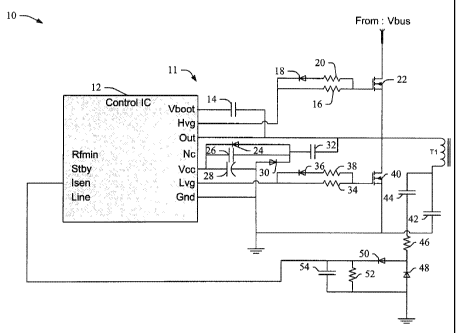
life, energy
efficiency, and flexibility in optical design. As a result, the application of
LED systems
has come to include not only low-power applications, but also high-power
applications.
LED systems are also gaining popularity in outdoor applications, in addition
to indoor
applications. Moreover, LED systems are being used in general applications,
and not
just in special lighting applications.
[0002] For some applications, a Class II isolation for output is required. A
typical Class
II high-power LED driver design uses a common front-end power factor
correction
section with either multiple isolated LED converters in parallel, or with
multiple single
stage isolated LED drivers connected to the same power sources. In such
arrangements,
component redundancy is undesirably high. Consequently, the cost and size of
such
arrangements are high and system efficiency is low.
[0003] Accordingly, there is an unmet need in the art for systems and methods
that
facilitate reducing component redundancy and increasing system efficiency in
Class-II
rated circuits, and for overcoming the deficiencies noted above.
SUMMARY OF THE DISCLOSURE
[0004] In accordance with one aspect, a circuit for controlling an LED
lighting system
comprises a single-converter control circuit with a primary winding Ti, and a
first
isolated output channel circuit with at least one secondary winding T2, T3
tightly
coupled to the primary winding Ti and to a first output current sensing and
conditioning
circuit. The circuit further comprises at least a second isolated output
channel with at
CA 02742843 2011-05-05
WO 2010/059411 PCT/US2009/062929
2
least one secondary winding T6, T7 tightly coupled to the primary winding Ti
and to a
second output current sensing and conditioning circuit. The circuit further
comprises an
output current regulation circuit that determines peak current output through
the first
and second isolated output channels.
[0005] In accordance with another aspect, an LED driver output channel
regulation
circuit comprises a voltage-sensing winding T4 that senses voltage across a
multi-
channel secondary circuit, and at least first and second photodiodes that
transmit
current, the first and second photodiodes being coupled to respective isolated
output
channel circuits in the secondary circuit. The circuit further comprises a
peak current
regulation component that compares current transmitted by the photodiodes,
determines
which of the isolated output channel circuits has a higher peak output
current, and
regulates the output current thereof.
BRIEF DESCRIPTION OF THE DRAWINGS
[0006] FIGURE 1 illustrates a primary side of the circuit, which includes an
IC
controller and a half-bridge-based resonant converter, in accordance with one
or more
aspects described herein.
[0007] FIGURE 2 illustrates a secondary side of the circuit, including
multiple isolated
output channels, in accordance with one or more aspects described herein.
[0008] FIGURE 3 illustrates a current regulation portion of the circuit, which
regulates a
channel having a highest sensed output current at any given time, in
accordance with
one or more aspects described herein.
DETAILED DESCRIPTION OF THE PREFERRED EMBODIMENTS
[0009] The following description relates to a single converter circuit-based
LED driver
with isolated multi-channel outputs. Advantages of the described circuit
design include
that all outputs meet Class II requirements, only one IC control and converter
circuit is
CA 02742843 2011-05-05
WO 2010/059411 PCT/US2009/062929
3
used, component count is reduced, and efficiency is improved. That is, the
single
converter with multiple outputs facilitates providing a circuit at low cost,
high efficiency
and small size. A half-bridge-based resonant converter is employed as a
platform for a
high-power LED driver application. However, it will be appreciated that a
current-fed,
fly-back, or any other isolated circuit platform can be employed in
conjunction with the
various embodiment set forth herein.
[0010] FIGURES 1-3 illustrate a circuit 10 comprising a single converter
circuit-based
LED driver with isolated multi-channel outputs, in accordance with various
aspects
described herein. The following discussion relates to the specific
configuration of the
circuit 10, and features thereof. As shown in FIGURE 1, the circuit 10
comprises a
control integrated circuit (IC) 12, which comprises a plurality of
input/output (I/O) pins.
In one example, the IC 12 is an L6599 IC. A capacitor 14 (e.g., a 0.1 F
capacitor or the
like) is coupled to a bootstrapped supply voltage (Vboot) pin on the control
IC 12, as
well as to a high-side driver reference (Out) pin and a primary transformer
winding Ti.
According to an example, the winding Ti is a G30876 winding. A high-side
driver
output (Hvg) pin on the IC 12 is coupled to a resistor 16 and diode 18, which
in turn is
coupled to a resistor 20. Resistors 16 and 20 are coupled to a gate of a
switch 22 (e.g., a
MOSFET or the like), and the drain of the switch 22 is coupled to a voltage
bus. In one
example, the resistor 16 is a 2052 resistor, the diode 18 is a 1N4148 diode,
the resistor
20 is a 1kQ resistor, and the switch 22 is an IRF740 MOSFET.
[0011] A source voltage (Vcc) pin on the IC 12 is coupled to each of a diode
24, a
capacitor 26, and a capacitor 28. The capacitor 28 is coupled to a diode 30,
which is
coupled to a capacitor 32, as well as to the diode 24, the capacitor 26, and
to ground.
The capacitor 32 is further coupled the diode 24, the capacitor 26, the
capacitor 14, the
output pin on the IC 12, and the primary transformer winding Ti. According to
an
example, the diodes 24 and 30 are 1N4148 diodes, the 26 is a 0.1 F capacitor,
the
capacitor 28 is a 10 F capacitor, and the capacitor 32 is a 150pF capacitor.
[0012] The low-side driver output (Lvg) pin on the IC 12 is coupled to a
resistor 34 and
diode 36, which in turn is coupled to a resistor 38. Resistors 34 and 38 are
coupled to a
gate of a switch 40 (e.g., a MOSFET or the like), and the drain of the switch
40 is
CA 02742843 2011-05-05
WO 2010/059411 PCT/US2009/062929
4
coupled to the source of the switch 22. The source of the switch 40 is coupled
to the
diode 30, the capacitor 28, a capacitor 42, and to ground. The capacitor 42 is
further
coupled to the primary transformer winding Ti and to a capacitor 44. In one
example,
the resistor 34 is a 2052 resistor, the diode 36 is a 1N4148 diode, the
resistor 38 is a 1kQ
resistor, the switch 40 is an IRF740 MOSFET, the capacitor 42 is a 15nF
capacitor, and
the capacitor 44 is a 100pF capacitor.
[0013] The capacitor 44 is coupled to a resistor 46, which is coupled to
diodes 48 and
50. The diode 50 is coupled to a resistor 52 and a capacitor 54, both of which
are
coupled to ground and to the diode 48, which is also coupled to ground. The
diode 50,
the resistor 52, and the capacitor 54 are further coupled to a current sensing
(Isens) pin
on the IC 12. Other pins on the IC (e.g., Nc and Line, etc.) are left
unconnected. A
ground pin on the IC 12 is coupled to the capacitor 28, the diode 30, and to
ground. In
one example, the resistor 46 is a 5052 resistor, diodes 48 and 50 are 1N4148
diodes, the
resistor 52 is a 10kQ resistor, and the capacitor 54 is a 33nF capacitor.
[0014] Turning now to FIGURE 2, with continued reference to Figure 1, the
circuit 10
includes a first isolated output channel 70, a second isolated output channel
72, and an
output current sensing and conditioning circuit 74.
[0015] The first output channel circuit 70 includes the winding T5, which is
coupled to
Earth groundl, as well as to a capacitor 76 and a diode 78. The capacitor 76
and diode
78 are coupled to a diode 80, which in turn is coupled to a capacitor 82. The
capacitor
82 is coupled to the diode 78, the winding T5, and the Earth ground 1. The
circuit
further includes secondary transformer windings T2 and T3, both of which are
coupled
to Earth ground 1 (E-Gnd1), and inductively coupled to winding Ti. In one
example,
the capacitors 76, 82 are 22nF capacitors, the diodes 78, 80 are 1N4148
diodes, and the
windings T2, T3, T5 are G30876 windings.
[0016] Winding T5 is tightly coupled to the primary side windings (e.g., Ti,
T4), and
has a voltage source Vcc3 (e.g., a power supply) that ensures a voltage even
if the
output of channel 1 is shorted.
CA 02742843 2011-05-05
WO 2010/059411 PCT/US2009/062929
[0017] The second output channel circuit 72 includes the transformer windings
T6 and
T7. A diode 84 is coupled to winding T6, as well as to a diode 86 that is
coupled to
winding T7. The diodes 84 and 86 are further coupled to a capacitor 88, which
is
coupled to the windings T6 and T7 and to Earth ground 2 (E-Gnd2). The diodes
84 and
86, and the capacitor 88, are coupled to an output current (lout) sensing and
conditioning component 90 and to an LED 92. The lout sensing and conditioning
circuit 90 (e.g., similar or identical to the output current sensing and
conditioning circuit
74) is coupled to an LED 94. In one example, the diodes 84, 86 are MUR420
diodes,
the capacitor 88 is a 100 F capacitor, and the LEDs are NCSW136 LEDs.
[0018] The circuit 10 further includes a resistor 96 and a resistor 98 that
are coupled to
an amplifier 100. The amplifier 100 is further coupled to a photodiode 102 and
a
resistor 104, which are also coupled to each other. The amplifier 100 is
coupled to a
capacitor 106, which is also coupled to the photodiode 102 and a resistor 108.
The
resistor 108 is coupled to the amplifier 100 and to a resistor 110, which is
in turn
coupled to a resistor 112 and an LED 114. The resistor 112 is additionally
coupled to
Earth ground 1 (E-Gndl). According to an example, the resistor 96 is a l Ok52
resistor,
the resistor 98 is a 1k52 resistor, and the amplifier 100 is a LM325
amplifier. In another
example, the photodiode 102 is am SFH6106 photodiode, the resistor 104 is a
5052
resistor, the capacitor 106 is a 22nF capacitor, the resistor 108 is a 5.6k52
resistor, and
the resistor 110 is a 1k52 resistor. In yet another example, the resistor 112
is a 0.2552
resistor, and the LED 114 is an NCSW136 LED.
[0019] An LED 116 is coupled to a diode 118, a diode 120, and a capacitor 122.
The
diode 118 is coupled to secondary winding T2, and the diode 120 is coupled to
the
secondary winding T3. The diodes 118 and 120 are further coupled to the
capacitor
122, which in turn is coupled to the secondary windings T2 and T3, and to
Earth ground
1 (E-Gndl). According to an example, the LED is an NCSW136 LED, the diodes
118,
120 are MUR420 diodes, and the capacitor 122 is a 100 F capacitor.
[0020] Now turning to FIGURE 3, with continued reference to Figures 1 and 2,
the
circuit 10 includes an output current regulator circuit 128 with a voltage-
sensing
winding T4 that is coupled to a diode 130, which in turn is coupled to a
resistor 132.
CA 02742843 2011-05-05
WO 2010/059411 PCT/US2009/062929
6
Winding T4 is tightly coupled to the secondary windings (e.g., T2, T3, T5, T6,
and T7)
and senses a voltage across the secondary side of the circuit 10 (see Fig. 2).
Output
voltage increases when there is a light load or no-load condition, such as
when one or
more LEDs are not connected. If the output voltage reaches or exceeds a
predetermined
threshold voltage (e.g., approximately 55V or so in one example), then the
circuit 10
switches from current regulation to voltage regulation. Output currents for
all channels
are sensed, and the channel with the highest output current is regulated.
According to an
example, the winding T4 is a G30876 winding, the diode 130 is a 1N4148 diode,
and
the resistor 132 is a 10052 resistor.
[0021] The resistor 132 is coupled to a capacitor 134 and a resistor 136,
which is further
coupled to a capacitor 138. The resistors 132 and 136, and the capacitor 134
are
coupled to a resistor 140 which in turn is coupled to a resistor 142 and to
the winding
T4. The capacitor 134 is coupled to the resistor 136 and to the winding T4, as
well as to
the resistor 142. In one example, the capacitors 134, 138 are 33nF capacitors,
the
resistors 136, 142 are 1kQ resistors, and the resistor 140 is a l0kQ resistor.
[0022] The resistor 142 is further coupled to a resistor 144, which in turn is
coupled to a
voltage source Vcc2. The resistors 142 and 144 are coupled to an error
amplifier 146,
which is also coupled to Vcc2. The capacitor 138 is coupled to a resistor 148,
which is
also coupled to a diode 150. The resistor 148 and diode 150 are coupled to the
error
amplifier 146, and the diode 150 is further coupled to a resistor 152 that is
coupled to a
Standby (Stby) pin on the IC 12. According to an example, the resistor 144 is
a 10kQ
resistor, the amplifier 146 is an LM325 amplifier, the resistor 148 is a 6.2kQ
resistor,
and the diode 150 is a 1N4148 diode. In another example the resistor 152 is a
5kQ
resistor.
[0023] A resistor 154 is coupled to a minimum oscillating frequency setting
(RfMin) pin
on the IC chip 12 and to a peak output current regulating component 156. The
regulating component 156 is further coupled to phototransistors 158 and 160,
which in
turn are coupled to each other and to ground, and which receive current signal
from the
photodiode 102 and equivalent photodiodes in other isolated channels (e.g.,
such as a
second photodiode in the output current sensing and conditioning circuit 90).
According
CA 02742843 2011-05-05
WO 2010/059411 PCT/US2009/062929
7
to an example, the resistor 154 is a 4.7kQ resistor, the current regulating
component 156
is a G20678 component, and the phototransistors 158, 160 are SFH6106
phototransistors.
[0024] Still referring to Figures 1-3, in the main transformer, all isolated
windings are
tightly coupled to each other to ensure that even with unbalanced loads on
each output,
the voltages on each output are equal to each other with minimum error. In
each
channel, the output current is sensed and fed back to the primary side (e.g.,
Figs. 1 and
3) to control and regulate the output current. Although all the outputs'
currents are
sensed, it is the highest current in the outputs that is regulated. The
voltage and current
characteristic of the photodiodes and error amplifiers are used to determine
the other
channel's current. In one embodiment, each channel employs the same type and
numbers of LEDs, which are connected in series with even thermal distribution.
[0025] As shown in the Figures, the two secondary outputs are tightly coupled
together
for matching voltage at the output of each channel. Each channel drives the
same type
and number of LEDs in a series/parallel configuration. On each channel, there
are two
windings, T2 and T3, on secondary outputs with the common tie to the E-Gndl.
The
diodes 118 and 120 are connected to T2 and T3 respectively to charge 122 and
maintain
the energy on the cap 122 and current to the LEDs 114, 116.
[0026] The sensing resistor 112 senses the channel output current, and the
amplifier 100
further conditions the sensed signal and drives cathode of an optocoupler
(which
communicate signal(s) to phototransistors 158, 160). The amplifier 100 has a
non-
inverting input that is connected to a scaled down reference and inverting
input via
resistor 110 connected to sensing resistor 112. The windings T2, T3, which are
tightly
coupled to the primary winding Ti and isolated from the main power converter,
provide
the power supply for the first channel 70. The second channel 72 is configured
the same
as the first channel 70, but isolated by the separated windings T6, T7.
Additional
channels can be added in the same fashion as the second channel 72. Therefore,
all the
channels are isolated from the main power converter to meet Class II
requirements.
[0027] On each channel, the optocoupler feeds back the output current signal
to the peak
current regulator 156. The channel with the highest output current is
regulated at any
CA 02742843 2011-05-05
WO 2010/059411 PCT/US2009/062929
8
given time. In the event that a light load or no load condition is present in
an output
channel, voltage on the winding T4, which is tightly coupled to secondary of
the output
transformer, is indicative of the voltage on the output channels. This voltage
is
processed by error amplifier 146 to take over the control loop to regulate the
maximum
output voltage.
[0028] Accordingly, the circuit 10 facilitates sensing output currents for a
plurality of
isolated output channels and regulating the current of the channel with the
highest
output current at a given time. In this manner, the circuit eliminates a need
to use
multiple Class II converters for LED applications. Thereby saving costs,
reducing
circuit size, and increasing efficiency.
[0029] It will be appreciated that the specific examples of component values
and/or
model numbers presented herein are illustrative in nature and are not to be
interpreted in
a limiting sense. Other component values and/or models may be employed to
achieve
the described circuit functionality, as will be appreciated by those of skill.
[0030] The invention has been described with reference to the preferred
embodiments.
Obviously, modifications and alterations will occur to others upon reading and
understanding the preceding detailed description. It is intended that the
invention be
construed as including all such modifications and alterations.