Note: Descriptions are shown in the official language in which they were submitted.
CA 02743108 2016-08-12
WO 2010/112404
PCT/EP2010/053938
1
MULTI-TOUCH OPTICAL TOUCH PANEL
Field of the Invention
The various embodiments described herein relate to an optical touch panel,
and,
more particularly, to a multi-point optical (e.g. infrared) touch panel.
Background of the Invention
A variety of touch panel technologies are presently in existence, including
resistive technology, capacitive technology, surface acoustical wave (SAW)
technology, infrared (IR) technology, etc. Comparing with other touch panel
technologies, the IR technology has lots of advantages, for example, better
durability, reliability, sealability, and no calibration required etc.
In the case of IR touch panel technology, infrared emitter, collector pairs
are used
to project an invisible grid of light a small distance over the surface of the
panel.
When a beam is interrupted, the absence of the signal at the collector is
detected
and converted to touch coordinates (e.g., X/Y rectangular coordinates). Since
the method of
determining a touch is optical instead of electrical or mechanical, IR
touch panels are not as sensitive to damage as some technologies, such as
resistive
and capacitive technologies.
The construction of a conventional optical touch panel is disclosed in U.S.
Patent No.
6,597,508. Fig. 1 shown in the patent depicts the construction of a
conventional optical
touch panel. The optical touch panel comprises a plurality of light-emitting
elements (e.g.,
LEDs) arranged along two adjacent sides of a rectangular position-detecting
surface and a
plurality of light-receiving elements (e.g., photo transistors) 130 arranged
along the other
two sides of the rectangular position-detecting surface such that the light-
emitting elements
110 are positioned opposite to the respective light-receiving elements
and the position-detecting surface is positioned between the light-emitting
elements and
CA 02743108 2016-08-12
W02010/112404
PCT/EP2010/053938
2
the light-receiving elements. In the optical touch panel, however, the
light-emitting elements and the light-receiving elements must be arranged
along
the four sides of the position-detecting surface, and hence it takes a
significant
amount of time to establish wire connections among the elements. Thus, the
optical touch
panel is complicated, its assembly difficult, and it is difficult to reduce
its size.
Another construction of a conventional optical touch panel is disclosed in
Taiwan
Patent Application No. 96151662.
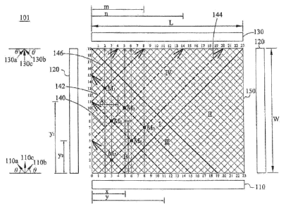
With reference to Fig. 1, a schematic diagram of the construction of an
optical
touch panel 101 shown in the Taiwan patent application No. 96151662 is
provided.
The optical touch panel 101 may comprise a rectangular position-detecting
surface
150 with a specified length L and a specified width W (wherein L may be
greater than or
equal to W), a plurality of light-emitting element pairs (110a, 110b), two
reflectors (e.g.,
mirrors) 120, and a plurality of light-receiving element pairs (130a, 130b).
Each light-
receiving element may be configured for receiving light beams reflected by the
reflectors
120 or light beams directly emitted by the plurality of light-emitting element
pairs without
reflection. The plurality of light-emitting element pairs (110a, 110b) may
comprise light
emitting diodes (LEDs). The plurality of light-receiving element pairs (130a,
130b) may
comprise photo transistors.
The plurality of light-emitting element pairs (110a, 110b) may be arranged in
pair at
various points along a first side 110 of the rectangular position-detecting
surface 150 in a
lengthwise (L) direction. More specifically, there may be various points
(e.g., point 0, point 1
point L) along the first side 110 at which the plurality of light-emitting
element pairs (310a,
310b) may be arranged. At each of these various points, other than the
starting and the
ending points (i.e., point 0 and point L, which are at the edges of the first
side 110), a first
light-emitting element (110a) and a second light-emitting element (110b) may
be arranged
in pair [note that at the starting point (i.e., point 0), a second light-
emitting element (110b)
may be arranged, while at the ending point (i.e., point L), a first light-
emitting element
(110a) may
CA 02743108 2011-05-09
WO 2010/112404
PCT/EP2010/053938
3
be arranged]. The first light-emitting element (110a) may be arranged at the
left side of each
light-emitting element pair (110a, 110b) at an angle 180-0 with reference to
the first side
110, and the second light-emitting element (110b) may be arranged at the right
side of each
light-emitting element pair (110a, 110b) at an angle 0 with reference to the
first side 110. The
angle 0 with reference to the first side 310 may be greater than an angle 13,
which may be the
angle of the diagonal line of the rectangular position-detecting surface 150
with reference to
the x-axis of the rectangular position-detecting surface 150. According to the
exemplary
embodiment of the Taiwan patent application No. 96151662, the angle 0 may be
45
degrees, in which case the angle between the first light-emitting element
(110a)
and the second light-emitting element (110b) of each light-emitting element
pair
(110a, 110b) is 90 degrees.
Similarly, the plurality of light-receiving element pairs (130a, 130b) may be
arranged in pair at various points along a second side 130 opposite to the
first side
110 of the rectangular position-detecting surface 150 in the lengthwise (L)
direction. More specifically, there may be various points (e.g., point 0,
point 1 ... point L)
along the second side 130 at which the plurality of light-receiving element
pairs (130a,
130b) may be arranged. At each of these various points, other than the
starting and
the ending points (i.e., point 0 and point L, which are at the edges of the
second side 130),
a first light-receiving element (130a) and a second light-receiving element
(130b)
may be arranged in pair [note that at the starting point (i.e., point 0), a
second light-
receiving element (130b) may be arranged, while at the ending point (i.e.,
point L), a first
light-receiving element (130a) may be arranged]. The first light-receiving
element
(130a) may be arranged at the left side of each light-receiving element pair
(130a,
130b) at an angle 0-180 with reference to second side 130, and the second
light-
receiving element (130b) may be arranged at the right side of each light-
receiving
element pair (130a, 130b) at an angle ¨0 with reference to the second side
130. The
angle 0 with reference to the second side 130 may be greater than the angle 0.
According to
an exemplary embodiment, the angle 0 may be 45 degrees, in which case the
angle
between the first light-receiving element (130a) and the second light-
receiving
element (130b) of each light-receiving element pair (130a, 130b) is 90
degrees.
CA 02743108 2011-05-09
WO 2010/112404
PCT/EP2010/053938
4
The two reflectors 120 may be arranged along two opposing sides of the
rectangular position-detecting surface 150 in a widthwise (W) direction for
reflecting light beams emitted by the plurality of light-emitting element
pairs
(110a, 110b).
In accordance with the exemplary embodiment as shown in Fig. 1A, given L=23
and W=19, each of the second light-receiving elements (130b) at points 0
through
4 may receive light beams emitted from the first light-emitting elements
(110a) at
points 19 through 23 respectively. Moreover, each of the first light-receiving
elements
(130a) at points 19 through 23 may receive light beams emitted from the second
light-
emitting elements (110b) at points 0 through 4 respectively. It is important
to note that such
transmissions of light beams are not explicitly illustrated in Fig. lA but
nevertheless are
possible with respect to the optical touch panel 101 as depicted in Fig. 1A.
A control circuit (not shown) may be configured for causing the light-emitting
element pairs
(110a, 110b) to emit light beams in a predetermined order for the purpose of
scanning the
position-detecting surface 150. For instance, the light-emitting element pairs
(110a, 110b)
may emit light beams one-by-one in a sequential order from left to right, or a
plurality of
alternate light-emitting element pairs may simultaneously emit light beams at
a given time.
Moreover, the control circuit may be configured for causing the plurality of
light-receiving
element pairs (130a, 130b) to receive the light beams emitted from the
plurality of light-
emitting element pairs (110a, 110b). Accordingly, optical paths may be formed
on the
position-detecting surface 150 in a grid pattern as shown in Fig. 1A.
When an object Mo (e.g., a pointing device such as a touch pin or a finger) is
positioned on the position- detecting surface 150 as shown in Fig. 1A, the
object
M blocks a light beam 140 emitted by one of the first light-emitting elements
(110a) and reflected by one of the reflectors 120. Moreover, the object M
blocks a
light beam 142 directly emitted by another of the first light-emitting
elements
(110a).
CA 02743108 2011-05-09
WO 2010/112404
PCT/EP2010/053938
Due to the blockage of the light beam 140 and the light beam 142, two of the
light-receiving elements do not receive these light beams. The two light-
receiving
elements that do not receive the light beams may be located at two points that
respectively may be a distance 'm' and 'n' away from the left edge (i.e.,
point 0)
5 of the second side 130 of the rectangular position-detecting surface 150.
Accordingly, one of the two light-receiving elements not receiving a light
beam may be "at a
left portion" of the second side 330 and accordingly may be positioned at the
point that is
'm' away from the left edge, while the other of the two light-receiving
elements not
receiving a light beam may be "at a right portion" of the second side 330 and
accordingly
may be positioned at the point that is 'n' away from the left edge. Similarly,
the two
light-emitting elements that correspond to the two light-receiving elements
may be
located at two points that respectively may be a distance 'x' and 'y' away
from the
left edge (i.e., point 0) of the first side 110 of the rectangular position-
detecting
surface 150.
Accordingly, the control circuit may be configured to determine the X/Y
rectangular coordinates (A, B) of the object Mo based on which light-receiving
elements fail to receive a light beam during a scan cycle due to blockage of
the
light beam 140 and the light beam 142.
If the object Mo blocks more than two light beams, the coordinates of the
intended
center position of the object Mo may be determined by averaging the detected
coordinate information. Such averaging may be completed by the control circuit
or
by another device operatively coupled to the optical touch panel 101.
In accordance with the exemplary embodiment of the Taiwan patent application
No. 96151662, in order to determine the X/Y rectangular coordinates of the
object
Mo positioned on the position-detecting surface 150 in the event that the
object Mo
blocks two light beams, the control circuit may be configured for dividing the
position- detecting surface 150 into four regions I, II, III, and IV. These
four
regions I, II, III, and IV may be based on whether each of the two light-
receiving
elements not receiving a light beam is a first light-receiving element 130a or
a
CA 02743108 2011-05-09
WO 2010/112404
PCT/EP2010/053938
6
second light-receiving element 130b of one of the plurality of light-receiving
element pairs (130a, 130b). Since the length `L' and the width 'W' of the
position-
detecting surface 150 and the positions of two of the light-receiving elements
that
do not receive the light beams may be given, equations to determine the X/Y
rectangular coordinates (A, B) of the object Mo respectively for the four
regions I,
II, III, and IV via geometric analysis can be obtained.
The problem for the optical touch panel 101 mentioned above will be only
single
point detected. For example, when a user simultaneously touches two points, M2
and M4, on the position-detecting surface 150, the control circuit cannot
determine
the actual X/Y rectangular coordinates of points M2 and M4. The points M2 and
M4
block four light beams, respectively as light beam 140, 142, 144 and 146. In
such
case, there will be six potential points (i.e. Mo, M1, M2, M3, M4, MO being
obtained
via the computation of the equations mentioned above based on the blocked
light
beam 140, 142, 144 and 146. Therefore, there exist potential combinations of
other two points that block the same four light beams, e.g. points (Mi and M5)
or
(Mo and M3). Accordingly, the control circuit cannot determine the actual X/Y
rectangular coordinates of points M2 and M4 based on which light-receiving
elements fail to receive a light beam during a scan cycle due to blockage of
the
light beams, such as the light beams 140, 142, 144, 146. These points except
points M2 and M4 are not actual points and thus are defined as phantom points.
However, there are many applications requiring "multi-point" touch in order to
provide users more friendly user interface and better interaction between
people
and machine, for example, Apple iPod0 Touch which provides a friendly
multi-point touch interface or called a multi-touch interface. Additionally,
although multi-point touch is a very attractive technology, only other touch
panels
are built in the "multi-point" touch technology. In the technical field of
optical
touch panel, there has not been the feature of the "multi-point" touch being
integrated thereto. Accordingly, it would be advantageous to integrate a
feature of
the "multi-point" touch with an optical touch panel.
CA 02743108 2011-05-09
WO 2010/112404
PCT/EP2010/053938
7
Summary of the Invention
One aspect of the present invention discloses a multi-touch optical touch
panel
which comprises a position-detecting surface with a specified length and a
specified width. Moreover, the multi-touch optical touch panel may comprise a
first set of plurality of light-emitting element pairs configured for emitting
a
plurality of light beams, wherein the first set of plurality of light-emitting
element
pairs are arranged in pair at various points along a first side of the
position-
detecting surface in a lengthwise direction. A first light-emitting element
may be
arranged at the left side of each light-emitting element pair at an angle 180-
0i with
reference to the first side, and a second light-emitting element may be
arranged at
the right side of each light-emitting element pair at an angle Oi with
reference to
the first side.
Additionally, a second set of plurality of light- emitting elements may be
arranged
at said various points along the first side at 90 degrees with reference to
the first
side. The optical touch panel may comprise two reflectors (e.g. mirrors)
arranged
along two opposed sides of the position-detecting surface in the widthwise
direction, wherein the reflectors are configured for reflecting the plurality
of light
beams emitted by the first set of plurality of light-emitting element pairs.
Furthermore, the optical touch panel may comprise a first set of plurality of
light-
receiving element pairs configured for receiving the plurality of light beams
emitted by the first set of plurality of light-emitting element pairs, wherein
the
first set of plurality of light-receiving element pairs are arranged in pair
at various
points along a second side of the position- detecting surface opposite to the
first
side in a lengthwise direction. A first light-receiving element is arranged at
the
left side of each light-receiving element pair at an angle Oi-180 with
reference to
the second side, and a second light-receiving element is arranged at the right
side
of each light-receiving element pair at an angle -01 with reference to the
second
side.
CA 02743108 2011-05-09
WO 2010/112404
PCT/EP2010/053938
8
A second set of plurality of light-receiving elements are arranged at said
various
points along the second side at -90 degrees with reference to the second side
for
receiving the plurality of light beams emitted by the second set of plurality
of
light-emitting elements.
The optical touch panel may comprise a control circuit which is configured for
causing the first set of plurality of light-emitting element pairs and the
second set
of plurality of light-emitting elements to emit the plurality of light beams
in a
predetermined order to scan the position-detecting surface, and further
configured
for causing the first set of plurality of light-receiving element pairs and
the second
set of plurality of light-receiving elements to receive the plurality of light
beams,
thereby forming optical paths on the position-detecting surface in a grid
pattern.
The multi-touch optical touch panel is adapted for detecting objects
positioned on
the position-detecting surface, and wherein at least a portion of the
plurality of
light beams are blocked by the objects when the objects are positioned on the
position-detecting surface, thereby hindering the portion of the plurality of
light
beams from reaching one of the second set of plurality of light-receiving
elements
and at least one of the first or second light-receiving elements of at least
one of
the first set of plurality of light-receiving element pairs.
Another aspect of the present invention discloses a method of determining
actual
coordinates of objects positioned on a position-detecting surface of a multi-
touch
optical touch panel, comprising: detecting, for angle 0i, all light-receiving
elements that do not receive light beams during a scan cycle due to the
blockage
of the light beams by objects and the distances of the light-receiving
elements
away from the left edge of the rectangular position-detecting surface;
obtaining all
potential combinations by selecting any two of all light-receiving elements
that do
not receive the light beams in order to determine all potential positions of
objects,
and separately computing touch coordinates of all potential positions of
objects to
create a set of the coordinates of objects; repeating the previous steps for
next 0i;
and retrieving an intersection from all sets of coordinates of all potential
positions
CA 02743108 2011-05-09
WO 2010/112404
PCT/EP2010/053938
9
of objects created for different angle Oi in order to obtain the actual
coordinates of
objects, after all computations for all Oi are finished.
Still another aspect of the present invention discloses a method of arranging
a first
set and a third set of plurality of light-emitting element pairs and a second
set of
plurality of light-emitting elements on a frame-shaped circuit board that
surrounds the
perimeter of a position-detecting surface, comprising: arranging the first set
of
plurality of light-emitting element pairs on a first surface of the frame-
shaped circuit board
in pair at various points along a first side of the position-detecting surface
in a
lengthwise direction, in which a first light-emitting element is arranged at
the left
side of each of the first set of light-emitting element pairs at an angle 180-
01 with
reference to a first side, and a second light-emitting element is arranged at
the
right side of each of the first set of light-emitting element pairs at an
angle Oi with
reference to the first side; arranging the third set of plurality of light-
emitting element
pairs on a second surface of the frame-shaped circuit board in pair at various
points
along the first side of the position-detecting surface in the lengthwise
direction, in
which a first light-emitting element is arranged at the left side of each of
the third
set of light-emitting element pairs at an angle 180-02 with reference to the
first
side, and a second light-emitting element is arranged at the right side of
each of
the third set of light-emitting element pairs at an angle 02 with reference to
the
first side; and arranging the second set of plurality of light-emitting
elements on the first
surface of the frame-shaped circuit board, in which each light-emitting
element is
arranged at said various points along the first side at 90 degrees with
reference to
the first side; wherein there does not exist a multiple relationship among the
angle
02, 90 degrees and the angle O.
Brief Description of the Drawings
Embodiments of the invention will next be described, by way of example only,
with reference to the accompanying drawings in which:
CA 02743108 2011-05-09
WO 2010/112404
PCT/EP2010/053938
Fig. 1 is a schematic diagram of the construction of an optical touch panel
101
shown in the Taiwan patent application No. 96151662 (and counterpart US patent
application US 2009/0167724;
5 Fig. 1B is a schematic diagram of the construction of a multi-touch
optical touch
panel formed by improving that of Fig. lA to provide the detection of two-
point
touch;
Fig. 2A and Fig.2B are a schematic diagram of the construction of a multi-
touch
10 optical touch panel solving the problem of Fig. 1B;
Fig. 3 is a schematic diagram of arranging the added plurality of light-
emitting
element pairs (210c, 210d) and the corresponding plurality of light-receiving
element pairs
(230c, 230d) for the construction of a multi-touch optical touch panel
provided for
detecting four-point touch according to one embodiment of the present
invention.
Fig.4 is a top view of arranging the plurality of light-emitting element pairs
(210a, 210b)
according to the construction of a multi-touch optical touch panel provided
for
detecting four-point touch of the present invention;
Fig. 5 is a bottom view of the plurality of light-emitting element pairs
(210c, 210d, 210e)
according to the construction of a multi-touch optical touch panel provided
for
detecting four-point touch of the present invention;
Fig. 6 is a side view of the multi-touch optical touch panel according to the
construction of a multi-touch optical touch panel provided for detecting four-
point
touch of the present invention; and
Fig. 7 is a flowchart of determining actual coordinates of objects or touches
positioned on a position-detecting surface of a multi-touch optical touch
panel
provided for detecting four-point touch.
CA 02743108 2016-08-12
=
MA) 2010/112404 PCT/EP2010/053938
11
Detailed Description
The following describes various exemplary embodiments. The disclosed
embodiments are only for illustration. Thus, it will be understood by those
skilled
in the art that there are many modifications that may be made to the various
embodiments described herein without departing from the scope of the
disclosure. Throughout the drawings, similar features are identified by
similar
reference numerals.
With reference to Fig. 1B, a schematic diagram of the construction of a multi-
touch optical touch panel formed by improving that of Fig. IA to provide the
detection of two-point touch is provided. As illustrated, in addition to the
plurality
of light-emitting element pairs (110a, 110b) and the plurality of light-
receiving element
pairs (130a, 130b) that may be respectively arranged in pair, as shown in Fig.
1A,
at the various points (e.g., point 0, point 1 point L) along the first side
110 of the
rectangular position-detecting surface 150 in a lengthwise (L) direction and
the various
points (e.g., point 0, point 1 point L) along a second side 130 opposite to
the first
side 110, a plurality of light-emitting elements 110c and a plurality of light-
receiving
elements 130c may be further arranged respectively at the first side 110 and
the
second side 130. The plurality of light-emitting elements 110c may be arranged
at the
various points (e.g., point 0, point 1 point L) along the first side 110 at an
angle 90
with reference to the first side 110, while the plurality of light-receiving
elements
130c may be arranged at the various points (e.g., point 0, point 1 point L)
along the
second side 130 at an angle (-90) with reference to the second side 130.
In such situation, as shown in Fig. 1 B, each of the six points (Mo, MI, M2,
M3, M4,
M5) shown in Fig. IA has three light beams passing through during a scan
cycle. If
a user simultaneously touches two points, M2 and M4, on the position-detecting
surface 150, as the aforementioned case, there will be other combinations of
two
30 points selected from the six points (i.e. Mo. MI, M2, M3, M4, M5) that
block the same
four light beams, respectively as light beam 140, 142, 144 and 146, for
example,
points (M1 and M5) or (Mo and M3) mentioned above, but only light-receiving
CA 02743108 2011-05-09
WO 2010/112404
PCT/EP2010/053938
12
elements 130c positioned at point 5 and point 6 fail to receive a light beam
during
a scan cycle due to blockage of the light beams only emitted by the light-
emitting
elements 110c positioned at point 5 and point 6. Accordingly, the control
circuit
may be configured to determine the actual X/Y rectangular coordinates (A, B)
of
the objects M2 and M4 further based on which light-receiving elements 130c
fail
to receive a light beam during a scan cycle due to blockage of the light beams
emitted by the light-emitting elements 110c. Considering the special case only
provided for detecting two-point touch on the position-detecting surface
mentioned above, the present invention may be broadened to determine the
actual
coordinates of (n-1) objects that simultaneously touch (n-1) points if each
point on
the position-detecting surface 150 has (n) light beams passing through during
a
scan cycle.
A control circuit (not shown) may be configured for causing the light-emitting
elements (110a, 110b, 110c) to emit light beams in a predetermined order for
the
purpose of scanning the position-detecting surface 150, and also causing the
light-
receiving elements (130a, 130b, 130c) positioned opposite to the respective
light-
emitting elements to receive the light beams emitted from the light-emitting
element pairs (110a, 110b, 130c). Accordingly, optical paths may be formed on
the
position-detecting surface 150 in a grid pattern to determine the X/Y
rectangular
coordinates of the two touch points.
Now refer back to Fig. 1B, if a user simultaneously touches two points, Mo and
M5, on the position-detecting surface 150, in such case, both point Mo and M5
are
located on the same optical path formed by the light beam emitted by the light-
emitting elements 110c positioned at point 3. The control circuit cannot
determine
which object, Mo or M5, blocks a light beam emitted by the light-emitting
elements
110c positioned at point 3. Accordingly, the construction of an optical touch
panel
shown in Fig. 1B cannot determine the actual X/Y rectangular coordinates of
objects (or touches), when there are "phantom" points presented on the same
optical path formed by the light beam emitted by the light-emitting elements
110c.
The reason that there are "phantom" points presented on the same optical path
is that
CA 02743108 2011-05-09
WO 2010/112404
PCT/EP2010/053938
13
there exists a multiple relationship between the angle 0 (90 degrees) used for
arranging light-emitting element 110c and the angle 0 (45 degrees) used for
arranging the plurality of light- emitting element pairs (110a, 110b) in the
embodiments as illustrated in Fig. lA and Fig. 1B.
With reference to Fig. 2A and Fig.2B, a schematic diagram of the construction
of a
multi-touch optical touch panel solving the problem of Fig. 1B is provided. As
illustrated in Fig. 2A, the plurality of light-emitting element pairs (210a,
210b) may be
arranged in pair at various points (e.g., point 0, point 1 ... point 14) along
a first side
respectively at an angle (180-01) and an angle Oi with reference to the first
side of the
rectangular position-detecting surface 250 in a lengthwise (L) direction,
while the plurality
of light-emitting elements 210e may be arranged at various points (e.g., point
0, point 1 ...
point 14) along the first side at an angle 03 (i.e. 90 degrees) with reference
to the
first side (as shown in Fig. 1B). Similarly, the plurality of light-receiving
element pairs
(230a, 230b) may be arranged in pair at various points (e.g., point 0, point 1
... point 14)
along a second side opposite to the first side respectively at an angle (01-
180) and an
angle (-01) with reference to the second side of the rectangular position-
detecting surface
250 in a lengthwise (L) direction, while the plurality of light-receiving
elements 230e may
be arranged at various points (e.g., point 0, point 1 ... point 14) along the
second side at an
angle -03 (i.e. -90 degrees) with reference to the second side.
Since, there does not exist a multiple relationship between the angle 03 (90
degrees) used for arranging light- emitting element 210e and the angle 01
(which
is not 45 degrees) used for arranging the plurality of light- emitting element
pairs
(210a, 210b) in the embodiments as illustrated in Fig. 2A and Fig. 2B.
Accordingly,
the problem that there are "phantom" points presented on the same optical path
is
solved.
Similar to the aforementioned exemplary embodiment of the Taiwan patent
application No. 96151662, when an object M is positioned on the position-
detecting surface 250 of the optical touch panel as shown in Fig. 2A, the
object M
blocks two light beams, thereby hindering the two light beams from reaching
two
CA 02743108 2011-05-09
WO 2010/112404
PCT/EP2010/053938
14
light-receiving elements positioned opposite to the light-emitting elements. A
control circuit (not shown) may be configured for dividing the position-
detecting
surface 250 into four regions I, II, III, and IV. These four regions I, II,
III, and IV
may be based on whether each of the two light-receiving elements not receiving
a
light beam is a first light-receiving element 230a or a second light-receiving
element 230b of one of the plurality of light-receiving element pairs (230a,
230b).
The angle Oi will not be 45 degrees as disclosed in the exemplary embodiment
of
the Taiwan patent application No. 96151662. However, as previously discussed,
there may be two light-receiving elements that do not receive light beams due
to
blockage by the object M, and these two light-receiving elements may be
located
at two points that are respectively a distance 'm' and 'n' away from the left
edge
of the second side of the position-detecting surface 250 with length '1_,' and
width
'W'. Taking into account the parameters (L, W, m, n, Ai) and the four regions
I, II,
III, and IV of the position-detecting surface 250, the control circuit may be
configured to compute via geometric analysis the X/Y rectangular coordinates
(A,
B) of the object M. Such computation may be carried out through the use of
four
equations, wherein the equation used in a given case depends on which of the
four
regions the object M is located. The X/Y rectangular coordinates (A, B) may be
computed via the following:
If the two light-receiving elements that do not receive a light beam during a
scan
cycle are both first light-receiving elements (230a), then the object M is
positioned within the region I of the position-detecting surface 250. The
equation
to determine the X/Y rectangular coordinates (A, B) when the object M is
positioned within the region I is the following:
( A, B ) = ( I n __________ ¨2m 1 , W _ n+m tanel )
2
If the two light-receiving elements that do not receive a light beam during a
scan
cycle are both second light-receiving elements (230b), then the object M is
CA 02743108 2011-05-09
WO 2010/112404
PCT/EP2010/053938
positioned within the region II of the position-detecting surface 350. The
equation
to determine the X/Y rectangular coordinates (A, B) when the object M is
positioned within the region II is the following:
5 ( A, B) = ( L - In __ -21111, ( W - L tan 01 ) n fil tan 01 )
2
If the light-receiving element at a left portion of the second side of the
position-
detecting surface 250 that does not receive a light beam during a scan cycle
is a
first light-receiving element (230a), and the light-receiving element at a
right
10 portion of the second side of the position-detecting surface 250 that
does not
receive a light beam is a second light-receiving element (230b), then the
object M
is positioned within the region III of the position-detecting surface 250. The
equation to determine the X/Y rectangular coordinates (A, B) when the object M
is
positioned within the region III is the following:
( A, B) = ( L - n+111 , (W L ) 1 n _____________________ ¨2111 1 tan01 )
2
If the light-receiving element at a left portion of the second side of the
position-
detecting surface 250 that does not receive a light beam during a scan cycle
is a
second light-receiving element (230b), and the light-receiving element at a
right
portion of the second side of the position-detecting surface 250 that does not
receive a light beam is a first light-receiving element (230a), then the
object M is
positioned within the region IV of the position-detecting surface 250. The
equation to determine the X/Y rectangular coordinates (A, B) when the object M
is
positioned within the region IV is the following:
( A, B ) = ( n+m,W 1 n-111 1 tan01 )
2 2
CA 02743108 2011-05-09
WO 2010/112404
PCT/EP2010/053938
16
The X/Y rectangular coordinates (A, B) of a 'single' object M may be
determined
uniquely via the computing mentioned above. Fig.2A and Fig.2B are a schematic
diagram of the construction of a multi-touch optical touch panel provided
merely
for two-point touch. If a user simultaneously touches two points on the
position-
detecting surface 250 as shown in Fig. 2A, the two points will block four
light
beams. In such case, there will be six potential points being obtained via the
computation of the equations mentioned above based on the blocked light beam.
According to the rule mentioned above, the actual coordinates of (n-1) objects
that simultaneously touch (n-1) points can be determined if each point on the
position-detecting surface has (n) light beams passing through during a scan
cycle.
Accordingly, the construction of a multi-touch optical touch panel provided
for
detecting four-point touch can be made by further adding other light-emitting
elements and corresponding light- receiving elements on the position-detecting
surface 250 as shown in Fig. 2A and Fig. 2B, in order to obtain six potential
points via the computation of the equations mentioned above based on the
blocked
light beam for extracting the actual touch points and determine the actual
coordinates of objects or touches when requiring four-point touch. Fig. 3 is a
schematic diagram of arranging the added plurality of light-emitting element
pairs
(210c, 210d) and the corresponding plurality of light- receiving element pairs
(230c, 230d)
on the position- detecting surface 250 for the construction of a multi-touch
optical
touch panel provided for detecting four-point touch. The details of how to
arrange
the plurality of light-emitting element pairs (210a, 210b, 210c, 210d) and the
plurality of
light-emitting elements 210e, or the plurality of light-receiving element
pairs (230a, 230b,
230c, 230d) and the plurality light-receiving elements 230e will be described
later with
reference to Fig. 4 to Fig. 7.
As illustrated in Fig. 3, it shows other light-emitting elements and
corresponding
light-receiving elements with an angle 02 other than the angle 01 are added on
the
position-detecting surface 250 as shown in Fig. 2A and Fig.2B that are the
construction of a multi-touch optical touch panel provided for detecting two-
point
touch. The added plurality of light-emitting element pairs (210c, 210d) may be
arranged in
CA 02743108 2011-05-09
WO 2010/112404
PCT/EP2010/053938
17
pair at various points (e.g., point 0, point 1 ... point 14) along a first
side respectively at an
angle (180-02) and an angle 02 with reference to the first side of the
rectangular position-
detecting surface 250 in a lengthwise (L) direction. Similarly, the
corresponding plurality of
light- receiving element pairs (230c, 230d) may be arranged in pair at various
points (e.g.,
point 0, point 1 ... point 14) along a second side opposite to the first side
respectively at
an angle (02-180) and an angle (-02) with reference to the second side of the
rectangular
position- detecting surface 250 in a lengthwise (L) direction. There does not
exist a
multiple relationship among the angle 02, the angle 03 (90 degrees) used for
arranging light-emitting element 210e and the angle 01 (which is not 45
degrees)
used for arranging the plurality of light-emitting element pairs (210a, 210b)
in the
embodiments as illustrated in Fig. 2A and Fig. 2B. That is, the angle 02 is
also not 45
degrees. Accordingly, there will be not "phantom" points presented on the same
optical path. In such situation, the construction of the multi-touch optical
touch
panel by integrating Fig. 2A, Fig. 2B and Fig. 3 may used to identify four
objects
that simultaneously touch four points, and determine actual coordinates
thereof.
The details of how to determine will be described later with reference to Fig.
7.
Fig. 4, Fig. 5 and Fig. 6 respectively show an assembled perspective view of
how
to arrange the plurality of light-emitting element pairs (210a, 210b, 210c,
210d) and the
plurality of light-emitting elements 210e, or the plurality of light-receiving
element pairs
(230a, 230b, 230c, 230d) and the plurality light-receiving elements 230e in
accordance
with the multi-touch optical touch panel of the present invention provided for
detecting
four-point touch, in which Fig.4 is a top view of arranging the plurality of
light-emitting
element pairs (210a, 210b), Fig. 5 is a bottom view of the plurality of light-
emitting element
pairs and the plurality of light-emitting elements (210c, 210d, 210e), and
Fig. 6 is a side
view of the multi-touch optical touch panel. As shown in Fig. 6, the plurality
of light-
receiving element pairs (210a, 210b) and the plurality of light- receiving
element pairs
(210c, 210d) may be respectively arranged on the top side and bottom side of
the
position-detecting surface 250. The plurality of light-receiving element
pairs, the
plurality of light-emitting elements, the plurality of light-receiving element
pairs and the
plurality of light-receiving elements are affixed to a frame-shaped circuit
board 310 that
surrounds the perimeter of the position- detecting surface 250.
CA 02743108 2011-05-09
WO 2010/112404
PCT/EP2010/053938
18
Fig. 7 is a flowchart of determining actual coordinates of objects or touches
positioned on a position-detecting surface of a multi-touch optical touch
panel
provided for detecting four-point touch. The process starts in step 704, in
which for
angle Oi, the panel detects all light-receiving elements that do not receive
light
beams during a scan cycle due to the blockage of the light beams by objects
(touches) and the distances of the light-receiving elements away from the left
edge
of the rectangular position-detecting surface (As illustrated in Fig. 2A, two
light-
receiving elements that do not receive the light beams may be located at two
points that respectively may be a distance 'm' and 'n' away from the left edge
of
the rectangular position-detecting surface.). The panel will obtain all
potential
combinations by selecting any two of all light-receiving elements that do not
receive the light beams in order to determine all potential positions of
objects, and
separately compute touch coordinates of all potential positions of objects to
create
a set of the coordinates of objects (touches) based on the four equations for
the
four regions I, II, III and IV (step 706). In step 708, the distances and the
set of
the coordinates of objects (touches) will be stored. Thereafter, the process
will
repeat the previous steps for next Oi(step 710). According to the exemplary
embodiment, the multi- touch optical touch panel is designed for detecting
four-
point touch, each point on the panel only need five light beams passing
through
during a scan cycle and three angles Ai. Therefore, when i=4, the process will
proceed to step 712 to retrieve an intersection from all sets of coordinates
of all
potential positions of objects created for different angle Oi in order to
obtain the
actual coordinates of objects.
Various modifications and rearrangements may be made to the various
embodiments without
departing from the scope of the disclosure. For example, according to the
disclosed in the
exemplary embodiment of the present invention, a multi-touch optical touch
panel can be
broadened for detecting more than four-point touch by further adding other
light-emitting
elements and corresponding light-receiving elements on the position-detecting
surface 250 as shown in Fig. 2A and Fig. 2B, in order to extract the actual
touch
points and determine the actual coordinates of objects or touches when
requiring
more than four-point touch. Thus, those skilled in the art will appreciate
that using
CA 02743108 2016-08-12
M32010/112404
PCT/EP2010/053938
19
a different construction for multi-point touch is possible without materially
departing from the novel teachings and advantages of the various embodiments.
The illustration of the various embodiments herein with reference to the
drawings
is provided for a better understanding of the characteristics and spirit of
these
embodiments. It will be understood that the various embodiments are not
limited
to the particular exemplary embodiment described herein but rather are capable
of
various modifications and rearrangements without departing from their scope.
Therefore, it is intended that the following claims, accompanied by detailed
descriptions giving the broadest explanation, not only define the scope of the
various embodiments but also cover all such modifications and changes as fall
within the scope.