Note: Descriptions are shown in the official language in which they were submitted.
CA 02743265 2011-05-10
WO 2010/048725 PCT/CA2009/001564
1 -
Self-.Matched Band Reject Filter
Related Applications
This application claims the benefit of U.S.
Provisional Patent Application No. 61/110,147 filed on October
31, 2008, which is hereby incorporated by reference in its
entirety.
Field of the Invention
The invention relates to acoustic resonator band
reject filters.
Background of the Inventions
There is a strong need in the telecommunications
market, particularly in the area of 4G wireless communication
systems, as well as in existing wireless systems, for miniature
type filters with improved performance from current levels. As
4G systems target a very high speed data transfer, they need
much wider bandwidth than existing systems such as GSM, CDMA
and UNITS. On the other hand, limited frequency resources in 4G
systems require wireless carrier companies to set guard-bands
as narrow as possible to enable maximum user capacity.
Combining these two issues means that the 4G wireless systems
require miniature RF filters for their wireless terminal
devices.
Due to their miniature size and low cost, acoustic
materials-based RF filters such as surface acoustic wave (SAW),
thin film bulk acoustic resonator (FEAR) and/or bulk acoustic
wave (BAW) filters are widely used in compact and portable type
terminal devices of various wireless systems. However, the
current level of filter performance of these filters is still
far from 4G wireless system filter requirements-
CA 02743265 2011-05-10
WO 2010/048725 PCT/CA2009/001564
- 2 -
Some non-acoustic microwave technology type filters,
such as metal-type cavity filters or dielectric filters can be
designed to meet filter performance requirements for these
applications, but these types of designs have an ultra-high
cost and result in physically large filters. As a result,
metal-type cavity filters and dielectric filters are
undesirable, particularly for applications in wireless
terminals, for which size and weight are of considerable
importance.
A lower cost and smaller size filter would be
desirable for many purposes in communication systems.
Summary of the Invention
According to an aspect of the present invention,
there is provided a radio frequency band reject filter
comprising: an input port; a plurality of acoustic resonators;
an inductor for matching the impedance of the plurality of
acoustic resonators; an output port; the inductor being
positioned within the band reject filter in respect of the
plurality of acoustic resonators such that a static capacitance
between the input port and the inductor is substantially
equivalent to a static capacitance between the output port and
the inductor.
In some embodiments, the plurality of resonators is
one of: a plurality of parallel resonators; a plurality of
series resonators; and a combination of series and parallel
resonators.
In some embodiments, the radio frequency band reject
filter is fabricated using one of: surface acoustic wave (SAW)
technology; thin film bulk acoustic resonator (FEAR)
technology; and bulk acoustic wave (BAW) technology.
CA 02743265 2011-05-10
WO 2010/048725 PCT/CA2009/001564
- 3 -
In some embodiments, the inductor is a short stub on-
chip inductor.
In some embodiments, the inductance of the inductor
is equal to or less than 0.1 nH.
In some embodiments, the radio frequency band reject
filter is cascaded with one or more other radio frequency band
reject filters.
In some embodiments, at least one of the one or more
other radio frequency band reject filters has an inductor for
matching impedance of the respective at least one other radio
frequency band reject filters.
In some embodiments, the combination of series and
parallel resonators comprises: N, where N>_2, series resonators;
and M, where M~2, parallel resonators.
In some embodiments, N is an even number and there
are N/2 series resonators between the input port and the
inductor and N/2 series resonators between the output port and
the inductor.
In some embodiments, M is an even number and there
are M/2 parallel resonators between the input port and the
inductor and M/2 series resonators between the output port and
the inductor.
In some embodiments, each series and parallel
resonator is formed by a set of interdigital electrodes
extending from a pair of parallel conductive elements.
In some embodiments, for the parallel resonators, at
least one of the pair of parallel conductive elements is
coupled to ground.
CA 02743265 2011-05-10
WO 2010/048725 PCT/CA2009/001564
4 -
In some embodiments, for at least one series
resonator or at least one parallel resonator, or both, at least
one of the pair of parallel conductive elements forming the
respective resonator is coupled to the inductor.
In some embodiments, the inductor is a short stub
element located between the at least one of the pair of
parallel conductive elements and ground.
In some embodiments, the inductance of the inductor
can be fabricated accurately enough that external matching
circuits are not used with the filter.
According to another aspect of the invention, there
is provided a telecommunication base station comprising: at
least one antenna; transmit circuitry configured for modulating
one or more carrier signals having a desired transmit frequency
or frequencies; receiving circuitry configured for receiving a
radio frequency signal bearing information from one or more
remote transmitters; a baseband processor configured for:
processing a received signal received by the receiving
circuitry; and configured for encoding a signal for
transmission by the transmit circuitry; at least one of the
transmit circuitry or receiving circuitry comprising the radio
frequency band reject filter as described above or herein below.
According to another aspect of the invention, there
is provided a telecommunication wireless terminal comprising:
at least one antenna; transmit circuitry configured for
modulating one or more carrier signals having a desired
transmit frequency or frequencies; receiving circuitry
configured for receiving a radio frequency signal bearing
information from one or more remote transmitters; a baseband
processor configured for: processing a received signal received
by the receiving circuitry; and configured for encoding a
signal for transmission by the transmit circuitry; at least one
CA 02743265 2011-05-10
WO 2010/048725 PCT/CA2009/001564
- 5 -
of the transmit circuitry or receiving circuitry comprising the
radio frequency band reject filter as described above or herein
below.
According to another aspect of the invention, there
is provided a duplexer comprising the radio frequency band
reject filter of as described above or herein below.
According to another aspect of the invention, there
is provided a method of impedance matching during the
fabrication of a radio frequency band reject filter comprising:
fabricating an input port; fabricating a plurality of acoustic
resonators; fabricating an inductor for matching the impedance
of the plurality of acoustic resonators; fabricating an output
port; wherein fabricating the inductor comprises positioning
the inductor in the band reject filter in respect of the
plurality of acoustic resonators such that a static capacitance
between the input port and the inductor is substantially
equivalent to a static capacitance between the output port and
the inductor.
In some embodiments, fabricating the inductor
comprises fabricating a short stub on-chip element that has a
desired inductance.
In some embodiments, fabricating a short stub on-chip
element that has a desired inductance comprises controlling at
least one of the length, width, and thickness of the short stub
on-chip element.
Other aspects and features of the present invention
will become apparent to those ordinarily skilled in the art
upon review of the following description of specific
embodiments of the invention in conjunction with the
accompanying figures.
CA 02743265 2011-05-10
WO 2010/048725 PCT/CA2009/001564
6 -
Brief Description of the Drawings
Embodiments of the invention will now be described
with reference to the attached drawings in which:
FIG. 1 is a schematic illustration of a conventional
band reject filter;
FIGs. 2A and 23 are schematic illustrations of
additional conventional band reject filters;
FIGs. 3A and 3B are schematic illustrations of
further conventional band reject filters;
FIG. 4 is a schematic illustration of an embodiment
of a self-matched band reject filter;
FIG. 5 is a schematic illustration of another
embodiment of a self-matched band reject filter;
FIG. 6 is a schematic illustration of a further
embodiment of a self-matched band reject filter;
FIGs. 7A and 7B are schematic illustrations of
further embodiments of a self-matched band reject filter;
FIG. 8A is a schematic illustration of yet another
embodiment of a self-matched band reject filter;
FIG. 8B is a representative illustration of an
implementation of the self-matched band reject filter of FIG.
8A;
FIG. 9A is a schematic illustration of a further
embodiment of a self-matched band reject filter;
FIG. 9B is a representative illustration of an
implementation of the self-matched band reject filter of FIG.
9A;
FIG. 10A is a schematic illustration of yet a further
embodiment of a self-matched band reject filter;
CA 02743265 2011-05-10
WO 2010/048725 PCT/CA2009/001564
7 -
FIG. 10B is a representative illustration of an
implementation of the self-matched band reject filter of FIG.
1OA;
FIG. 11A is a schematic illustration of another
embodiment of a self-matched band reject filter;
FIG. 11B is a representative illustration of an
implementation of the self-matched band reject filter of FIG.
11A;
FIG. 12A is a schematic illustration of a further
embodiment of a self-matched band reject filter;
FIG. 12B is a representative illustration of an
implementation of the self-matched band reject filter of FIG_
12A;
FIG_ 13A is a schematic illustration of another
embodiment of a self-matched band reject filter;
FIG. 13B is a representative illustration of an
implementation of the self-matched band reject filter of FIG.
13A;
FIG. 14A is a schematic illustration of a further
embodiment of a self-matched band reject filter;
FIG. 14B is a representative illustration of an
implementation of the self-matched band reject filter of FIG.
14A;
FIG. 15A is a schematic illustration of a yet another
embodiment of a self-matched band reject filter;
FIG. 15B is a representative illustration of an
implementation of the self-matched band reject filter of FIG.
15A;
FIG. 16 is a flow chart illustrating a method
according to an embodiment of the invention;
CA 02743265 2011-05-10
WO 2010/048725 PCT/CA2009/001564
- 8
FIG. 17 is a block diagram of an example base station
that might be used to implement some embodiments of the present
application; and
FIG. 18 is a block diagram of an example wireless
S terminal that might be used to implement some embodiments of
the present application.
Detailed Description of the Embodiments of the Invention
Due to the desire for miniature sizing and low cost,
surface acoustic wave (SAW), thin film bulk acoustic resonator
(FBAP) and/or bulk acoustic wave (BAW) technology filters have
became much utilized components in compact and portable type
terminal devices for various modern wireless communication
systems. Bandpass type and band-reject type filters can be
designed using SAW, FBAR and BAW technologies.
An acoustic resonator-based ladder type band reject
filter (BRF) usually needs a plurality of parallel inductors
connected to the internal nodes of the filer for matching
purpose. Also, if these internal matching inductors are not
selected correctly, external matching circuits on both of input
and output sides are necessary. Generally, such internal
matching inductors have values over 2 nH and some of them could
be as large or larger than 10 nH. A discrete component type
inductor or printed circuit board (PCB) short stub type
inductor is the common conventional choice to achieve this kind
of internal matching.
However, in the real world, it is very difficult to
find the correct inductance values for the internal matching on
the PCB level, especially for a case that the BRF filter needs
a plurality of parallel inductors for the internal matching.
This may be due to the electromagnetic (EM) properties of a
package body selected to house the BRF and bonding wires
utilized to providing electrical coupling. In addition, the PCB
CA 02743265 2011-05-10
WO 2010/048725 PCT/CA2009/001564
9 -
itself may affect the values of such internal inductors. Also,
when the operational frequency becomes larger than 2 GHz, the
BRF itself becomes very small, and it is therefore unlikely
that there is sufficient space for a plurality of such parallel
type internal matching inductors as well as the input and
output matching circuits surrounding the device.
One attempt to solve this problem is to directly make
the short-stub transmission line on the die. However, as long
as the value of the inductance is over 2 nH, any attempt of
making an on-chip type short-stub inductor is impractical for
actual device design, because an on-chip type inductor with
such a value will require a huge footprint that could be 10 or
more times bigger than the space occupied by the acoustic
resonators of the BRF.
A technique is disclosed herein that allows internal
matching inductors in a BRF device design to be in the range of
0.1 nH, which is a suitable value for the on-chip type short-
stub inductor design. In some embodiments the dimension of the
short-stub inductor in the range of 0.1 nH on a die containing
a BRF can be of the same order as the acoustic resonator.
BRF devices can play a very important role in the RF
front end of a wireless system for both a base station and a
terminal device. It is a useful device for some wireless
systems to aid in meeting power emission requirements or
eliminate undesired signals such as the harmonic frequency
signals and some spurious signals.
As the on-chip type short-stub inductor may be
fabricated with the same accuracy as the acoustic resonator,
the inductance value can be fabricated quite accurately, thus
external input and output matching circuits may not be needed.
Therefore, a self-matched and very small footprint BRF device
becomes possible.
CA 02743265 2011-05-10
WO 2010/048725 PCT/CA2009/001564
- 10 -
Due to the lack of a need for external input and
output matching circuits on the PCB in some embodiments of the
invention, the BRF may be easy to incorporate in some device
implementations, such as wireless terminals and/or
telecommunication base stations. Also, BRF devices can be used
in a duplexer design that may provide improved power handling
capability.
Some embodiments of the present invention can be
applied to radio frequency (RF) band acoustic resonator-based
BRA' (Band Reject Filters), such as but not limited to those
fabricated using surface acoustic wave (SAW), thin film bulk
acoustic resonator (FBAR) and/or bulk acoustic wave (SAW)
techniques. In some implementations, BRFs fabricated consistent
with methods and devices disclosed herein are well suited for
high frequency applications, for example over 1 GHz.
Some embodiments of the invention minimize the value
of the single matching inductor L in a BRF design to a value
that enables easier integration of the inductor into a BRA'
package design.
Some embodiments of the invention enable a high yield
for mass-production, resulting in a potential reduced cost for
fabricating the BRF device.
Referring to the drawings, FIG. 1 is a schematic
circuit illustration of a conventional band reject filter. In
FIG. 1, a BRF 100 is shown including a first matching circuit
110 at an input port of the BRF 100 and a second matching
circuit 140 at an output port of the BRF 100. The BRF 100
includes multiple acoustic resonators 120, 122, 124, 126 in
series, multiple acoustic resonators in parallel 130, 132, 134,
and multiple discrete inductors L1, L2 L3.
CA 02743265 2011-05-10
WO 2010/048725 PCT/CA2009/001564
- 11 -
Series resonator 120 is coupled to matching circuit
110 and a node to which inductor L1, parallel resonator 130 and
series resonator 122 are coupled. Parallel resonator 130 and
inductor Ll are connected to ground 150. Series resonator 122
is coupled to a node to which inductor L2, parallel resonator
132 and series resonator 124 are coupled. Parallel resonator
132 and inductor L2 are connected to ground 150. Series
resonator 124 is coupled to a node to which inductor L3,
parallel resonator 134 and series resonator 126 are coupled.
Parallel resonator 134 and inductor L3 are connected to ground
150. Series resonator 126 is coupled to matching circuit 140.
In general, the values of L1, L2 and L3 are typically
over 2 nH and thus it may not be practical to fabricate the
inductors on-chip by using short-stub type microwave
transmission line techniques because the dimension of a short-
stub on-chip inductor for such an inductance value may be quite
large. Other disadvantages of this type of matching for a band
reject filter may include one or more of: (1) a large number of
inductors may be needed for matching the overall filter; and
(2) external matching circuits for both input and output ports
may be needed, as shown in FIG. I.
FIGs. 2A and 2B are schematic circuit illustrations
of additional conventional band reject filters. In FIG. 2A, a
BRF 200 includes two series resonators 210 and 212 coupled
together via a 1/4 wave transmission line 220. In FIG. 2B, a
BRF 250 includes two series resonators 260 and 262 coupled
together via a 1/4 wave transmission line 280 as well as two
parallel resonators 270 and 272 located between the respective
series resonators 260 and 262 and the 1/4 wave transmission
line 280. Inductors L4 and L5 are located prior to series
resonator 160 on the input port side of BRF 250 and subsequent
to series resonator 162 on the output port side of BRF 250,
respectively.
CA 02743265 2011-05-10
WO 2010/048725 PCT/CA2009/001564
- 12 -
Some disadvantages of such an impedance matching
method may be: (1) a 1/4 wave transmission line for some
frequencies may be too long for on-chip design; (2) a large
number of inductors may be needed for matching the overall
filter; and (3) inductors may have large inductance values and
consequently may be difficult to integrate onto the chip.
FIGS. 3A and 3B are schematic circuit illustrations
of yet another conventional band reject filter. In FIG. 3A, a
BRF 300 includes four parallel resonators 310, 312, 314, 316
and inductors L6 and L7 located prior to series resonator 310
on the input port side of BRF 300 and subsequent to series
resonator 316 on the output port side of BRF 300. In FIG. 3B, a
BRF 350 includes a first inductor L8 at an input port side of
BRF 350 followed by four parallel resonators 360, 362, 364, 366
and a second inductor L9. The four parallel resonators 360, 362,
364, 366 and first and second inductors L8 and L9 are also
coupled to ground 300. A transmission line or impedance
inverter 380 is coupled to the second inductor L9. A third
inductor L10 is coupled to transmission line 380. Four more
parallel resonators 370, 372, 374, 376 are coupled to third
inductor L10. A fourth inductor L11 is coupled to the four
parallel resonators on the output port side of the BRF 350. The
four parallel resonators 370, 372, 374, 376 and third and
fourth inductors L10 and L11 are also coupled to ground 300.
Some of the disadvantages of this third type of
impedance matching are similar to disadvantages of the
previously described examples. Some of the disadvantages may
include: (1) too many inductors may be needed for matching;
(2) inductors may have large inductance values and consequently
may be difficult to integrate onto the chip; (3) a 1/4 wave
transmission line for some frequencies may be too long for on-
chip design; and (4) the designs of FIGS. 3A AND 35 utilize
CA 02743265 2011-05-10
WO 2010/048725 PCT/CA2009/001564
- 13 -
only parallel, also known as shunt, resonators, thus it may be
difficult to achieve a high performance BRF.
FIG. 4 is a schematic circuit illustration of an
embodiment of a self-matched BRF according to the present
invention. In FIG. 4, a BRF 400 is comprised of a total of six
series acoustic resonators 410, 412, 414, 416, 418, 420 and a
single internal matching inductor L12. Inductor L12 is coupled
to ground 430 as well. The BRF 400 is also considered to have
an input port 405 and an output port 425. In the example of FIG.
4, the single matching inductor L12 is located at a "midpoint"
of the six series resonators. There are three series resonators
on between the matching inductor L12 and the input port 405 and
the matching inductor L12 and the output port 425. Inductor L12
is coupled to ground 430. For the purposes of this application,
the expression "coupled to ground" is used in the sense that
each circuit element "coupled to ground" has two ports, a first
port which is coupled to a given location in a circuit and the
other port which is "coupled to ground".
In some embodiments an inductor is utilized to match
a plurality of series resonators as long as the total static
capacitances of resonators on each side of inductor L12 i.e.
between the inductor L12 and the input port 405 and between the
inductor L12 and the output port 425, are close to equivalent
in value. Therefore in some embodiments, the number of
resonators on each side of the parallel inductor does not have
to be equal, but the static capacitance should be close to
equivalent in value. The BRF design of this embodiment
minimizes the number of matching inductors. Reducing the number
of matching inductors may improve rejection performance.
In some embodiments of the invention a single
inductor is capable of impedance matching the BRF due to the
manner in which the single inductor is fabricated in
CA 02743265 2011-05-10
WO 2010/048725 PCT/CA2009/001564
- 14 -
conjunction with the acoustic resonators that collectively form
the BRF'. Examples of this will be shown in greater detail in
FIGs. 8B to 15B.
While the specific example of FIG. 4 illustrates six
series resonators in the BRF, it is to be understood that the
particular number of resonators that are included in the BRF is
specific to the implementation, and is not to be limited to the
example case of six resonators.
FIG. 5 is a schematic circuit illustration of another
embodiment of a self-'matched BRF. In FIG. 5, BRF 500 is
comprised of a total of five parallel acoustic resonators 510,
512, 514, 516, 518 and an internal matching inductor L13.
Inductor L13 and the five parallel resistors are coupled to
ground 520 as well. The BRF 500 is also considered to have an
input port 505 and an output port 525.
In some embodiments a single parallel inductor is
utilized to match a plurality of parallel resonators as long as
the total static capacitance of resonators on each side of
inductor L13 are close to equivalent in value.
While the specific example of FIG. 5 illustrates five
parallel resonators in the BRF, it is to be understood that the
particular number of resonators that are included in the BRF of
such an implementation is specific to the implementation.
FIG. 6 is a schematic circuit illustration of a third
embodiment of a self-matched radio frequency band BRF. FIG. 6
illustrates a BRF 600 having an input port 605 and an output
port 625. The BRF 600 includes a first group of three series
resonators 610, 612, 614 on an input port side of BRF 600 and a
second group of three series resonators 620, 622, 624 on an
output port side of BRF 600. Located between the first and
second groups of series resonators is a third group of
CA 02743265 2011-05-10
WO 2010/048725 PCT/CA2009/001564
- 15 -
resonators that is similar to BRF 500 of FIG. 5. The third
group of resonators includes a group of five parallel
resonators 630, 632, 634, 636 and 638 and a matching internal
inductor L14. Each of the five parallel resistors and inductor
L14 are also coupled to ground 640.
In some embodiments, the BRF needs only a single
inductor for matching a large number of series and/or parallel
resonators. In some embodiments, the BRF does not need
external matching circuits at the input and output ports. In
some embodiments, the parallel inductance can be minimized to
be as small as 0.1 nH, which is a value that can be easily
integrated onto the BRF package design, for example for a
printed circuit board (PCB) device. In some embodiments the
self matching BRF device has a very small size, for example 2mm2
at an operation frequency of 5'.6 GHz.
FIGs. 7A and 7B are schematic circuit illustrations
of a further embodiment of a self-matched band reject filter.
FIGs. 7A and 7B show examples of cascading multiple BRFs. FIG.
7A illustrates a first example of a BRF 700, which includes
BRFs 400, 500 and 600, from FIGs. 4, 5 and 6, respectively,
cascaded together. FIG. 7B illustrates a second example of a
BRF 750, which includes multiple BRFs, corresponding to BRF 600
of FIG. 6, cascaded together.
FIGs. 7A and 7B are merely two examples of how self-
matched BRFs may be cascaded together, In particular the two
examples shown are a first example in which different
structural types of BRFs are being cascaded together to form a
BRF with a different set of operational parameters than any of
the individual BRFs and a second example in which two or more
BRFs having a same structure, but not necessarily the same
operating parameters for the elements in the structures, are
cascaded together. It is to be understood that multiple self-
CA 02743265 2011-05-10
WO 2010/048725 PCT/CA2009/001564
- 16 -
matched BRFs, which are internally matched according to aspects
of the invention disclosed herein, may be cascaded together.
The specific number of BRFs, the orientation of the BRFs, and
the properties and/or parameters of the particular components
in the BRFs, are all implementation specific.
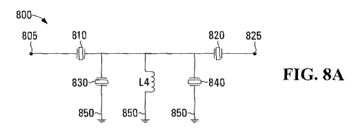
FIG_ BA is a schematic circuit illustration of
another embodiment of a self-matched band reject filter. In FIG.
8A, BRF 800 is considered to have an input port 805 and an
output port 825_ BRF 800 includes a single series resonator 810
and a single parallel resonator 830 on an input port side of
the BRF 800, which are coupled to a matching inductor L15. A
single parallel resonator 840 and a single series resonator 820
on an output port side of the BRF 800 are coupled to the
matching inductor L15. The two parallel resonators 830 and 840
and the matching inductor L15 are also coupled to ground 850.
FIG. BE is a representative illustration of an
implementation of BRF 800 of FIG, 8A as an acoustic resonator
interdigital transducer. Each resonator of the series
resonators and the parallel resonators of FIG. 8A includes a
plurality of consecutive interdigital transducer electrodes.
Series resonator 810 is formed by electrodes of transducer
element 803 and a first set of electrodes of transducer element
805. Series resonator 820 is formed by electrodes of transducer
element 826 and a first set of electrodes of transducer element
824. Parallel resonator 830 is formed by electrodes of
transducer element 807 and a second set of electrodes of
transducer element 805. Parallel resonator 840 is formed by
electrodes of transducer element 822 and a second set of
electrodes of transducer element 824. Element 860 of the
transducer is a short stub component that provides the desired
inductance for inductor L15. Element 850 of the transducer is a
ground bar.
CA 02743265 2011-05-10
WO 2010/048725 PCT/CA2009/001564
- 17 -
In some embodiments of the invention the thickness,
width and length of transducer element 860 are controlled
during fabrication of the BRF to control the value of the
inductance of inductor L15.
FIG. 9A is a schematic circuit illustration of
another embodiment of a self-matched band reject filter. FIG.
9A shows an example of cascading multiple BRFs. FIG. 9A
illustrates a BRF 900 that includes three BRFs 800A, 8008, 800C
cascaded together. These three BRFs substantially correspond to
the structure of BRF 800 of FIG. 8A. As described above, while
the structure of the elements of BRFS SODA, 8005, 8000 may be
substantially the same as that of BRF 800, the physical
parameters of the various elements is not necessarily the same.
FIG. 9B is a representative illustration of an
implementation of BRF 900 of FIG. 9A as an acoustic resonator
interdigital transducer. Three transducers 800A,800B,8000 of
the type illustrated in FIG. 8B are shown.
Although only three cascaded BRFs are shown in FIGs.
9A and 9B, the specific number of cascaded BRFs is
implementation specific. Furthermore, while three BRFs of the
same structure are cascaded together, it is to be understood
that when multiple BRFs are cascaded together to form a new BRF,
the multiple BRFs can be the same structure, with similar or
different parameters, or can be different structures.
FIG. 1OA is a schematic circuit illustration of a
further embodiment of a self-matched band reject filter- In FIG.
10A, a BRF 1000 includes a portion of the SRF 1000 that is
similar to the structure of BRF 800 of FIG. BA. The numbering
from FIG. 8A has been maintained in FIG. IOA for convention
purposes. Multiple series resonators 1010, only one being shown,
are coupled to an input side of the portion that is similar to
BRF 800. Multiple series resonators 1020, only one being shown,
CA 02743265 2011-05-10
WO 2010/048725 PCT/CA2009/001564
- 18 -
are coupled to the output side of the portion that is similar
to BRF 800.
FIG. 10B is a representative illustration of an
implementation of BRF 1000 of FIG. 10A as an acoustic resonator
interdigital transducer. A transducer similar to 800 of FIG. BE
is shown together with additional series resonator elements
1010 and 1020.
In some embodiments the use of connection bus bars
can be minimized resulting in a compact size of the BRF. For
example, this may include controlling any of the length, width
and thickness of transducer elements that for the BRF.
FIG_ 11A is a schematic circuit illustration of a
further embodiment of a self-matched band reject filter. In FIG.
11A, a BRF 1100 includes three cascaded portions 1000A, 10008,
1000C that are similar to BRF 1000 of FIG. 10A.
FIG. 11B is a representative illustration of an
implementation of BRF 1100 of FIG. 11A as an acoustic resonator
interdigital transducer. Three transducers 1000A, 10008, 1000C
of the type illustrated in FIG. 10B are shown.
In some embodiments the use of connection bus bars
can be minimized resulting in a compact size of the BRF. In
some embodiments such a cascaded design enables enhanced BRF
performance.
FIG. 12A is a schematic circuit illustration of a
further embodiment of a self-matched band reject filter. In FIG.
12A, BRF 1200 is considered to have an input port 1205 and an
output port 1275. BRF 1200 includes a first series resonator
1210 and a second series resonator 1220 of multiple series
resonators on an input port side of BRF 1200. A first parallel
resonator 1230 is coupled to the second series resonator 1220.
CA 02743265 2011-05-10
WO 2010/048725 PCT/CA2009/001564
- l9 -
A matching inductor L16 is coupled to the first parallel
resonator 1230. A second parallel resonator 1240 and a third
parallel resonator 1250 are coupled to the matching inductor
L16. Third series resonator 1260 and fourth series resonator
1270 of multiple series resonators on an output port side of
BRF 1200 are coupled to the third parallel resonator 1250. The
three parallel resonators 1230, 1240 and 1250 and the matching
inductor L16 are also coupled to ground 1280.
FIG. 12B is a representative illustration of an
implementation of BRF 1200 of FIG. 12A as an acoustic resonator
interdigital transducer. Elements for implementing the first,
second, third and fourth series resonators 1210, 1220, 1260 and
1270 and first, second and third parallel resonators 1230, 1240
and 1250 as well as matching inductor L16 are shown.
In some embodiments the use of connection bus bars
can be minimized resulting in a compact size of the BRF. For
example, this may include controlling any of the length, width
and thickness of transducer elements that for the BRF.
FIG. 13A is a schematic circuit illustration of a
further embodiment of a self-matched band reject filter. In FIG.
13A, BRF 1300 is considered to have an input port 1305 and an
output port 1385. BRF 1300 includes a first series resonator
1310 and a second series resonator 1320 of multiple series
resonators on an input port side of BRF 1300. A first parallel
resonator 1330 and a second parallel resonator 1340 are coupled
to the second series resonator 1320. A matching inductor L17 is
coupled to the second parallel resonator 1340. A third parallel
resonator 1350 and a fourth parallel resonator 1360 are coupled
to the matching inductor L17. Third series resonator 1370 and
fourth series resonator 1380 of multiple series resonators on
an output port side of BRF 1300 are coupled to the fourth
parallel resonator 1360. The four parallel resonators 1330,
CA 02743265 2011-05-10
WO 2010/048725 PCT/CA2009/001564
- 20 -
1340, 1350 and 1360 and the matching inductor L16 are also
coupled to ground 1390.
FIG. 13B is a representative illustration of an
implementation of BRA' 1300 of FIG. 13A as an acoustic resonator
interdigital transducer. Elements for implementing the first,
second, third and fourth series resonators 1310, 1320, 1370 and
1380 and first, second, third and fourth parallel resonators
1330, 1340, 1350 and 1360 as well as matching inductor L17 are
shown.
In some embodiments the use of connection bus bars
can be minimized resulting in a compact size of the BRF. For
example, this may include controlling any of the length, width
and thickness of transducer elements that for the BRF.
FIG. 14A.is a schematic circuit illustration of a
further embodiment of a self-matched band reject filter. In FIG.
14A, BRF 1400 is considered to have an input port 1405 and an
output port 1492. BRF 1400 includes a first series resonator
1410 and a second series resonator 1420 of multiple series
resonators on an input port side of PRF 1400. A first parallel
resonator 1430 and a second parallel resonator 1440 are coupled
to the second series resonator 1420. A matching inductor L18 is
coupled to the second parallel resonator 1440. A third parallel
resonator 1450, a fourth parallel resonator 1460 and a fifth
parallel resonator 1470 are coupled to the matching inductor
L18. Third series resonator 1480 and fourth series resonator
1490 of multiple series resonators on an output port side of
BRF 1400 are coupled to the fifth parallel resonator 1470. The
five parallel resonators 1430, 1440, 1450, 1460 and 1470 and
the matching inductor L18 are also coupled to ground 1495.
FIG. 14B is a representative illustration of an
implementation of BRF 1400 of FIG. 14A as an acoustic resonator
interdigital transducer- Elements for implementing the first,
CA 02743265 2011-05-10
WO 2010/048725 PCT/CA2009/001564
- 21 --
second, third and fourth series resonators 1410, 1420, 1480 and
1490 and first, second, third, fourth and fifth parallel
resonators 1430, 1440, 1450, 1460 and 1470 as well as matching
inductor L18 are shown.
In some embodiments the use of connection bus bars
can be minimized resulting in a compact size of the BRF. For
example, this may include controlling any of the length, width
and thickness of transducer elements that for the BRF.
FIG. 15A is a schematic circuit illustration of a
further embodiment of a self-matched band reject filter. In FIG.
15.A, BRF 1500 is considered to have an input port 1505 and an
output port 1592. BRF 1500 includes a first series resonator
1510 and a second series resonator 1515 of multiple series
resonators on an input port side of BRF 1500. A first parallel
resonator 1520, a second parallel resonator 1530 and a third
parallel resonator 1540 are coupled to the second series
resonator 1515. A matching inductor L19 is coupled to the third
parallel resonator 1540. A fourth parallel resonator 1550, a
fifth parallel resonator 1560 and a sixth parallel resonator
1570 are coupled to the matching inductor L19. Third series
resonator 1580 and fourth series resonator 1590 of multiple
series resonators on an output port side of BRF 1500 are
coupled to the sixth parallel resonator 1570. The six parallel
resonators 1520, 1530, 1540, 1550, 1560 and 1570 and the
matching inductor L19 are also coupled to ground 1595.
FIG. 15B is a representative illustration of an
implementation of BRF 1500 of FIG. 15A as an acoustic resonator
interdigital transducer. Elements for implementing the first,
second, third and fourth series resonators 1510, 1515, 1580 and
1590 and first, second, third, fourth, fifth and sixth parallel
resonators 1520, 1530, 1540, 1550, 1560 and 1570 as well as
matching inductor L19 are shown.
CA 02743265 2011-05-10
WO 2010/048725 PCT/CA2009/001564
- 22 -
In some embodiments the use of connection bus bars
can be minimized resulting in a compact site of the BRF. For
example, this may include controlling any of the length, width
and thickness of transducer elements that for the BRF.
By using SAW, FBAR and/or BAW design technologies,
some embodiments of the invention result in economically low
cost devices having a compact physical size.
Some aspects of the invention may find uses in
applications such as U-S. Patent Application No. 12/424,068
filed April 15, 2009, assigned to the assignee of the present
application.
According to a broad aspect of the invention, a radio
frequency band reject filter (BRF) includes an input port and
an output port. The radio frequency BRF includes a plurality of
acoustic resonators and an inductor for matching the impedance
of the plurality of acoustic resonators. The inductor is
positioned in the BRF in respect of the plurality of acoustic
resonators such that a static capacitance between the input
port and the inductor is substantially equivalent to a static
capacitance between the output port and the inductor.
In some embodiments, the four acoustic resonators are
one of: a plurality of parallel resonators; a plurality of
series resonators; and a combination of series and parallel
resonators.
In some embodiments, the combination of series and
parallel resonators comprise: N, where NZ2, series resonators;
and M, where MZ2, parallel resonators.
In some implementations when N is an even number,
there are N/2 series resonators between the input port and the
CA 02743265 2011-05-10
WO 2010/048725 PCT/CA2009/001564
- 23 -
inductor and N/2 series resonators between the output port and
the inductor.
In some embodiments, when M is an even number there
are M/2 parallel resonators between the input port and the
inductor and M/2 series resonators between the output port and
the inductor.
In some embodiments, each series and parallel
resonator that is part of a BRF is part of a transducer formed
by a set of interdigital electrodes extending from a pair of
parallel conductive elements.
In some embodiments, in the case of the parallel
resonators, at least one of the pair of parallel conductive
elements is coupled to ground.
In some embodiments, when at least one series
resonator or at least one parallel resonator, or both, are
coupled to at least one of the pair of parallel conductive
elements, the at least one conductive element is coupled to a
inductor.
In some embodiments the inductor is a short stub
element located between the at least one of the pair of
parallel conductive elements and ground.
In some embodiments the inductor is equal to or less
than 0.1 nH.
In some embodiments the BRF is one of multiple radio
frequency BRFs cascaded together with other radio frequency
BRFs.
In some embodiments, some or all of the other BRFs
each have a single inductor for matching the impedance of the
respective radio frequency BRFs.
CA 02743265 2011-05-10
WO 2010/048725 PCT/CA2009/001564
- 24 -
Referring to FIG. 16, a method for matching an
impedance in a radio frequency BRF will now be described. In a
first step 16-1, the method involves fabricating an input port
for the BRF. A second step 16--2 involves fabricating a
plurality of acoustic resonators. A third step 16-3 involves
fabricating an inductor for matching the impedance of the
plurality of acoustic resonators. A fourth step 16-4 involves
fabricating an output port.
The inductor is positioned in the band reject filter
in respect of the plurality of acoustic resonators such that a
static capacitance between the input port and the inductor is
substantially equivalent to a static capacitance between the
output port and the inductor.
In some embodiments, the plurality of acoustic
resonators is at least four acoustic resonators.
It is to be understood that the steps of the method
do not necessarily need to be performed in the specific order
described above. Depending on how the BRF is fabricated, for
example different materials are layered upon one another, the
input port, output port, acoustic resonators and the inductor
may be fabricated simultaneously, in the order described above,
or in a different order altogether.
Fabricating the BRF may be performed according to
known SAW, FBAR and BAW technologies, wherein fabricating the
inductor is controlled to provide a desired inductor.
With reference to FIG. 17, an example of a base
station 14 is illustrated. The base station 14 generally
includes a control system 20, a baseband processor 22, transmit
circuitry 24, receive circuitry 26, multiple antennas 28, and a
network interface 30. The receive circuitry 26 receives radio
frequency signals bearing information from one or more remote
transmitters provided by mobile terminals 16 (illustrated in
CA 02743265 2011-05-10
WO 2010/048725 PCT/CA2009/001564
- 25 -
FIG. 11) and relay stations 15 (illustrated in FIG. 12). A low
noise amplifier and a filter (not shown) may cooperate to
amplify and remove broadband interference from the signal for
processing. A BRF filter of the type described herein may be an
example of a filter included in the receive circuitry 26.
Dcwnconversion and digitization circuitry (not shown) will then
downconvert the filtered, received signal to an intermediate or
baseband frequency signal, which is then digitized into one or
more digital streams.
The baseband processor 22 processes the digitized
received signal to extract the information or data bits
conveyed in the received signal. This processing typically
comprises demodulation, decoding, and error correction
operations. As such, the baseband processor 22 is generally
implemented in one or more digital signal processors (DSPs) or
application-specific integrated circuits (ASICs). The received
information is then sent across a wireless network via the
network interface 30 or transmitted to another mobile terminal
16 serviced by the base station 14, either directly or with the
assistance of a relay 15.
On the transmit side, the baseband processor 22
receives digitized data, which may represent voice, data, or
control information, from the network interface 30 under the
control of control system 20, and encodes the data for
transmission. The encoded data is output to the transmit
circuitry 24, where it is modulated by one or more carrier
signals having a desired transmit frequency or frequencies. A
power amplifier (not shown) will amplify the modulated carrier
signals to a level appropriate for transmission, and deliver
the modulated carrier signals to the antennas 28 through a
matching network (not shown). Modulation and processing details
are described in greater detail below. A BRA' filter of the type
CA 02743265 2011-05-10
WO 2010/048725 PCT/CA2009/001564
- 26 -
described herein may also be included in the transmit circuitry
24.
With reference to FIG. 18, an example of a mobile
terminal 16 is illustrated. Similarly to the base station 14,
the mobile terminal 16 will include a control system 32, a
baseband processor 34, transmit circuitry 36, receive circuitry
38, multiple antennas 40, and user interface circuitry 42. The
receive circuitry 38 receives radio frequency signals bearing
information from one or more base stations 14 and relays 15. A
low noise amplifier and a filter (not shown) may cooperate to
amplify and remove broadband interference from the signal for
processing- A FRF filter of the type described herein may be an
example of a filter included in the receive circuitry 36.
Downconversion and digitization circuitry (not shown) will then
downconvert the filtered, received signal to an intermediate or
baseband frequency signal, which is then digitized into one or
more digital streams.
The baseband processor 34 processes the digitized
received signal to extract the information or data bits
conveyed in the received signal. This processing typically
comprises demodulation, decoding, and error correction
operations. The baseband processor 34 is generally implemented
in one or more digital signal processors (DSPs) and application
specific integrated circuits (ASICs).
For transmission, the baseband processor 34 receives
digitized data, which may represent voice, video, data, or
control information, from the control system 32, which it
encodes for transmission. The encoded data is output to the
transmit circuitry 36, where it is used by a modulator to
modulate one or more carrier signals that is at a desired
transmit frequency or frequencies. A power amplifier (not
shown) will amplify the modulated carrier signals to a level
appropriate for transmission, and deliver the modulated carrier
CA 02743265 2011-05-10
WO 2010/048725 PCT/CA2009/001564
- 27 -
signal to the antennas 40 through a matching network (not
shown). A BRF filter of the type described herein may also be
included in the transmit circuitry 24. Various modulation and
processing techniques available to those skilled in the art are
used for signal transmission between the mobile terminal and
the base station, either directly or via the relay station.
The above-described embodiments of the present
application are intended to be examples only. Those of skill in
the art may effect alterations, modifications and variations to
the particular embodiments without departing from the scope of
the application.
Numerous modifications and variations of the present
invention are possible in light of the above teachings. It is
therefore to be understood that within the scope of the
appended claims, the invention may be practised otherwise than
as specifically described herein.