Note: Descriptions are shown in the official language in which they were submitted.
CA 02743346 2011-06-16
1
TITLE OF THE INVENTION
Combined pn junction and bulk photovoltaic device
FIELD OF THE INVENTION
[0001] The present invention relates to solar cells and, in particular, to
improving the
efficiency of a solar cell by using various properties of multiferroic
materials.
BACKGROUND OF THE INVENTION
[0002] Pn or Schottky semiconductor junctions are at the basis of solar cells.
Basically, when
photons more energetic than the bandgap of the light absorbing semiconductor
are absorbed by a junction,
charge carriers, i.e. electrons and holes, are generated and separated by the
internal electric field developed
in the interfacial depletion zone. The limited charge transport through the p-
n junction and the presence of
energy barriers at the interfaces are factors affecting the power conversion
efficiency of the current solar
cells, i.e. the short-circuit photo-current density Jph and the open-circuit
photovoltage-Voc).
[0003] Recently, power conversion efficiency of 25% has been reported for
single-crystal
silicon solar cells.' Unfortunately such performance is still related to a
number of disadvantages, including for
example high material costs, high energy payback times, lack of physical
flexibility and additional
complicated processing steps such as providing passivation layer, anti-
reflection layer (AR)," grooves, buried
contact (BC) and back surface field (BSF), etc.. This is the case of the
double sided buried contact silicon
solar cells (DSBC) that were developed to solve the problem of hole-electron
recombination from rear
aluminum-alloyed region observed, due to the thermal process at high
temperature and for long times, in
single sides buried contact (SSBC). The SSBC cells or buried contact silicon
cells have been very
successful in overcoming most fundamental limitations associated with the
conventional screen-printed
metallization scheme. W In DSBC cells, however, a shunt path is needed between
the back surface electrode
and a floating junction layer to obtain the desired BSF effect. To solve this
problem, a self-biased solar cell
structure is introduced to reduce the hole-electron recombination at the rear
surface area, 1v However, this
method involves additional processing steps for connecting the front electrode
to the back electrode.
Furthermore, since BSF is obtained by using voltage generated by the solar
cell, its dimensions are limited
to values smaller than the open-circuit voltage (Voc).
CA 02743346 2011-06-16
2
[0004] Other structures based on ferroelectric films have been introduced to
increase the
efficiency of a single semiconductor solar cell.
[0005] Kim et al.v have suggested a method to achieve high efficiency in
single
semiconductor solar cells by using a ferroelectric material, by forming
ferroelectric layers on the front and the
rear surfaces of the semiconductor solar cell. The electric charge generated
by the spontaneous polarization
of these ferroelectric layers provides a surface passivation effect or a back
surface field, depending on the
position of the layers. Furthermore, with the deposited ferroelectric layers,
the open-circuit voltage of the
solar cell can be increased significantly while enhancing the energy
efficiency of the single semiconductor
solar cell.
[0006] Pulvarivi has proposed an efficient method based on a ferroelectric
material for
converting solar energy into electricity, by sandwiching, in the solar cell, a
very thin film of ferroelectric
insulator between a semiconductor and a metal electrode, thus forming a Metal-
Insulator-Semiconductor
(MIS) structure. In this case, the thermally induced electric charge produces
an inversion layer used to make
the desired pn junction.
[0007] In all techniques, however, loss by interfacial recombination of holes
and electrons is
increased due to the formation of a heterojunction at the semiconductor-
ferroelectric material interface.
Furthermore, the electrons mobility is limited due to the insulating effect
and large band gap of the
ferroelectric materials, which in turns results in lowering the efficiency of
the cell.
[0008] The photovoltaic effect observed in ferroelectric perovskite thin films
has recently
attracted attention due to its potential applications in the area of
optoelectronic devices and optical
information storage. In contrast to the conventional junction-based
interfacial photovoltaic effect in
semiconductors (i.e. p-n or Schottky junctions), the photovoltaic effect in
ferroelectrics is essentially a bulk
effect: the photo-generated charge carriers of both polarities are driven by
the polarization-induced internal
electric field in opposite directions towards the cathode and the anode,
respectively, and contribute to the
photovoltaic output. Increased photovoltaic power conversion efficiency for
ferroelectric thin films (around
0.28%) has been recently achieved with devices based on epitaxial La-doped
lead zirconate titanate (PZT)
films , although the efficiency of this material remains limited by its large
band gap. The availability of lower
band gap multiferroic oxides such as BiFe03 (BFO) and Bi2FeCrO6 (BFCO)E, F
provides alternative materials
to achieve a higher photovoltaic efficiency.
CA 02743346 2011-06-16
3
[0009] There is still a need in the art for high efficient solar cells
involving simplified
components structure and using simplified processing steps.
SUMMARY OF THE INVENTION
[0010] More specifically, there is provided an heterostructure comprising a
semiconductor
solar cell of a first band gap; a buffer layer formed on a front surface of
the semiconductor solar cell; and at
least one layer of a multiferroic or a ferroelectric material formed on the
buffer layer; wherein the at least one
layer of a multiferroic or a ferroelectric material has a second bang gap, the
first band gap being smaller than
said second band gap.
[0011] There is further provided a solar cell comprising a semiconductor solar
cell of a first
band gap; a buffer layer formed on a surface of the semiconductor solar cell;
and at least one layer of a
multiferroic or a ferroelectric material formed on the buffer layer; wherein
the at least one layer of a
multiferroic or a ferroelectric material has a second bang gap, the first band
gap being smaller than the
second band gap.
[0012] There is further provided a method for manufacturing a solar sell,
comprising
providing a semiconductor solar cell of a first band gap; forming a buffer
layer on a surface of the
semiconductor solar cell; and forming at least one layer of a multiferroic or
a ferroelectric material on the
buffer layer; wherein the at least one layer of a multiferroic or a
ferroelectric material has a second bang gap,
the first band gap being smaller than the second band gap.
[0013] Other objects, advantages and features of the present invention will
become more
apparent upon reading of the following non-restrictive description of specific
embodiments thereof, given by
way of example only with reference to the accompanying drawings
BRIEF DESCRIPTION OF THE DRAWINGS
[0014] In the appended drawings:
[0015] Figures 1 show the photovoltaic responses for Tin-doped indium oxide
(ITO)/BFCO/Nb-doped SrTiO3(001) heterostructure: (a) J-V characteristics
measured with incident light of
635nm (red), 410 nm (blue) and white light (mercury lamp); (b) power
conversion efficiency as a function of
CA 02743346 2011-06-16
4
red light Intensity; Insert of (b) Open-circuit voltage, Voc as a function of
light intensity; and
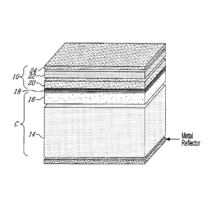
[0016] Figure 2 is a schematical view of an heterostructure according to an
embodiment of
an aspect of the present invention.
DESCRIPTION OF EMBODIMENTS OF THE INVENTION
[0017] In a nutshell, there is provided a method and a system to increase the
efficiency of
commercially available semiconductor solar cells by using simplified
structural components as well as
simplified processing steps.
[0018] There is described a method and a system allowing enhancing the
photovoltaic
efficiency of single semiconductor solar cells by making use of various
properties of functional and
multiferroic or ferroelectric materials.
[0019] According to an embodiment of an aspect of the present invention,
multiferroic
materials with good carrier transport properties and good visible light
absorption extending into the red range
are added to the base solar cell, providing a conductive, electron transparent
buffer layer of a perovskite
structure. They are selected with a small optical gap, i.e. in a range below
about 3 eV. The resulting
structure of the cells has good solar cells properties, including passivation
and anti-reflecting layer and back
surface field, and shows significant overall energy conversion efficiency.
[0020] Ferroelectric materials could also be used, added to the base solar
cell on top of a
conductive, electron transparent buffer layer of a perovskite structure. They
are selected with a band gap
below 3 eV and a crystal structure based on perovskite one and crystal cell
parameters allowing epitaxial
growth, such as, fo4r example Bi4Ti3O12, Bi6Ti4O17 and KTao.5Nbo.503
[0021] The present method and system provide a high efficiency solar cell
involving at least
one multiferroic or ferroelectric material layer, of a band gap larger than
the band gap of the base solar cell.
In the case of more than one multiferroic or ferroelectric material layer,
each upper layer is selected with an
increasing band gap.
CA 02743346 2011-06-16
[0022] For example, a new multiferroic material known as Bi2FeCrO6 (BFCO) may
be used
as the first layer of the multiferroic heterostructure. It has been discovered
that BFCO has surprising
photovoltaic properties and a small optical band gap. Figure 1 a shows the
current density versus voltage (J-
V) curves for a 120 nm-thick epitaxial BFCO film measured in the dark and
under different irradiations: red
light with X = 635 nm, blue with 2. = 410 nm and white (mercury lamp). The
measurements show a diode-like
behavior characterized by a directional leakage at positive voltage. In all
cases, photovoltaic effect was
observed in J-V curves taken under these illuminations. The open circuit
photovoltage Voc and the short
circuit photocurrent Jph were 0.63V and 0.13 mA.cm-2, 0.71V and 0.03 mA.cm-2,
0.55V and 0.009 mA.cm-2
under red, blue and white illumination respectively. The maximum external
power conversion efficiency was
calculated to be q about 8 % at a fill factor of about 0.68. These surprising
properties are thus used to
improve the energy efficiency of a conventional semiconductor solar cell. Jpn
is observed to increase almost
linearly with the illumination intensity (Figure 1 b), while Voc saturates at
high illumination intensity (Insert of
Figure 1 b).
[0023] Ordered BFCO thin films can be obtained artificially by depositing
alternatively BiFeO3
and BiCrO3 materials on (111) oriented single perovskite substrates.
[0024] A number of multiferroic materials could be used, including materials
based on the
ferroelectric-magnetic double perovskite structure, such as Bi2FeNiO6,
Bi2FeTiO6, Bi2FeMnO6, Bi2NiReO6,
Bi2MnReO6 and Bi2CoMnO6 for example.
[0025] Thus, multiferroic layers may be carefully superimposed on a base solar
cell, to
improve the separation process and transportation of the photogenerated
carriers through the resulting cell,
since the multiferroic materials exhibit a good bulk-photovoltaic effect which
additionally contributes to the
photocurrent and the photovoltage of the resulting cell.
[0026] In an example illustrated in Figure 2, the base solar cell (C) has a pn
structure with a
semiconductor substrate of a first conductive type (p or n) 14, a
semiconductor layer 16 of a second
conductive type (n or p) formed on the first conductive substrate 14, and a pn
junction formed at the
interface between the first conductive type semiconductor substrate 14 and the
second conductive type
semiconductor layer 16. The first 14 and the second 16 conductive type have
opposite polarities.
CA 02743346 2011-06-16
6
[0027] A buffer layer 18 is formed on the front surface of the second
conductive type
semiconductor layer 16. The buffer layer 18 is a doped film, such as N-doped
SrTiO3 or Nb-doped SrTiO3, of
a thickness selected so as to allow the tunneling mechanism. Since this
tunneling effect changes from
coherent below 1.5 nm to incoherent (variable range hopping) for thicker
films, the thickness of the buffer
layer 18 is selected between about 2 and about 5 nm. For the buffer layer 18
to allow creating the epitaxy
between the base solar cell and the heterostructure 10, it is selected so that
a maximum lattice mismatch in
relation to the material of the base solar cell and to the material of the
first layer deposited upon the buffer
layer is of about 7%. The buffer layer 18 will be discussed in more details
herein below, in relation to the
transportation of electrons between the bottom solar cell surface and the
first deposited multiferroic layer.
[0028] The heterostructure 10 comprises a small bandgap (for example between
1.3-2.0 eV)
multiferroic layer 20 formed on the buffer layer 18. The small bandgap
multiferroic layer 20 is shown here as
a thin film of Bi2FeCrO6 grown by pulsed laser deposition on the buffer layer
18, shown here as a (100)-
oriented Nb-doped SrTiO3.
[0029] In this example, the heterostructure 10 further comprises a larger
bandgap (for
example higher than 2.5 eV) multiferroic layer 22, such as for example
Bi2Fe2O6 or BiFeO3, superimposed
on the small bandgap multiferroic layer 20.
[0030] A transparent electrode 24 is formed on at least a part of the larger
bandgap
multiferroic layer 22. The transparent electrode 24 placed at the top of the
multiferroic heterostructure 10
comprises a transparent conductive oxide material (TCO), such as ITO (Indium
tin oxide), RU02, SrRuO3,
IrO2 or La1_xSrxCoO3 for example.
[0031] High crystal quality of the multiferroic heterostructure and layers
could be also grown
by methods usually applicable for other complex perovskite oxides, such as
metal organic chemical vapor
deposition (MOCVD), vapor-phase epitaxy (VPE), a modification of chemical
vapor deposition, Plasma-
enhanced chemical vapor deposition (PECVD), molecular beam liquid-phase
epitaxy (MBE and LPE),
Atomic layer deposition (ALD) and sputtering for example.
[0032] The operational effect of the multiferroic heterostructure 10
positioned at the front
surface of a solar cell will now be explained in detail in relation to Figure
2. The upper larger bandgap
multiferroic layer 22 absorbs higher-energy photons, and provides a
correspondingly large open-circuit
CA 02743346 2011-06-16
7
voltage; the low bang gap multiferroic layer 20 beneath absorbs lower-energy
photons and provides additive
contribution to the open-circuit voltage. Finally, all the photons not
absorbed by the preceding layers are
received by the conventional base solar cell (C), made of silicon for example,
which has the smallest
bandgap, for example 1.1 eV for the indirect bandgap of silicon.
[0033] The multiferroic materials used in the heterostructure 10 grown on the
solar cell (C)
are selected to have a similar crystal structure, i.e. a low mismatch lattice
constant (for example less than
3%), so as to yield optical transparency and maximum current conductivity
between the top and bottom
layers. The lattice mismatch limits the maximum thickness of the layer prior
to the onset of misfit
dislocations. 7% may be considered an upper limit, as it will limit the
thickness and the number of possible
techniques for deposition.
[0034] As a large mismatch in the crystal lattice may produce crystallographic
defects such
as misfit dislocations and potentially constitute a source for electron-hole
recombinations, multiferroic
materials with different bandgaps and closer lattice constants are selected,
such as, for example, BiFeO3 (a=
3.96Amg.) Bi2FeCrO6 (a=3.94 Amg.) and, the buffer layer may be SrTiO3 (a= 3.90
Amg). This tunnel oxide
junction is used as a buffer layer to promote epitaxial growth and high
crystal quality of the deposited
multiferroic heterostructure,vii. The epitaxial strain avoids the nucleation
of crystal defects which constitute
traps for holes and electrons; thus epitaxial strain improves the charge
transport through the layers
[0035] In particular, epitaxial growth of the multiferroic heterostructure
allows forming a self
polarized layer having a majority of the ferroelectric domains oriented in a
same direction, i.e. a
unidirectional spontaneous polarization, perpendicular to the solar cell
surface. As a result, deposition of a
polarized electrode and use of part of the cell's generated photovoltage for
polarizing the multiferroic
materials are not necessary, in contrast to known solar cells using
ferroelectric material.
[0036] As in the multi-junction solar cellsviil, the thickness of each
respective multiferroic layer
is carefully selected. As the layers are stacked in series, it is important
they each provide a same amount of
current. The current produced by a layer is directly proportional to the
number of absorbed photons. Since
the materials used for each layer have different photon absorption constants,
these differences are
compensated by different thicknesses. This means a material with a low
absorption constant will be used for
a thicker layer in the solar cell, so that each layer produces the same amount
of current.
CA 02743346 2011-06-16
8
[0037] Interestingly, the epitaxial strain, which results from lattice
mismatch, between the
buffer layer, such as SrTi03 for example, and the BFCO layer for example, can
be used to modulate the
optical gap of the BFCO material. Indeed, the strain directly affects the
structural parameters of BFCO (e.g.
the bond distances, angles and Fe/Cr cation ordering) and causes a
modification of the high hybridizing
energy effect between Fe, Cr and 0 on the density of states distribution in
the BFCO film. The strain gradient
usually present in epitaxial perovskite thin films can be advantageously used
here to design a desired gap
gradient in the same layer.
[0038] As people in the art will appreciate, the present system and method
provide a number
of advantages. As well known in the art, in traditional single semiconductor
solar cells most of the incident
solar energy is not converted into electricity, since when an incident photon
has less energy than the band
gap, it is not absorbed and passes through, and when an incident photon has
more energy than the band
gap, it is absorbed with the excess energy becoming heat, since the electron
can only absorb the band gap
energy. A multiferroic film or a ferroelectric grown on the front surface of
the solar cell according to the
present invention allows absorbing the high photon energy, thereby minimizing
this thermal effect and
allowing a more efficient photo-generation process.
[0039] Solar cells using multiferroic or ferroelectric materials as taught by
the present
invention have an improved photogenerated carrier separation process, in
particular for those carriers
generated in the solar cell. In addition to this self contribution to
photovoltaic properties of the overall solar
cell, a multiferroic or a ferroelectric layer formed on the top of the
conventional cell generates an internal
electric field at the near surface of the semiconductor, through the tunnel
junction, by way of its spontaneous
polarization. Therefore, electron-hole pairs are separated from each other and
their recombination is
prevented, and a surface passivation effect is obtained due to the formation
of a front surface field.
[0040] A multiferroic or a ferroelectric layer as used according to the
present invention may
further play the role of controlling the reflection of sunlight, depending
upon variation of the thickness thereof.
For example, a thin multiferroic layer on the top of the cell can play the
role of an anti-reflection layer and
reduce the light reflection at the front of the cell., while a thicker
multiferroic film deposited onto the rear of
the solar cell may act as a rear surface reflection (Back Surface Reflection)
for reflecting the light not
absorbed in the semiconductor back into the cell. In addition to enhancing the
energy efficiency of the solar
cell, the deposition of an additional anti-reflection layer (AR) or an Al-
based layer (forming the rear surface
filed) may thus be omitted, which simplifies the process steps currently used
for producing solar cells such
as Double Side Buried Contact Silicon Solar cells-DSBC for example.
CA 02743346 2011-06-16
9
[0041] The observed photovoltaic effect in the BFCO films could be useful as
the current
source for micro-electro-mechanical systems (MEMS). Optical sensors are
promising applications in the field
of MEMS. Until now, only semiconductors have been used but they have the
disadvantage of requiring the
application of bias voltage at the semiconductor p-n junction interface. In
the case of BFCO thin films the
zero-biais photocurrent is larger and thus is useful and applicable to MEMS.
[0042] Although the present invention has been described hereinabove by way of
embodiments thereof, it may be modified, without departing from the nature and
teachings of the subject
invention as defined in the appended claims.