Note: Descriptions are shown in the official language in which they were submitted.
CA 02744247 2013-11-20
ELECTROCHROMIC OPTICAL ELEMENT
HAVING AN APODIZED APERTURE
Field of the Invention
[0001] The present invention relates to an optical element comprised of an
electrochromic apodized aperture having variable light transmittance in
response to the magnitude of an applied electrical voltage.
Background of the Invention
[0002] The makers of mobile communication devices such as cellular
telephones continue to increase functionality of these devices. For example,
at present cellular telephones can include still and video cameras, video
streaming and/or two-way video calling capabilities. Users can capture still
or video images and transmit the image or video files via a network. While
the trend to increase functionality continues, manufacturers also continue to
reduce the size of such communication devices.
[0003] The reduced size of such mobile communication devices have
restricted the use of diaphragms with adjustable apertures or irises in the
cameras contained therein. A mechanical camera iris is a diaphragm having
a variable opening for a camera lens to alter the amount of light being
admitted as well as to adjust the depth of field available for the image. Such
mechanical irises are utilized in most film cameras and in many digital
cameras. A mechanical iris is not practical for use in mobile communication
devices because it would add too much bulk, increased costs, and may
have unreliable performance. Thus, manufacturers typically do not include
adjustable irises in cellular telephones. The consequence is that cellular
telephones neither produce good quality images at low light levels (due to,
for example, objectionable shot noise and readout noise) nor at high light
levels due, for example, to the inability to adequately decrease integration
times thereby creating over-saturation problems. Cellular
telephone
cameras also can exhibit poor depth of field and reduced image sharpness
due to lens aberration.
1
CA 02744247 2013-11-20
Summary of the Invention
[0004] The present invention is directed to an optical element comprising
an electrochromic apodized aperture having variable light transmittance in
response to the magnitude of applied electrical voltage. The apodized
aperture comprises (i) a first substrate having an outer surface and a planar
inner surface, (ii) a second substrate having an outer surface and a non-
planar inner surface opposing the planar inner surface of the first substrate,
and (iii) an electrochromic medium disposed between the planar inner
surface of the first substrate and the non-planar surface of the second
substrate. Each of the planar inner surface of the first substrate and the
non-planar inner surface of the second substrate has an at least partial layer
of conductive material thereover.
[0005] Also, the present invention is directed to an optical element
comprising an electrochromic apodized aperture having variable light
transmittance in response to the magnitude of an applied electrical voltage.
The apodized aperture comprises (i) a first substrate having an outer
surface and a planar inner surface, and (ii) a second substrate having an
outer surface and a convex inner surface opposing and spaced from the
planar inner surface of the first substrate to form a cavity therebetween.
Each of the planar inner surface and the convex inner surface has an at
least partial layer of transparent conductive material thereover; and (iii) an
electrochromic medium disposed within the cavity.
Brief Description Of The Several Views Of The Drawing(s)
[0006] Various non-limiting embodiments disclosed herein will be better
understood when read in conjunction with the drawings, in which:
FIG. 1 is a profile of an initial image of the aperture of the Example at
time 0 determined as described herein;
FIG. 2 is a profile of an image of the aperture of the Example after
about 1 second of applied voltage;
FIG. 3 is a profile of an image of the aperture of the Example after
about 4 seconds of applied voltage;
2
CA 02744247 2013-11-20
FIG. 4 is a profile of an image of the aperture of the Example after
about 18 seconds of applied voltage;
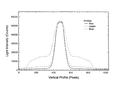
FIG. 5 is a profile of an image of the aperture of the Example after
about 110 seconds of applied voltage;
FIG. 6 is a profile of an image with_Gaussian curve fitting applied to the
Green line shown in FIG. 5;
FIG. 7 is a profile of the image resulting when no aperture was present;
FIG. 8 is a profile of the image resulting when the fixed aperture of the
Comparative Example was present;
FIG. 9 is a profile of an image with Gaussian curve fitting applied to the
Green line shown in FIG. 8; and
FIGS. 10A-D are schematic cross section views of the optical element
according to the present invention.
Detailed Description of the Invention
[0007] As used in this specification and the appended claims, the articles
"a", "an", and "the" include plural references unless expressly and
unequivocally limited to one referent.
[0008] Additionally, for the purposes of this specification, unless otherwise
indicated, all numbers expressing quantities of ingredients, reaction
conditions, and other properties or parameters used in the specification are
to be understood as being modified in all instances by the term "about."
Accordingly, unless otherwise indicated, it should be understood that the
numerical parameters set forth in the following specification and attached
claims are approximations. At the very least, and not as an attempt to limit
the application of the doctrine of equivalents to the scope of the claims,
numerical parameters should be read in light of the number of reported
significant digits and the application of ordinary rounding techniques.
[0009] All numerical ranges herein include all numerical values and ranges
of all numerical values within the recited ranges. Further,
while the
numerical ranges and parameters setting forth the broad scope of the
invention are approximations as discussed herein, the numerical values set
forth in the Examples section are reported as precisely as possible. It
3
CA 02744247 2013-11-20
should be understood, however, that such numerical values inherently
contain certain errors resulting from the measurement equipment and/or
measuring technique.
[0010] The present disclosure describes several different features and
aspects of the invention with reference to various exemplary
embodiments. It is understood, however, that the invention embraces
numerous alternative embodiments, which may be accomplished by
combining any of the different features, aspects, and embodiments
described herein in any combination that one of ordinary skill in the art
would find useful.
[0011] As previously mentioned, the present invention provides an optical
element 100, as referenced in Figures 10A-D, comprising an electrochromic
apodized aperture having variable light transmittance in response to the
magnitude of an applied electrical voltage. The apodized aperture 100
comprises:
(i) a first substrate 102, as referenced in Figures 10A-D, having an
outer surface and a planar inner surface,
(ii) a second substrate 102 having an outer surface and a non-planar
inner surface 106, as referenced in Figures 10A-D, opposing and spaced
from the planar inner surface of the first substrate 102, and
(iii) an electrochromic medium 110, as referenced in Figures 10A-D,
disposed between the planar inner surface of the first substrate 102 and the
non-planar surface 106 of the second substrate 102. Each of the planar
inner surface of the first substrate 102 and the non-planar inner surface 106
of the second substrate has an at least partial layer of conductive material
104 thereover. The respective refractive indices of the second substrate
102, and the electrochromic medium 110 can be substantially the same.
Also, the refractive index of the first substrate 102 (i) is substantially the
same as the respective refractive indices of the second substrate 102 (ii)
and the electrochromic medium 110 (iii). In the optical element 100 of the
present invention, a center region of the apodized aperture 100 defines a
"pupilary region" wherein the amount of the electrochromic medium 110 is
significantly less than that present in the remainder of the apodized aperture
4
CA 02744247 2013-11-20
100. This serves to minimize (or eliminate altogether) coloration in this
pupilary region. It has been found that the electrochromic aperture 1000f
the present invention offers several advantages over those previously
known, and, in particular, those where both of the opposing substrates 102
are convex, or both of the opposing substrates 102 are concave. The
electrochromic apodized aperture 100 of the present invention offers less
complexity in design (e.g., alignment of the two inner surfaces of the
opposing substrates 102 is not as critical) and thus less complexity in the
manufacture of the apodized aperture 100.
[0012] The first substrate 102 (i) and the second substrate 102 (ii) can be
comprised of the same or different materials. For example, the first and
second substrates 102 can comprise glass, such as fused silica or fused
quartz, or polymeric substrate materials. The first substrate 102 (i) can
comprise glass, and the second substrate 102 can comprise a polymeric
substrate material or vice versa. Likewise, the first substrate 102 (i) can
comprise glass, and the second substrate 102 (ii) can comprise glass.
Alternatively, the first substrate 102 (i) can comprise polymeric substrate
material, and the second substrate 102 (ii) can comprise polymeric substrate
material.
[0013] Suitable glass substrates 102 can include but are not limited to any
of those widely known (e.g., fused silica and fused quartz as previously
mentioned) and can include those having a refractive index of 1.40 or
greater, or 1.45 or greater, such as 1.50 or greater, or 1.65 or greater. In a
particular embodiment of the present invention, the substrate 102 (i) and/or
the substrate 102 (ii) can comprise a glass having a refractive index of 1.40
to 1.75.
[0014] Suitable polymeric substrates 102 can include without limitation
polycarbonate, polystyrene, polyurethane, polyurethane(urea), polyester,
polyacrylate, polymethacrylate, poly(cyclic) olefin, polyepoxy, copolymers
thereof, or mixtures of any of the foregoing. The polymeric substrates 102
can comprise a combination of any of the foregoing substrates 102, for
example, in the form of a multilayer laminate. The polymeric substrates 102
can be formed by any manufacturing means known in the art such as by
CA 02744247 2013-11-20
casting or molding, e.g., injection molding, techniques. In a
particular
embodiment of the present invention the polymeric substrate comprises
polycarbonates, poly(cyclic) olefins, polystyrenes, polyurethanes,
polymethacrylates, co-polymers of any of the foregoing materials, or
mixtures of any of the foregoing. Typically, both of the substrates 102 (i)
and (ii) are transparent (i.e., optically clear), however for some
applications
one or both may be tinted or otherwise colored. As used herein, by
"transparent" is meant a substrate that has a luminous transmittance of at
least 70 percent, such as at least 80 percent, or at least 85 percent.
Suitable polymeric substrates 102 can include without limitation those
having a refractive index ranging from 1.30 to 1.75, such as from 1.35 to
1.70.
[0015] As previously mentioned, the first substrate 102 (i) has an outer
surface and a planar inner surface, and the second substrate 102 (ii) has an
outer surface and a non-planar inner surface 106 opposing the planar inner
surface of the first substrate 102. The non-planar inner surface 106 of the
second substrate 102 (ii) typically is convex but may have a different
non-planar surface topography where desired, for example a spherical,
parabolic, or hyperbolic topography. In a particular embodiment, the second
substrate 102 (ii) (which has a non-planar inner surface) can comprise a
planar substrate having a partial-sphere or a half-sphere of the same or
different material affixed to the inner surface, thus forming a convex inner
surface, as shown in Figure 10A. Such a
partial-sphere or a half-sphere
configuration can be formed, for example, by dispensing a UV-curable
acrylic or epoxy resin material onto a planar surface of a glass or polymeric
substrate. This configuration provides flexibility for refractive index
matching
of the substrates 102 and the electrochromic medium 110 disposed
therebetween as discussed below.
[0016] Alternatively, the second substrate 102 (ii) can be a unitary piece
as shown in Figures 10B-D having a convex inner surface 106 comprised of
any of the aforementioned substrate materials. In any event, the curvature
of the convex inner surface 106 of the second substrate 102 (ii) is selected
such that maximum apodization of the aperture 100 is achieved.
6
CA 02744247 2013-11-20
[0017] At least one of the outer surface of the first substrate 102 (i) and
the
outer surface of the second substrate 102 (ii) can be substantially planar,
that is, at least one of the respective outer surfaces can be essentially free
of any wavefront distortion.
[0018] As aforementioned, each of the planar inner surfaces of the first
substrate 102 (i) and the non-planar inner surface 106 of the substrate 102
(ii) has an at least partial layer of transparent conductive material 104, as
referenced in Figures 10A-D, thereover. The conductive material 104 can
be selected from any of those widely known in the field of electrochromic
devices. For purposes of the present invention, the conductive material 104
typically comprises a transparent conductive material selected from carbon
nanotubes, gold, tin oxide, fluorine-doped tin oxide, indium tin oxide, and/or
one or more conductive polymers. Non-
limiting examples of suitable
conductive polymers can include poly(acetylene), poly(pyrrole),
poly(thiophene), poly(aniline), poly(fluorene), poly(pyridene), poly(indole),
poly(carbazole), poly(azine),
poly(quinone), poly(3-alkylthiophene),
polytetrathiafulvalene, polynaphthalene, poly(p-phenylene sulfide), and/or
poly(para-phenylene vinylene). For a
detailed discussion of suitable
conductive polymers, see Handbook of Conducting Polymers, 2nd ed., rev'd.,
Marcel Dekker, Inc., New York 1998. In the optical element 100 of the
present invention, the at least partial layer of transparent conductive
material
104 on the respective inner surfaces of the first substrate 102 (i) and the
second substrate 102 (ii) provides a surface conductivity ranging from 1 to
1000 ohm(s)/square, for example from 1 to 500 ohm(s)/square, such as
from 1 to 100 ohm(s)/square, or 3 to 80 ohms/square, or from 5 to 50
ohms/square.
[0019] In a particular embodiment of the present invention, the at least
partial layer of transparent conductive material 104 on the non-planar inner
surface 106 of the second substrate 102 (ii) opposes and is spaced from the
at least partial layer of transparent conductive material 104 on the planar
inner surface of the first substrate 102 (i). The spacing
distance
therebetween is dependent upon a number of factors, including but not
limited to the concentration of the electrochromic medium 110 and the
7
CA 02744247 2013-11-20
topography of the inner surface 106 of the second substrate 102 (ii). Taking
into account such factors, the spacing distance is selected such that the
coloration of the electrochromic medium 110 within the pupilary region of the
apodized aperture 100 is minimized or eliminated altogether. The
transparent conductive material 104 on at least one of the inner surface of
the first substrate 102 (i) and the inner surface 106 of the second substrate
102 (ii) can be electrically isolated in the pupilary region as shown in
Figures
10C-D. By the term "electrically isolated" in the pupilary region is meant
that
the transparent conductive material 104 within the pupilary region on the
inner surface of the first substrate 102 (i) is isolated or insulated (e.g.,
as
described below) from electrical communication with the transparent
conductive material 104 of the second substrate 102 (ii) or vice versa. This
permits direct contact between (i.e., no spacing between the respective
inner surfaces) the respective inner surfaces of the substrates 102 (i) and
(ii)
without effecting a short circuit.
[0020] It is contemplated that one or both of the respective inner surfaces
of the first substrate 102 (i) and the second substrate 102 (ii) can be
essentially free of the transparent conductive material 104 in the pupilary
region 114, as referenced in Figure 10D, of the apodized aperture 100.
This configuration provides an apodized aperture 100 wherein there is no
spacing between the first and second substrates 102 within the pupilary
region 114 (without creating a short circuit) and thus there is no coloration
in
the pupilary region 114. The apodized aperture 100 which is essentially free
of transparent conductive material 104 in the pupilary region 114 can be
achieved by simply masking the pupilary region 114 of one or both of the
respective inner surfaces of substrates 102 (i) and/or (ii), then applying the
transparent conductive material 104 to the inner surface(s), and
subsequently removing the mask to provide a pupilary region 114 free of
transparent conductive material 104 as shown in Figure 10D.
[0021] Alternatively, the transparent conductive material 104 in the pupilary
region 114 of one or both of the respective inner surfaces can be at least
partially removed, for example, by laser ablation techniques. In one
embodiment, the transparent conductive material 104 on a central portion of
8
CA 02744247 2013-11-20
the pupilary region of the inner surface of the first substrate 102 (i) and/or
the inner surface of the second substrate 102 (ii) can be isolated from the
remaining portion of the transparent conductive material 104 on that inner
surface by removing a fine line of the conductive material 104 around the
central portion using laser ablation techniques (i.e., creating an "island" of
conductive material 104 separated from the remaining conductive material
104 layer on that inner surface). This
permits direct contact of the
respective inner surfaces of the two substrates 102 (i.e., no spacing
between the two) without creating a short circuit.
[0022] Likewise, the transparent conductive material 104 on a central
portion of the pupilary region of the inner surface of the first substrate 102
(i)
and/or the inner surface 106 of the second substrate 102 (ii) can be
insulated from the remaining portion of the transparent conductive material
104 on that inner surface by applying a non-conductive organic or inorganic
coating material 112, as referenced in Figure 10C, (including any of those
known in the art) onto the central portion of the pupilary region (i.e.,
creating
an "island" of non-conductive material 112 over the conductive material 104
on that inner surface). This permits direct contact of the respective inner
surfaces of the two substrates 102 (i.e., no spacing between the two)
without creating a short circuit.
[0023] In a particular embodiment of the present invention, the non-planar
inner surface 106 of the second substrate 102 (ii) is essentially free of the
transparent conductive material 104 in the pupilary region. In this
alternative
embodiment, the pupilary region of the inner surface 106 of the second
substrate 102 (ii) which is essentially free of the transparent conductive
material 104 can be in direct contact with the transparent conductive
material 104 on the planar inner surface of the first substrate 102 (i),
provided that the conductive material 104 which is present on the inner
surface 106 of the second substrate 102 (ii) outside the pupilary region does
not contact the conductive material 104 on the inner surface of the first
substrate 102(i).
[0024] An electrochromic medium 110 (iii) is disposed between the
conductive layer 104 on the planar inner surface 106 of the first substrate
9
CA 02744247 2013-11-20
102 (i) and the conductive layer 104 on the non-planar inner surface 106 of
the second substrate102 (ii). The electrochromic medium 110 (iii) can
comprise any of the electrochromic materials known in the art, and can be
in any known form (for example, in the form of a liquid, a gel, or a polymeric
material). For example, the electrochromic medium 110 (iii) can be in the
form of solvent-phase electrochromic medium. For purposes of the present
invention, the terms "solvent-phase electrochromic medium" or
"solution-phase electrochromic medium" are intended to include
electrochromic media in the form of a liquid as well as a gel. In a particular
embodiment of the present invention, the electrochromic medium 10
comprises a solvent-phase electrochromic medium in the form of a liquid.
The electrochromic medium 110 includes at least one electrochromic
compound or dye, which varies in color or darkness in response to an
applied voltage. Typically, the electrochromic medium 110 used in the
optical element of the present invention includes electroactive cathodic and
anodic materials. In solution-
phase electrochromic media, the
electrochromic compound(s)/dye(s) are contained in a solution in an
ionically conducting electrolyte. The material remains in solution when
electrochemically reduced or oxidized.
[0025] Generally, the solvent-phase electrochromic medium 110 contains
at least one anodic electroactive dye, at least one cathodic electroactive
dye, and a small amount of salt(s) that is/are soluble in a suitable solvent.
When a DC voltage is applied across the two respective transparent
conductive layers 104 (typically separated by a low K material, e.g. a gasket
or seal member), the anodic dyes are electrochemically oxidized at the
surface of the anode and the cathodic dyes are electrochemically reduced at
the surface of cathode. Color formation is accomplished when the molar
extinction coefficient of the anodic dye and/or cathodic dye in the
solvent-phase electrochromic medium 110, change with their
electrochemical reactions. Generally, at least one of the dyes undergoes a
significant increase in extinction coefficient at a wavelength in the visible
range. These colored species are free to diffuse from the electrodes 104
(i.e., the respective transparent conductive layers) and meet each other in
CA 02744247 2013-11-20
the bulk of the electrochromic medium 110. A redox reaction takes place
between the two electrochemically changed dyes to regenerate their
respective original states (i.e., the bleached or non-colored states). The
final coloration of the apodized aperture 100 is the result of an equilibrium
between the electrochemical reaction at the electrode surfaces 104 (i.e., the
respective surfaces of the transparent conductive layers) and a diffusion
controlled redox reaction in the bulk of the solvent-phase electrochromic
medium 110. In such a
"self erasing cell", a current at a given applied
voltage is required to maintain the apodized aperture 100 in the colored
state. Without the
applied voltage, the cell will eventually return to its
original bleached state.
[0026] Notwithstanding the foregoing, the electrochromic coloration within
the electrochromic apodized aperture 100 can be enhanced by applying a
progression of voltage pulses. The pulses can be applied either by pulsing
voltage on and off, or by pulsing between two different applied voltages,
and/or by pulsing to reverse polarity in order to reverse current flow
direction. Coloration and de-coloration can be affected by adjusting (either
individually or in any combination) the amplitude of applied voltage pulses
(in either the positive or negative direction), the pulse time, and/or pulse
frequency.
[0027] Also, it is contemplated that the apodized aperture 100 can be
structured to accommodate the resistive heating of the apodized aperture
100, for example, through the use of a quick burst of battery power through
one or both of the transparent conductive layers 104 in plane (and not
across the electrochromic medium 110). Heating the aperture 100 not only
serves to increase the kinetics of coloration of the electrochromic medium
110, but also to increase the rate of fading back to the bleached state ("fade
rate").
[0028] The electrochromic medium 110 employed in the optical element
100 of the present invention can comprise any of the electrochromic
compounds known in the art, including, for example, phenazine compounds,
such as dihydro-phenazine compounds, and/or dipyridinium (i.e., viologen)
compounds. Suitable non-limiting examples of such phenazine compounds
11
CA 02744247 2013-11-20
and the preparation thereof can include those described in U.S. 6,020,987 at
column 31, line 43, column 34, line 7, and in U.S. 4,902,108 at column 13,
line 49 to column 15, line 42. Suitable
non-limiting examples of viologen
compounds include those described in U.S. 6,020,987 at column 34, line 8-
55. See also, Electrochromism and Electrochromic Devices, Monk et al.,
Cambridge University Press 2007, Chapter 11, pp.341-373. Specific
examples of suitable anodic electrochromic dyes can include but are not
limited to 5,10-dihydro-5,10-dimethylphenazene, N,N,N,N"-tetramethy1-1,4-
phenylenediamine, 10-methylphenothiazine, 10-
ethylphenothiazine,
tetrathiafulvalene, ferrocene and derivatives thereof, and/or triarylamines
and derivatives thereof. Specific
examples of suitable cathodic
electrochromic dyes can include but are not limited to 1,1 '-dipheny1-4,4"-
bipyridinium difluoroborate, 1, 1"-di(n-hepty1)-4,4"bipyridinium
difluoroborate,
1, 1"-dibenzy1-4,4" bipyridinium defluoroborate, and/or 1,1"-di(n-
propylpheny1)-4,4"-bipyridinium difluoroborate.
[0029] In addition, the electrochromic medium 110 also may include other
materials such as solvents (e.g., polar aprotic solvents), light absorbers,
light
stabilizers, thermal stabilizers, antioxidants, thickeners or viscosity
modifiers
(e.g., polyvinylpyrrolidone), and free standing gel, including polymer
matrices. The electrochromic medium 110 can include a solvent comprising
propylene carbonate, benzonitrile, phenoxyacetonitrile, diphenyl acetonitrile,
sulfolane, sulfolate, and/or phosphoramide Other
useful solvents can
include, but are not limited to phosphoric esters such as tricresyl phosphate,
cresyl phosphate and the like, amides such as N,N-di-methylformamide,
methylpropionamide, N-methylpyrrolidone, hexamethylphosphonamide,
diethylformamide, tetramethylurea and the like, nitriles such as acetonitrile,
sulfoxides such as dimethylsulfoxide, esters such as ethyl acetate, butyl
acetate, dioctyl phthalate and the like, carbonates such as propylene
carbonate, ethylene carbonate and the like, lactones such as .gamma.-
butyrolactone, ketones such as methyl ethyl ketone, methyl isobutyl ketone
and the like. Any of the aforementioned solvents maybe used singly or in
any combination. The viscosity of the solvent can influence the response
12
CA 02744247 2013-11-20
speed of the electrochromic coloration. Thus, when higher response speeds
are needed, solvents of lower viscosity typically are used.
[0030] Additionally, the solution-phase electrochromic medium 110 can
comprise a dissolved electrolyte, for example, tetrabutylammonium
tetrafluoroborate and/or tetrabutylammonium bromide to provide ionic
conductivity to the solution. Electrolyte materials suitable for this purpose
are well known in the art.
[0031] As previously mentioned, in the optical element 100 of the present
invention, the refractive indices of the second substrate 102 (ii), and the
electrochromic medium 110 (iii) can be substantially the same. By
"substantially the same" refractive index is meant that the difference
between the respective refractive indices of each of the second substrate
102 (ii), and the electrochromic medium 110 (iii) is not more than +/- 0.005,
for example not more than +/- 0.004, or not more than +/- 0.003, or not
more than +/- 0.002. Thus, the second substrate 102(ii) and the
composition of the electrochromic medium 110 (iii) are selected such that
the respective refractive indices of (ii) and (iii) are substantially the
same.
Also, the respective refractive indices of the first substrate 102 (i), the
second substrate 102 (ii), and the electrochromic medium 110 (iii) can be
substantially the same. Such a "match" of refractive indices of 102 (ii) and
110 (iii), and where desired 102 (i), provides an optical element 100 having
excellent optical qualities.
[0032] It should be noted that if the differences between the respective
refractive indices of the substrate 102 (ii) and the electrochromic medium
110 (Hi), and, where desired, the first substrate 102 (i), are greater than
those values stated above, for example, a difference of about +/- 0.01, or a
difference of about +/- 0.1, the optics of the optical device in which the
apodized aperture 100 is employed, (e.g., a cellular telephone camera)
could be modified to adjust for this lack of refractive index matching. Simply
put, in some instances it may not be desirable to "match" the refractive
indices of102 (ii) and 110 (iii), and where desired 102 (i), as discussed
above. In such instances, the optical power of the optical element 100 can
be maintained by adjusting the various components of the optical element
13
CA 02744247 2013-11-20
100 itself, and/or by adjusting one or more of the components of the device
in which the optical element 100 is employed. For example, when the
apodized aperture 100 is used in a cellular telephone camera, the apodized
aperture 100 can be used in conjunction with a camera lens having a
particular power. Likewise, power can be introduced in one or both of the
substrates 102 of the apodized aperture 100 itself. The apodized aperture
100 itself may be used as a lens by balancing the respective shapes and
refractive indices of the first and second substrates 102, as well as by
adjusting the electrochromic medium 110.
[0033] In the optical element 100of the present invention, the
electrochromic apodized aperture 100 can further comprise at least one seal
member 108, as referenced in Figures 10A-D, (iv) about the outer perimeter
of the apodized aperture 100 and in contact with the first substrate 102 (i),
the second substrate 102 (ii), and the electrochromic medium 110 (iii) to
protect and contain the electrochromic medium 110 between the transparent
conductive layers 104 on the respective inner surfaces of the first and
second substrates 102. Such a seal member 108 should be comprised of a
material having good adhesion to glass and/or polymeric substrate 102
materials, and to the conductive layers 104. Also, the seal member 108
should exhibit low permeabilities for oxygen, moisture vapor and other
gases, and should not interact with or contaminate the electrochromic
medium 110 it is meant to contact and contain. Suitable materials for use as
the seal member 108 include, but are not limited to thermoplastic,
thermosetting and UV curing organic sealing resins such as any of those
known for use in liquid crystal devices. (See U.S. Patent Nos. 4,297,401,
4,418,102, 4,695,490, 5,596,023, and 5,596,024.) Suitable materials for use
as the perimeter seal member 108 are low K materials as mentioned above.
Several non-limiting examples of suitable seal materials can include those
based on epoxy, polyolefin (such as polypropylene, polyethylene,
copolymers and mixtures thereof), silicones, polyesters, polyamides and/or
polyurethane resins. Any of the aforementioned materials can be silane-
modified to enhance the bonding thereof to the substrate materials, e.g.
14
CA 02744247 2013-11-20
glass. Suitable adhesives can be used where appropriate to adhere the
seal member 108 to the substrates 102 (i) and (ii).
[0034] Also, it should be noted that of one or more adhesives such as any
of those known in the art, can constitute the seal member 108. Suitable
adhesives for the purpose can include but are not limited to adhesives
based on thermoplastic, thermosetting and UV curing organic resins.
Suitable adhesives can include, for example, those based on epoxy,
polyolefin (such as polypropylene, polyethylene, copolymers and mixtures
thereof), silicones, polyesters, polyamides and/or polyurethane resins. The
use of solder glass materials
is contemplated as well.
[0035] Obviously, any physical contact between the respective transparent
conductive layers 104provided on the inner surface of the substrate 102 (i)
and on the inner surface 106 of the substrate 102 (ii) (which serve as
electrodes) should be avoided in order to prevent shorting (i.e., a short
circuit) during operation of the apodized aperture 100. Thus, in particular
embodiments of the present invention, the respective transparent conductive
layers 104 should be spaced one from the other. The aforementioned seal
member 108 itself can serve as a spacer, and/or separate optical element
members comprised of insulating materials can be used as spacers to
maintain the physical separation of the respective transparent conductive
layers 104.
[0036] As used herein, the term "apodized" and related terms (e.g.,
apodizing, apodization, etc.) refer to an aperture 100, which has a smooth
and gradual transition along its radius from the greatest percentage of
transmitted light (e.g., at the center of the aperture 100) to the lowest
percentage of transmitted light (e.g., at the edges of the aperture 100). A
fully apodized aperture 100 would be one for which light transmittance (T)
varies along its radius (x) as a Gaussian curve (that is, T=exp(ax2). When
employed as an optical element, for example, as a camera iris, the
electrochromic apodized aperture 100 of the present invention emulates the
pupil of the human eye in that it facilitates automatic "dilation" and
"constriction". As the excitation energy increases, the aperture 100
CA 02744247 2013-11-20
constricts so as to reduce the amount of light through the lens. The
constricting aperture 100 enabled by the present invention changes (i.e,
increases) the effective f-number of the lens system and therefore increases
its depth of field. Similarly, as the excitation energy decreases, the
aperture
100 dilates so as to increase the amount of light through the lens. As the
aperture 100 becomes completely transparent the full aperture 100 is limited
only by the lens mechanical stop (assuming no other system elements serve
as limiting factors). Thus, the apodized aperture 100 is characterized by a
Gaussian radial transmittance curve. The thickness of the electrochromic
medium 110 increases along a radius of the apodized aperture 100 and
varies with the non-planar (e.g., convex) inner surface 106 of the second
substrate 102.
[0037] Generally, the at least partial layers of transparent conductive
material 104 on the inner surface of the first substrate 102 (i) and the inner
surface 106 of the second substrate 102 (ii) serve as counter-conducting
electrodes in electrical communication with a controller which is operable to
energize the electrochromic aperture 110 by applying an electrical voltage
thereto. The magnitude of the electrical voltage applied varies in response
to light conditions as determined, for example, by a photo sensor, such as
the CMOS image sensor of a typical cell phone camera module. As
previously mentioned, the present invention provides an apodized aperture
100 which "opens" to allow a greater amount of light to pass through in low
lighting conditions (i.e., where the electrochromic medium 110 is
de-energized by reducing or removing application of voltage); and which
"closes" to attenuate or block a portion of light when conditions are brighter
(i.e., where the electrochromic medium 110 is energized by application of an
applied voltage). The electrochromic medium 110 thus provides an
apodized aperture 100 having a smooth and gradual transition along its
radius from the greatest percentage of transmitted light (e.g., at the center
of
the aperture 100 in the pupilary region) to the lowest percentage of
transmitted light (e.g., at the edges of the aperture 100) in order to provide
improved resolution and overall focusing, for example by a lens and sensor.
The electrochromic medium 110 may be automatically energized and/or de-
16
CA 02744247 2013-11-20
energized and/or continuously varied in response to changes in the sensed
lighting conditions surrounding the imaging array sensor, thereby providing
improved illumination of the sensor during low light conditions while further
providing improved focusing and greater control of lens aberrations during
higher light conditions.
[0038] In a particular embodiment, the present invention is directed to an
optical element comprising an electrochromic apodized aperture 100 having
variable light transmittance in response to the magnitude of an applied
electrical voltage, the apodized aperture 100 comprising: (i) a first
substrate 102 having an outer surface and a planar inner surface, and (ii) a
second substrate 102 having an outer surface and a convex inner surface
106 opposing and spaced from the planar inner surface of the first substrate
102 to form a cavity therebetween, wherein each of the planar inner surface
and the convex inner surface 106 has an at least partial layer of transparent
conductive material 104 thereover, the conductive material 104 comprising,
for example, indium tin oxide; and (iii) an electrochromic medium 110
disposed within the cavity. The refractive indices of the second substrate
102, and the electrochromic medium 110 can differ by not more than +/-
0.003. In this embodiment, the electrochromic apodized aperture 100
further can comprise a seal member 108 (iv) comprised of any of the
aforementioned seal member materials about the outer perimeter of the
apodized aperture 100 and in contact with the first substrate 102 (i), the
second substrate102 (ii), and the electrochromic medium 110 (iii). A
suitable adhesive can be used to affix the seal member to the substrates
102 (i) and (ii), or the adhesive itself can serve as the seal member 108.
The refractive indices of 102 (i), 102 (ii) and 110 (iii) can differ by not
more
than +/- 0.003. Further, at least one of the outer surface of 102 (i) and the
outer surface of (ii) is substantially planar.
[0039] The electrochromic apodized aperture 100 of the present invention
usually is implemented in conjunction with a pixilated imaging array sensor,
such as a CCD or CMOS chip. However, the electrochromic apodized
aperture 100 can be implemented in conjunction with other types of sensors,
17
CA 02744247 2013-11-20
and may be implemented with or without a color filter or process associated
with the sensor, without affecting the scope of the present invention.
[0040] In any of the optical element(s) of the present invention the
respective outer surfaces of the first and second substrates 102 of the
apodized aperture 100 can be at least partially coated with at least one
coating chosen from protective coatings, such as hard coats and/or
abrasion-resistant coatings, anti-reflective ("AR") coatings, antifogging
coatings, oxygen barrier coatings and/or infra-red (IR) absorbing coatings
and/or IR reflective coatings, and/or conventional reflective coatings
connected to at least a portion of the outer surface of one or both of the
substrates 102. Note that the coatings can, but need not, cover an entire
outer surface. Suitable non-limiting examples of AR coatings can include a
monolayer coating or multi-layer coating of metal oxides, metal fluorides, or
other such materials, which may be deposited onto the outer surface(s) of
the substrates 102 (i) and/or (ii) or, alternatively onto self-supporting
films
that are applied to the substrate 102 outer surface(s), through application
means such as vacuum deposition and sputtering techniques as are well
known in the art. Suitable non-limiting examples of IR reflective coatings
can include very thin, partially transparent metallic layers such as NiCr
and/or or gold layers applied, for example, by PVD metallization methods.
Such materials and application means are available from Creavac
Vakuumbeschechtung GmbH of Dresden, Germany. Suitable examples of
IR reflective coatings (e.g., Laser Gold and Laser Black) also are available
from Epner Technology, Inc. Also, suitable IR reflective coatings can
include the silver-based coatings available under the tradename AgHTTm,
and the gold-based coating available under the tradename AuARETM, from
CPFilms Inc. of Canoga Park, CA. Suitable non-limiting examples of IR
absorbing coatings are coatings which comprise IR absorbing dye materials,
for example, those which are photochemically stable under ambient light
conditions, and which absorb light within the near-IR region of the spectrum,
for example, 5,5'-
dichloro-11-diphenylamino-3,3'-diethy1-10,12-
ethylenethiatricarbocyanine perchlorate (which provides peak IR absorption
at about 830 nm); 2,4 di-3-guaiazuleny1-1,3-dihydroxycyclobutenediylium
18
CA 02744247 2013-11-20
dihydroxide, bis(inner salt) (which provides peak IR absorption about 780 to
about 800 nm); and 1-butyl-24243[(1-butyl-6-chlorobenz[cd]indo1-2(1H)-
ylidiene)ethylidene]- 2-chloro-
5-methyl-1-cyclohexen-1-yl]ethenyI]-6-
chlorobenz[cd]indolium tetrafluoroborate (which provides peak IR blocking at
about 900 to about 1000 nm).
[0041] Transitional coatings may also be employed. As used herein the
term "transitional coating" means a coating that aids in creating a gradient
in
properties between two coatings. For example, although not limiting herein,
a transitional coating can aid in creating a gradient in hardness between a
relatively hard coating and a relatively soft coating. Examples of
transitional
coatings include radiation-cured acrylate-based thin films.
[0042] Suitable
examples of protective coatings can include, but are not
limited to, abrasion-resistant coatings comprising organo silanes, abrasion-
resistant coatings comprising radiation-cured acrylate-based thin films,
abrasion-resistant coatings based on inorganic materials such as silica,
titania and/or zirconia, organic abrasion-resistant coatings of the type that
are ultraviolet light curable, oxygen barrier-coating, UV-shielding coatings,
and combinations thereof. For
example, the protective coating can
comprise a first coating of a radiation-cured acrylate-based thin film and a
second coating comprising an organo-silane. Examples
of commercial
protective coatings products include SILVUE 124 and HI-GARD
coatings, available from SDC Coatings, Inc. and PPG Industries, Inc.,
respectively.
[0043] Various embodiments disclosed herein will now be illustrated in the
following examples.
Examples
Section I describes the preparation of the electrochromic solution 110
and index matching of the solution and lens. Section II describes the
fabrication of the electrochromic iris 100. Section III describes the methods
used to test the electrochromic iris 100 of the present invention and a fixed
aperture Comparative Example. Section IV describes the imaging results for
the Example and Comparative Example presented as Figures 1-9.
19
CA 02744247 2013-11-20
Section l ¨ Preparation of Electrochromic Solutions
Part A - Preparation of n-heptyl viologen tetrafluoroborate
Preparation of n-heptyl viologen tetrafluoroborate was carried out in
two steps. The
following materials were purchased from Aldrich without
purification: n-heptyl bromide, 99% (629-04-9), 4, 4'-bipyridine (553-26-4)
98%, acetonitrile (75-05-08), sodium tetrafluoroborate (13755-29-8) and
tetrabutylammonium tetrafluoroborate (429-42-5).
Step 1 - Preparation of Dibromides
To a 1,000 ml three necked round bottom flask was added acetonitrile
(200 mL), 4, 4'-dipyridine (0.08 mole, 12.5 g) and of n-heptyl bromide (0.25
mole, 45.23 g) and the solution was agitated by a mechanical stirrer. The
resulting clear yellow solution was heated to boiling over about a 30 minute
interval. After about 2 hours and 30 minutes, the solution turned darker and
yellow precipitates formed. The solution was refluxed at 80 C for about 16
hours and afterwards was cooled to room temperature. The yellow precipitate
was separated by filtration, washed with fresh acetonitrile and air dried
yielding 26.5 g of the product. The recovered product was used in Step 2
without further purification.
Step 2 - Salt Exchange/Purification
Sodium tetrafluoroborate (0.22 moles, 24.15 g) was dissolved in
approximately 700 mL of deionized water in a one liter beaker with mixing and
the product of Step 1 (0.045 mole, 23.1 g) was added. The yellow product of
Step 1 gradually changed color to white at ambient temperature. After 2
hours of mixing, the white precipitate was recovered by filtration using a
Buchner funnel with No. 54 filter paper to yield about 26 g of product. The
recovered product was dried under vacuum in an oven at 90 C for several
hours yielding 21.4 g of product. Analysis by an area % HPLC assay revealed
it to be 99.9%. The product (10 g) was recrystallized from 250 mL of
deionized water in a 600 mL beaker. The resulting suspension was heated
and became clear when the temperature was about 90 C. The hot clear
solution was filtered through No. 40 filter paper into two 300 mL Erlenmeyer
flasks that were heated on the same hot plate. The resulting filtrates were
CA 02744247 2013-11-20
allowed to cool to ambient temperature and a crystalline precipitate formed.
The recrystallized product (6.8 g) was analyzed by an area % HPLC assay
which indicated 100% without detectable impurities.
Part B - Preparation of Cell Solution
The following materials were obtained from Aldrich without purification:
propylene carbonate (108-32-7), benzonitrile (100-47-0), 5, 10-dihydro-5, 10-
dimethylphenazine (DMPZ, 15546-75-5), and polyvinylpyrrolidone (PVP,) with
typical Mw = 1, 3 MM (9003-39-8). TINUVIN P ultraviolet light absorber was
obtained from Ciba Geigy. Refractive index at 589 nm/20 C was measured
through a digital refractometer from ATAGO, Automatic Digital Refractometer
model RX-7000a following the manufacturer's recommended procedures in
the Instruction Manual Cat. No.3262.
Step 1 ¨ Preparation of Solvent Mixture
Benzonitrile (50.88 g) and propylene carbonate (49.12 g) were mixed
together in a suitable container. The refractive index of the resulting
mixture
was 1.4816.
Step 2 ¨ Preparation of a 3% PVP Solvent Mixture
Polyvinylpyrrolidone (3 g) was dissolved into the product of Step 1
(97.0 g). The refractive index of the resulting solution was 1.4819.
Step 3 ¨ Preparation of Stock Solution
Into a suitable container was added the product of Step 2 (20.0 g).
Tetrabutylammonium tetrafluoroborate (0.10 M, 0.6585 g) and TINUVIN P
ultraviolet light absorber( 0.0200 g) were added with mixing. The refractive
index of the resulting solution was 1.4821.
Step 4 ¨ Preparation of Electrochromic Cell Solution (0.06M)
n-Heptyl viologen tetrafluoroborate (0.1584 g) was dissolved into the
product of Step 3 ( 5.0 g) resulting in a clear colorless solution. To the
solution was added DMPZ (0.0631 g) and the color of the clear solution
became greenish. The refractive index of the resulting solution was 1.4844.
Part C ¨ Index Matching of the Electrochromic Cell Solution to the N-FK5
Hemispheric Lens
In order to match the refractive index of 1.4890 of N-FK5 glass 102
(Schott) used for the electrochromic iris 100 lens at a wavelength of 550 nm,
it
21
CA 02744247 2013-11-20
was determined that the cell solution 110 needed to match a refractive index
measured at 589 nm of 1.4851 0.0003, based on the optical dispersion
curve. The optical dispersion curve was determined using a Metricon Prism
Coupler, Model 2010M and was calculated using the Cauchy fit module of the
instrument operating software version 1.81.
The adjusting of the refractive index from 1.4844 to 1.4851 was carried
out by adding a 3 weight % PVP solution in 100% benzonitrile (0.0374 g) to
the product of Step 4 (2.7550 g). The resulting solution was stirred with
about
0.5 g of 4A molecular sieve beads (8-12 mesh) for about 16 hours and filtered
through a 0.45 micron cartridge. The resulting refractive index at 589 nm was
1.4850. Since the refractive index obtained was within 0.0003, no further
adjusting was needed.
Section II ¨ Fabrication of the Electrochromic Iris
The following materials were used: two Indium tin oxide 104 coated
glass slides 102 measuring 25 mm by 25 mm by 1.1 mm, item X-178 from
Delta Technologies; two 30 gauge needles; a hemispherical lens 106
prepared from a 2.5 mm ball lens of N-FK5 glass obtained from MSPT, Inc.
Mountain View, CA. that was ground down by Opticfab Corp. Santa Clara,
CA. until resulting in a hemispherical lens 106 having the curvature of the
2.5
mm ball lens and a thickness of about 300 microns; Loctite M-I2IHPTM
Hysol Medical Device Epoxy Adhesive; and DYMAX Light Weld 429-gel
glass adhesive;
Onto one of the ITO 104 coated glass slide 102 a rectangular space
measuring 20 by 25 mm was used to locate the components used to prepare
the cell. This space was defined by one edge where a 30 gauge needle was
positioned at one top corner and another 30 gauge needle was positioned at 5
mm from the edge of the other top corner. The hemispherical lens 106 was
placed in the center of the 20 by 25 mm rectangle. Another ITO 104 coated
glass slide 102 was placed over the rectangle so that a 5 mm edge from each
of the ITO 104 coated slides was exposed. The resulting assembly was held
together with miniature binder clips attached at the top and bottom of the
assembly. The epoxy adhesive 108 was used to fill the gap at two opposite
22
CA 02744247 2013-11-20
ends of the cell without touching the needles. The cell was allowed to cure at
ambient temperature overnight to fix the thickness of the cell and then the
needles were removed. More epoxy adhesive 108 was used to fill the cell gap
of all four sides except an approximately 0.2 mm inlet at one edge. The cell
was then cured at 105 C for one hour to complete the process. Afterwards
the cell was placed with the inlet down into a beaker containing the index
matched electrochromic cell solution 110 of Part C and placed into a vacuum
chamber for 5 minutes at about 30 inches of mercury. The vacuum was
slowly replaced with nitrogen gas to enable the cell solution to be drawn up
into the assembly 100. After the cell was vacuum filled with the product of
Part
C the opening was sealed with the DYMAX Light Weld 429-gel glass
adhesive and cured by exposure to ultraviolet light in a DYMAX 5000-EC
chamber for 7 seconds. The resulting cell was cleaned with acetone and both
of the exposed ITO 104 coated surfaces were covered with copper conductive
tape (about 6.3 mm wide) coated on the attached side with a conductive
adhesive to serve as a busbar for easy electric connection. The resulting cell
100 was exposed to ultraviolet light in the DYMAX 5000-EC chamber again
for 7 seconds. The busbars of the cell 100 were connected to a LAMBA Model
LLS5018 power supply. When the voltage was increased to greater to 0.6 V to
1.2 V the cell colored. When the voltage was decreased below 0.6 V the cell
100 began bleaching to the original colorless appearance.
Section III ¨ Methods used to test the Electrochromic Iris 100
The product 100 of Section II was placed in a mounting fixture about 40
to 60 mm
beneath the objective of an Olympus SZH1 0 zoom
stereomicroscope being illuminated from the diffuse light source with
maximum intensity. The microscope was set up using the 1.5x objective with
the zoom setting set for 2.5. The aperture on the microscope was set to value
6. The mounting fixture was connected to a stage containing a manual plastic
shutter.
In order to minimize the effects of room lighting, the eyepieces of the
microscope were covered with black plastic covers and black light blocking
material. Black plastic light blocking material was also wrapped around the
23
CA 02744247 2013-11-20
microscope stage area. The busbar areas of each side of the electrochromic
cell 100 were attached to a LAMBDA LLS5008 digital power supply set to
deliver 1.2 volts.
Images were acquired using an AVT Stingray 145C color digital
camera mounted onto the microscope using a C-Mount connector. The digital
camera was attached to a computer using a FireWire 800 cable and Firewire
PCI card. Images were acquired using AVTs software (SmartView 1.10). The
camera was set up using the following settings: Format = F7 Mode 0, ISO
speed = 400, Width = 1388, Length = 1038, Integration time = 140
milliseconds, high signal to noise ratio = 8 images, frames per second = 0.85,
and all auto-adjusting features, such as white balance, were turned off.
Images were acquired for 300 images at a rate of 0.85 frames per second. Of
the 300 images, approximately 24 images were acquired with the voltage to
the sample being off, about 100 images with the voltage on at 1.2 V, about
100 images with the voltage off and about 75 dark images (manual shutter
between the light source and the sample closed). The dark images were
averaged and used to subtract out the dark noise from the camera system in
the profiles shown below. The images were saved in RAW format.
The data was analyzed using Igor Pro (version 6.1x) from
WaveMetrics, customized to auto analyze all the images acquired during the
data acquisition. The images were loaded into Igor Pro and converted from
RAW format to RGB format using a debayering function of RGRG....
GBGB... as indicated in the AVT Stringray manual. Besides converting the
images from RAW to RGB, no additional image processing was performed on
the images analyzed and represented by Figures 1-9. The images for the "no
aperture" in Figure 7 and Comparative Example "fixed aperture" (300 micron
precision pinhole, mounted, from Edmund Optics, NT56-285) in Figures 8 and
9 were collected using the same set-up except the integration time was 120
milliseconds and the frames per second was 0.98. The intensity profile
extracted from each analyzed image was along a vertical line through the
center of the image.
In addition to analyzing the images as a function of time, the software
was programmed to display a cross-sectional "intensity" profile of the iris
100
24
CA 02744247 2013-11-20
as a function of time. Note that the profiles shown are from data with the
average dark image information subtracted out along the same coordinates as
the profile. The average dark image was an average of 60 to 75 frames with
the plastic shutter in the closed position (no light present). Also note that
the
profiles were extracted from vertical rows of the data and averaged over +/- 8
pixels to improve the signal to noise.
Section IV ¨ Imaging Results
The intensity profiles for the electrochromic iris 100 were derived from
images taken for Figure 1 at time 0, for Figure 2 at about 1 second, for
Figure
3 at about 4 seconds, for Figure 4 at about 18 seconds, and for Figure 5 at
about 110 seconds. Figure 6 shows the curve fitting of a Gaussian curve onto
the green response curve line of Figure 5 after 110 seconds. Figure 7
represents the profile with no aperture in place. Figure 8 represents the
Comparative Example of a fixed 300 micron aperture. The analyzed images of
the iris 100 were collected via the SmartView 1.10 software (with auto white
balance applied before data acquisition and then white balance was fixed)
and displayed in Igor Pro. The intensity profiles of the figures show the red,
green and blue (solid curve, large dashes and small dashes, respectively)
curves that were derived from the vertical rows of data on the images.
The profiles of Figures 1-6 demonstrate the function of an
electrochromic apodized iris 100. When the voltage is off, the iris 100 is
full
open in Figure 1. When 1.2 V are applied, the electrochromic iris 100
activates forming an apodized aperture as demonstrated after about 1 second
in Figure 2, after about 4 seconds in Figure 3, after about 18 seconds in
Figure 4 and after about 110 seconds in Figure 5. Figure 6 demonstrates how
closely the green response (dashed curve) of Figure 5 closely represents a
Gaussian distribution (solid curve), which is useful for apodization. The
Gaussian width parameter obtained using Igor Pro's built in Gaussian fit
routines (with the resulting width parameter equal to Sqrt(2)*standard error)
was converted to a more traditional beam waist calculation for Gaussian
beams [2* standard error] by dividing the Igor Pro width parameter by Sqrt(2)
and multiplying that result by 2. The Gaussian width (beam waist) of the
CA 02744247 2013-11-20
apodized aperture was about 316 microns. The Comparative Example "fixed
aperture" profile (width about 300 microns +/- 10 microns) is shown in Figure
8 and applied Gaussian curve fitting to the profile in Figure 9. The profile
in
Figure 9 clearly demonstrates the difference between an apodized aperture
100 (solid curve) and a fixed aperture (dashed curve). Figure 7 demonstrates
a profile with no aperture present.
Whereas particular embodiments of this invention have been described
above for purposes of illustration, it will be evident to those skilled in the
art
that numerous variations of the details of the present invention may be made
without departing from the invention as defined in the appended claims.
26