Note: Descriptions are shown in the official language in which they were submitted.
CA 02745589 2011-06-02
WO 2010/068417 PCT/US2009/065655
ADAPTIVE IMPEDANCE MATCHING (AIM)
FOR ELECTRICALLY SMALL RADIO RECEIVER ANTENNAS
FL _______________________ h __ LD OF THE INVENTION
[0001] This invention relates to antenna systems, and more particularly
to impedance
matching in antenna systems.
BACKGROUND OF THE INVENTION
[0002] The size and aesthetics of many AM/FM receivers constrain the
dimensions of
their antennas and their ground planes to suboptimal limits.
[0003] For simplicity and performance, the desired size of a good-
perfouning antenna
is about one-half wavelength at the tuned frequency (e.g., a halfwave dipole).
Although
longer antennas can offer better antenna gain, their narrow beamwidths make
them
impractical for most applications. At FM frequencies, a half wavelength is
about 1.5 meters,
while for AM frequencies it is about 150 meters. Due to the presence of
sensitivity-limiting
ambient noise, which is greater at lower frequencies, it turns out that 1.5
meters is a sufficient
length for both FM and AM receivers. A vertical quarter-wave whip antenna
mounted over a
large ground plane (e.g., a metal car body) exhibits perfounance similar to a
halfwave dipole
antenna, and affords good FM and AM reception in cars.
[0004] AM/FM receivers are available in many configurations, including
automotive,
tabletop, MP3 players, and cell phones. Smaller devices are typically
characterized by poor
signal reception, since halfwave and quarter-wave antennas are too large and
impractical. An
antenna size less than a half wavelength is considered electrically small.
Electromagnetic
interference (EMI) caused by antenna proximity to electronics, signal
variability due to
human body effects, and variable antenna orientation all have a significant
impact on antenna
performance. Because these effects are more pronounced at lower frequencies,
many small
devices have FM-only receivers.
[0005] The impedances of any antenna and receiver can theoretically be
matched to
achieve maximum power transfer. This can be realized by conjugate matching
antenna and
receiver impedances. Although it is well-known that conjugate matching of the
antenna and
receiver input impedances maximizes power transfer into the receiver, it is
not necessarily
optimum for receiver sensitivity. Conjugate impedance matching is practical
for half
wavelength antennas with relatively low reactance, and resistance nearly
constant across the
band, but this approach is not practical for the electrically small antennas
used in many devices.
The radiation and loss resistance of these antennas is very low, and the
reactance is high. This
- 1 -
CA 02745589 2011-06-02
WO 2010/068417 PCT/US2009/065655
high ratio of reactance to radiation resistance leads to matching techniques
that maximize the
voltage (not power) delivered to the receiver input.
[0006] The reactance of electrically small antennas can be tuned out using
a resonant
matching circuit. The Q of the resonant circuit thus formed must be held
sufficiently high to
increase the signal voltage to an acceptable level at the input to the
receiver low noise amplifier
(LNA). To achieve a sufficiently high Q, the receiver LNA must present a high
parallel
resistance to the antenna resonant circuit. Although higher values may be
possible and could
improve reception, a Q of about 30 is a practical goal for AM and FM
reception.
[0007] Since a high Q circuit has a narrow bandwidth, it must be tunable
across the AM
or FM band as the receiver is tuned. This was common practice for AM tabletop
superheterodyne receivers with internal loop antennas. The receiver mixed the
RF input signal
to a fixed intermediate frequency (IF) using a local oscillator (LO), mixer,
and IF filter. The
antenna for these receivers was either an air-loop (typical of older tube
receivers) or a smaller
ferrite-core loop antenna, both having similar characteristics. Since the
inductance of this
internal loop antenna was fixed and not significantly affected by external
factors (such as the
human body), a preselection filter was tuned along with the receiver LO to
maintain a high Q
resonant peak at the tuned frequency. This preselection filter, comprised of
the loop antenna's
inductance and a variable capacitance, also served as an image reject filter.
Older
superheterodyne receivers used a ganged-capacitor method to synchronize the
preselection filter
tuning with the LO tuning.
[0008] More modern receivers typically perform a similar function with
varactor diodes
acting as voltage-controlled capacitors. The voltage for the varactor diode of
the preselection
filter is derived from the tuning voltage of the LO varactor diode. Factory
calibration is usually
necessary for these receivers to accommodate component tolerances.
Unfortunately, it is
impractical for some modern receivers to utilize preselection filter tuning.
The receiver IF is
sometimes incompatible with this type of tuning, and calibration and
consistency over operating
temperature become impractical. Furthermore, external and portable antennas
have time-
varying impedance characteristics, making fixed factory calibration
impossible.
SUMMARY OF THE INVENTION
[0009] In a first aspect, the invention provides a method of tuning an
antenna circuit
including: (a) receiving a signal on an antenna, (b) producing a received
signal strength
indication based on the received signal, (c) using the received signal
strength indication to
produce a control voltage, (d) using the control voltage to control a
capacitance in an antenna
- 2 -
CA 02745589 2011-06-02
WO 2010/068417 PCT/US2009/065655
matching circuit, (e) changing the control voltage to minimize a ratio of a
change in the
received signal strength indication to a change in the control voltage, and
(f) repeating steps
(a), (b), (c), (d) and (e).
[0010] In another aspect, the invention provides an apparatus, including
an antenna, a
circuit for producing a received signal strength indication based on the
received signal, a
processor for using the received signal strength indication to produce a
control voltage, and an
antenna matching circuit including a capacitance controlled by the control
voltage, wherein the
processor changes the control voltage to maximize signal gain by minimizing a
ratio of a change
in the received signal strength indication to a change in the control voltage.
[0011] In another aspect, the invention provides an apparatus including
means for
receiving a signal on an antenna, means for producing a received signal
strength indication
based on the received signal, means for using the received signal strength
indication to
produce a control voltage, and means for using the control voltage to control
a capacitance in
an antenna matching circuit, wherein the means for using the received signal
strength
indication to produce a control voltage changes the control voltage to
maximize signal gain
by minimizing a ratio of a change in the received signal strength indication
to a change in the
control voltage.
BRIEF DESCRIPTION OF THE DRAWINGS
[0012] FIG. 1 is a schematic diagram of an antenna circuit filter.
[0013] FIG. 2 is a schematic diagram modeling resistor noise in an
antenna circuit
filter.
[0014] FIG. 3 is a graph of received signal strength versus frequency.
[0015] FIG. 4 is a block diagram of a radio receiver and an antenna.
[0016] FIG. 5 is a block diagram of a radio receiver and an antenna.
[0017] FIG. 6 is a schematic representation of an adaptive impedance
matching cycle.
[0018] FIG. 7 is a flow diagram of a method of producing a control
voltage.
[0019] FIG. 8 is a graph of control voltage, delta, and direction versus
adaptive
impedance matching cycles.
[0020] FIG. 9 is a graph of a filter gain and received signal strength
indication versus
adaptive impedance matching cycles.
[0021] FIG. 10 is a flow diagram of an adaptive impedance
matching/automatic gain
control update cycle.
- 3 -
= CA 02745589 2014-11-27
. =
79461-112
DETAILED DESCRIPTION OF THE INVENTION
100221 In one aspect, this invention provides an Adaptive Impedance
Matching (AIM)
technique. AIM is an adaptive feedback technique which attempts to maintain
maximum signal gain at the tuned frequency. In one example, resonant tuning of
a high Q
preselection filter is achieved using a signal metric from a baseband
processor. As the received
signal level decreases (due to listener tuning, antenna orientation, human
body effects, etc.), the
baseband processor adaptively retunes the preselection filter to provide
maximum signal voltage
to the low noise amplifier (LNA). AIM eliminates the need for receiver
calibration associated
with existing preselection filter tuning techniques, and is independent of the
intermediate
frequency (N), since local oscillator (LO) tracking is not performed.
[0023] For portable AM receivers, a small ferrite loopstick antenna is
often the best
choice. Although the sensitivity of an AM receiver with a small loopstick
antenna is
generally not very good, it is relatively easy to construct a varactor-tuned
circuit with high Q
to increase signal gain.
[0024] AM reception is especially challenging for a portable receiver.
FM broadcast
signals are generally transmitted with both vertical and horizontal
polarization, making the
receiver antenna orientation less critical than for AM, which has only
vertical polarization.
This makes positioning and orientation of the AM loopstick antenna more
crucial than for
FM. Furthermore, placement of a loopstick antenna within a receiver makes it
more
susceptible to EMI generated by the receiver electronics, especially at AM
frequencies.
[0025] Portable and hand-held analog FM radio receivers often use an
earbud wire
antenna, which may be Configured as either a short dipole or monopole.
Although one might
imagine an earbud wire as a dipole with one leg for each ear, this would yield
poor
= performance due to the limited distance between elements of the antenna
(much less than a
half wavelength).
[0026] Another short dipole configuration places the antenna feed and
receiver in a
= small accessory that clips to the listener's lapel. One leg of the dipole
would extend up
toward the ears, while the other would drape down to the waist where it would
connect to the
= main device (e.g., MP3 player). This dipole configuration is not common
and suffers from
poor performance because it is shorter than a half wavelength.
[0027] The more common monopole earbud wire antenna requires a ground
plane to
replace the lower element of a dipole. Ideally, the ground plane for an FM
monopole should
- 4 -
=
CA 02745589 2011-06-02
WO 2010/068417 PCT/US2009/065655
be at least one square meter, and a ground plane the size of a metal car body
is preferred.
However, hand-held portable devices are typically much smaller than a quarter
wavelength,
which seriously compromises performance. One way to effectively increase the
ground plane
size is to add a meander spiral to the receiver printed circuit board (PCB).
The inductive
reactance of the spiral cancels some of the highly capacitive reactance of the
small ground
plane, thereby improving signal coupling into the receiver. Although this
approach has some
utility at higher frequencies, it provides little sensitivity improvement at
FM (and especially
AM) frequencies.
[0028] Another portable FM antenna option is a small loop located within
the
receiver. This is an especially attractive choice for portable FM receivers
that do not use
earbud wires (e.g., a wireless Bluetooth headset). Location within the
receiver makes it
aesthetically pleasing and easy to use. Receiver size is not important because
loop antennas
do not require a ground plane. On the other hand, its small size makes a loop
a less-efficient
signal collector than an earbud wire, and its placement within the device
leaves it more
susceptible to EMI. It has been shown, however, that human body proximity to a
loop
actually improves reception sensitivity, whereas the sensitivity of earbud
wire antennas is
generally degraded. Furthermore, it has been demonstrated that a small loop
antenna can
achieve a higher Q than an earbud wire, partially offsetting its smaller size.
As a result, a
loop antenna could be an attractive diversity element in a receiver that also
includes an earbud
wire antenna.
[0029] As stated above, a practical technique for matching electrically
small antennas
is to maximize the signal voltage at the receiver low noise amplifier (LNA)
input. This can
be done by conjugate matching the antenna and receiver input reactances. The Q
of the
resulting parallel resonant circuit determines the voltage delivered to the
receiver LNA.
Resonant circuit Q is largely determined by the LNA parallel input resistance.
The higher the
input resistance, the higher the Q, and therefore the higher the signal
voltage. Of course,
resistor noise also increases with receiver input resistance, so the net
effect of Q on reception
sensitivity is not as pronounced.
[0030] Consider a small square loop antenna in free space connected to a
receiver
with a high-impedance input. This configuration can be modeled as the resonant
antenna
circuit filter shown in FIG. L Resistors Ra and &as represent the radiation
and loss
resistances of the loop antenna, and inductor La represents the loop
inductance. R is the
- 5 -
CA 02745589 2011-06-02
WO 2010/068417 PCT/US2009/065655
parallel input resistance of the LNA, and C is the sum of the LNA input
capacitance and any
additional capacitance needed to tune out the inductive reactance of the
antenna.
[0031] The transfer function of this antenna circuit filter is:
H a(f) = __________________________________________________________
R+ Ra +R10, ¨(2g = f)2 = R = La = C + j =2g = f =[R = C = (R, + La].
[0032] Evaluating at resonance, the magnitude of the antenna circuit
filter transfer
function is:
es)1= ________________________________________________________
r
R+ Ra +R10õ ¨(2g = f)2 = R = La = C + j .2g = f .[R = C =(Ra + Ria,c)+ La]
1
f 2ir=VLõ C
Ra '2' g = frõ .[R = c =(Ra+-Rh,) La].
[0033] Since the loop is small, its radiation and loss resistance can be
considered
negligible. In this case, FIG. 1 becomes a simple parallel resonant circuit
and the magnitude
of the antenna circuit filter transfer function at resonance reduces to:
______________________________________________ = Q (1)
j = 2 7r = fres = La XL
where Q is the quality factor of the parallel resonant circuit. This indicates
that the gain of
the small loop antenna circuit filter at resonance is equal to its Q.
[0034] All antennas have an effective height he which, when multiplied by
the electric
field strength E, yields the open circuit induced antenna voltage:
Vsjg(f)=E=he(f)=
[0035] The effective height of a loop antenna depends upon the frequency f
in Hz,
loop area A in square meters, permeability põ, and number of turns N:
he(f)= 277- = f N = A = ,uõ
where c = 3x10⁸ m/s is the speed of light. For air-loop antennas, pec = 1.
[0036] From FIG. 1, it is evident that the LNA input voltage
(f) =Vs,g(f)= Ha (f). Then the voltage at the LNA input at resonance is given
by:
- 6 -
CA 02745589 2011-06-02
WO 2010/068417
PCT/US2009/065655
27-r = fres =N = A=Q=E
(2)=
[0037] Reception sensitivity is a function of not only the gain of the
antenna circuit
filter, but also of the LNA, resistor, and ambient noise. For an electrically
small loop
antenna, the radiation resistance is very low, so the ambient noise can be
considered
negligible. Furthermore, one can assume that the resistor noise dominates the
LNA noise in a
well-designed receiver. The antenna circuit filter used to determine the
resistor noise
contribution in the small loop antenna configuration is shown in FIG. 2. The
resistor noise is
modeled as an ideal voltage source V,,01se,R in series with a noiseless
resistor R.
[0038] The transfer function of the resistor noise antenna circuit filter
is:
+ RThcs + j = 27z- = f = La
H N,R(f)=
R Ra
RIOSS (27-1- f)2 = R = Lõ = C + j = 27-1- = f =[R = (Rõ + Ri0õ). C + Lai
[0039] Again, assuming negligible radiation and loss resistance for the
small loop
antenna, and evaluating at resonance,
HN,R(Les) =
= 271" ' fres = La .
j = 27-t- = fres = L,
[0040] From FIG. 2, the resistor noise voltage density VAI,R at the LNA
input is the
product of the open circuit resistor noise voltage V.
aoise,R and the transfer function of the
resistor noise antenna circuit filter:
VN,R(f) =IF I N,R(f)I.Vnorse,R '
[0041] The open circuit noise voltage of a resistor R is given by the well-
known
relation:
Vnorse,R .\14 = k = To = R
where k 1.38x10⁻²³, J/K is Boltzmann's constant, and To = 290 degrees Kelvin
is room
temperature. For the small loop antenna, IHN,R0 I is unity at resonance, so
the resistor noise
voltage density at the LNA input is:
VN,R = V4=k=To=R. (3)
- 7 -
CA 02745589 2011-06-02
WO 2010/068417 PCT/US2009/065655
[0042] Reception sensitivity is defined as the electric field strength
needed to achieve
a desired signal-to-noise ratio at the receiver LNA input. Using equations (2)
and (3), the
signal-to-noise ratio at the LNA input for a small loop antenna is:
127-c=fe, =N=A=Q=E\2
v
SNR = _______________________
VN2,R 4 = k = To = R
[0043] Solving for reception sensitivity E:
c = -\14 = k = To = R = SNR
E=
27r=f,.õ=N=A=Q
[0044] For a parallel resonant circuit:
XL
Q= ____________________________________
[0045] Using this definition to substitute for R in the previous
expression for E yields:
(4)
4 k = To = SNR = La
E= __________________________
N = A \ 27r = f,.õ = Q
[0046] Equation (1) indicates that, for a small loop antenna at
resonance, the received
signal gain is equal to the Q of the antenna circuit filter. However, equation
(4) shows that
reception sensitivity improves only as the square-root of Q, due to effects of
resistor noise.
Thus, one would expect that for a received signal level increase at the LNA
input of N dB, the
net sensitivity increase would be only N/2 dB. Although illustrated for a
small loop antenna,
this relationship between signal gain and sensitivity applies in general to
all antenna types.
So the sensitivity of the receiver in dB includes a 10 = log(Q) term.
ADAPTIVE IMPEDANCE MATCHING
[0047] Although high Q antenna circuit filters can improve signal gain
and reception
sensitivity, they must be accurately tuned. The higher the Q, the more
demanding are the tuning
requirements. Antenna reactance can be variable and unpredictable, depending
on listener
movement and relative orientation of the antenna to the human body. As a
result, impedance
matching to the receiver is generally very lossy.
[0048] To overcome this problem, existing portable receivers often
include the
antenna in a docking station. This solution is undesirable, however, because
the antenna
element is not portable and cannot travel with the listener.
- 8 -
CA 02745589 2011-06-02
WO 2010/068417 PCT/US2009/065655
[0049] It is desirable to have an antenna design that overcomes these and
other
problems, particularly for use with a portable, hand-held receiver for
receiving analog and
digital radio broadcast signals.
[0050] Resonant tuning of a high Q circuit can be achieved by controlling
the voltage
applied to a varactor diode with variable capacitance depending upon this
voltage. As the
received signal quality degrades (due to listener tuning, antenna impedance
changes, human
body effects, etc.), the receiver adaptively retunes the circuit with the
tuning voltage to
provide maximum signal voltage to the LNA. This process, referred to as
Adaptive
Impedance Matching (AIM), is illustrated in FIG. 3, In FIG. 3, the resonant
peak occurs at
the receiver tuned frequency when the received signal strength indication
(RSSI) is at level
(1). As the RSSI changes, the resonant peak shifts as shown in FIG. 3.
[0051] The AIM seeks to maximize antenna gain at the receiver tuned
frequency. A
feedback control loop is used to accomplish this goal. A simplified, generic
functional block
diagram of a receiver 10, antenna 12, and antenna circuit filter 14 is shown
in FIG. 4.
Antenna circuit filter replaces the preselection tuning function of some
existing receivers. A
signal on line 16 from the antenna circuit filter is used to produce an
antenna tuning control
signal on line 18. The diagram shows that the antenna tuning control signal is
derived from
an AIM algorithm within the receiver, instead of tracking an LO voltage, as in
superheterodyne receivers using a preselection filter.
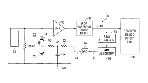
[0052] FIG. 5 is a functional block diagram of a receiver 20 with a loop
antenna 22
tuned by varactor diodes 24, 26 under AIM feedback control. A loop antenna is
used here as
a generic example, appropriate for either FM or AM applications. Electrically
small
antennas, typically having low radiation resistance and high reactance (e.g.,
a small internal
loop antenna), can often be tuned with a varactor-controlled tuning circuit
28. This circuit is
tuned to provide a resonance gain peak at, or very near, the center frequency
of the desired
input signal.
[0053] The tuned antenna circuit filter is comprised of the inductance L
of the loop
antenna and the capacitance C of the varactor diodes, along with any other
stray capacitance
or inductance, including human body effects. A damping resistor Rdamp, in
concert with the
LNA input resistance, is used to set the Q of the tuned circuit.
[0054] The receiver is shown to include a low noise amplifier 30 having a
high input
impedance, an IF or baseband signal filter 32 and other components commonly
found in
receivers such as a demodulator, detector, etc. as shown in block 34. Tuning
the antenna
- 9 -
CA 02745589 2011-06-02
WO 2010/068417 PCT/US2009/065655
circuit filter to a desired frequency is accomplished by applying a voltage to
a varactor diode
that provides the appropriate capacitance for the tuned frequency. This tuning
control voltage
is the feedback signal generated by the AIM algorithm, shown in block 36. The
AIM
algorithm receives a received signal strength indication (RSSI) estimation 38
from the filtered
IF or baseband signal on line 40. The AIM algorithm outputs a control value on
line 42,
which is converted to an analog control voltage on line 44 by a digital-to-
analog converter 46.
The analog control voltage is filtered by a filter 48, comprised of resistors
50, 52 and
capacitor 54 to produce a filtered control voltage at point 56. A back-to-back
varactor diode
pair, as shown in FIG. 5, is preferred over a single varactor, to improve
linearity.
[0055] Assuming negligible radiation and loss resistance, the simple loop
antenna
circuit shown in the example of FIG. 5 has a transfer function of:
R
H a (f ,R,L,C) = _____________ .
R¨ 4.7r2 =f2 =L=C=R+ j= 2 .7r =f=L
[0056] The resonant frequency fres is defined as the frequency where the
transfer
function is real. The imaginary portion of the complex transfer function can
be set to zero to
arrive at the well-known result for fres.
Set RetH a( fres,R,L,C )1 =0, then solve for fres.
R = (R ¨ 4 = g2 ' fres2 = L = C . R)
=0
(R ¨ 4 = 7t. 2 = fres 2 = L = C = R)2 + (. 2 = n- = fres . L)2
fres = 1 __ .
2. TC = -NIL . C
[0057] However, the resonant frequency is not necessarily the peak
magnitude of the
transfer function, but it is generally close to it, especially for high Q
circuits. The AIM
algorithm attempts to find the peak of the magnitude of the tuned circuit. The
magnitude of
the transfer function is:
1H a(f,R,L,C) R1= _____________________________ 1 .
Al(1?-4.71-2 .f2.L=C=R)2 +(2. 71. = f = L)2
[0058] Its peak frequency is found by setting its derivative to zero, then
solving for
the frequencyfpeak.
-10-
CA 02745589 2011-06-02
WO 2010/068417 PCT/US2009/065655
R=[8.7r2.f=L2 ¨16.71-2.f=C=L=R=(R-4. TC2 f2 =L=C=1?)]
df
¨11 I a (f' R, L, C 3
2. (R-4. 7r2 = f2 =L=C=R)2 +(2.7r=f=L)212
Solving for fpeak when1H a( fpeak, R, L, C )I=0;
¨df
\ I
fpeak = = 4 = C = L R2 - 2 = L2
4. 7r .C=L=R
[0059] However, the quantity of interest is the capacitance C required to
maximize the
magnitude of the gain at the tuned frequencyfdes. Solving for capacitance
yields:
4 . 71,2 f2 R2 _ 4 7r2 fpeak2 L = C = R)
dCIH a( f ,R,L,C A= 3
(R_4.2.f2.1,=C=R)2 +(2.7r.f=L)2 2
1
C= ______________________
4 . g2 = fdes2 L
[0060] In this case the magnitude peak of the transfer function is
achieved when C is
selected at the true resonance frequency, or fdes=fres. This is due to the
fact that Q changes
with C. Since the AIM algorithm generates a control voltage (CV), that is
applied to the
varactor, it is useful to express the capacitance of the varactor as a
function of the AIM
feedback control voltage CV.
C = Cvaractor( CV ) ; then the inverse function can be expressed as
CV = Cvaractorinv( C ).
[0061] The target feedback control voltage to maximize the tuned circuit
gain at
frequencyfres in this example is then:
1
CV = Cvaractorinv _________________________
4.p2 fdes 2 L
[0062] If all conditions of the circuit are known and constant, as in this
example, then
it is relatively straightforward to develop a circuit (especially under
digital control) to provide
the appropriate control voltage CV for each desired tuned frequency fdes,
according to the
expression above.
[0063] This technique can be used for antennas with fixed characteristics,
while
component tolerances can be accommodated with factory calibration. Although
variations
with temperature can still be a concern, limiting the value of Q (and some
performance) may
suffice to accommodate parameter variation. This technique is typical for
preselection filters
of superheterodyne receivers.
- 1 1 -
CA 02745589 2011-06-02
WO 2010/068417 PCT/US2009/065655
[0064] However, portable antennas can have greatly varying impedances.
Human
body effects, small ground planes, and varying antenna characteristics due to
movement and
orientation (e.g., earbud wire), make this technique impractical without some
means to adapt
to the varying impedance characteristics.
THE AIM ALGORITHM
[0065] The AIM algorithm is included in a feedback control loop which
adaptively
determines the control voltage feedback signal needed to maximize the signal
gain at the
desired frequency. Unlike the analytical derivation for the required control
voltage CV
presented above, there is no practical method to directly compute the
appropriate CV for the
tuned circuit with unknown or varying impedance parameters in this
nonstationary process.
Therefore, an indirect heuristic algorithmic approach is taken to dynamically
solve for CV.
[0066] A Received Signal Strength Indication (RSSI) estimation or
measurement is
used to indicate the signal and noise level in the tuned signal bandwidth of
the receiver. This
RSSI is used as a proxy for the gain of the tuned circuit. The RSSI can be
estimated by
computing the (near) instantaneous power of the input signal in a digital
signal processor
(DSP)-type device. Other techniques for estimating RSSI, such as
diode/capacitor detectors
used in analog AGC control circuits, are also possible for some receiver
implementations.
RSSI samples can be computed over discrete time intervals, for example. For
the purposes of
adjusting a multiplicative gain in this case, it is convenient to compute
RSSI(k) in dB as the
log of the sum of the energies of a plurality of signal samples r(t) of the
received and filtered
signal in the interval k, that is:
zn-]
RSSI(k ) = 10 = log Ilr(n+ k = N)2
\sn=0
where r(t),[a(t)= s(t)+ n(t)]= he( fdes)=1Hõ( fdes)1.
[0067] In the above equations, n is n-th sample of the N signal samples
comprising
RSSI interval k, he is the effective height of the antenna, and Ha is the
transfer function of the
antenna circuit.
[0068] The received signal includes a desired signal s(t), if present,
scaled by the
channel gain a(t), with additive noise n(t), and the antenna circuit gain
comprising the product
he(fdes) =1H õ(fdes)1 of the effective height of the antenna and the tuned
circuit filter, both
approximated at their desired center frequencies fdes. The goal of the
heuristic AIM
algorithm is to solve for the desired CV which maximizes the gain of the
tuning circuit at the
- 12 -
CA 02745589 2011-06-02
WO 2010/068417 PCT/US2009/065655
desired frequency. The solution for CV involves a stochastic derivative
expression for the
nonstationary process, that is:
Find CV for E{d(RSSI)}
=0 .
d(CV)
[0069] The AIM algorithm, in effect, varies the value of CV such that the
expected
value of this derivative over sufficiently small time-spans (or time
averaging) tends toward
zero. The antenna tuning parameters experience little variation over the time
interval wherein
CV is near-stationary. The solution for CV is continually updated to allow it
to provide a
solution when the tuning parameters are slowly changing.
[0070] In one example, the algorithm is implemented using discrete RSSI
differences,
instead of d(RSSI); in addition, d(CV) is replaced with a change in CV by an
amount delta,
having a 1 polarity, or direction, at each interval. The stochastic
derivative is modified to be
the solution to a stochastic difference equation, that is:
Find CV for E{RSSI(k)¨ RSSI(k ¨1)}
= 0 ; over a sliding span of k,
CV (k)¨ CV (k ¨1)
where CV (k) = CV (k ¨1) + direction = delta,
Notice that CV must change every sample to avoid division by zero.
THE HEURISTIC SOLUTION
[0071] The AIM algorithm adaptively varies CV, with the goal of
maximizing the
varying RSSI values, by seeking zero RSSI differences. This feedback loop also
accommodates changes in antenna tuning circuit parameters due to antenna
movement and
human body effects, for example. The feedback control algorithm is an
heuristic
approximation to solving the problem of changing the control voltage to
minimize the ratio of a
change in the received signal strength indication to a change in the control
voltage.
[0072] AIM is a peak-maintaining feedback control loop, attempting to
maximize the
RSSI with the appropriate values of CV. It is the heuristic approach to the
solution to the
stochastic derivative expression above. Feedback control techniques for
tracking maxima
(i.e., peaks of RSSI) or minima are inherently more difficult than tracking a
parameter that
monotonically crosses the target value (or zero), such as a PLL. This is
because the peak-
finding algorithm, in effect, operates on the derivative of the function to be
maximized.
[0073] The above process converts the peak of the function to a zero
crossing function
whose derivative is zero at its peak, and monotonically crosses the zero
value. The derivative
- 13 -
CA 02745589 2011-06-02
WO 2010/068417 PCT/US2009/065655
is generally noisier than the original function. The derivative, or difference
in this case, also
requires dynamic action of the controlled variable to estimate its change with
respect to time.
This dynamic action generally results in dither of the feedback control
signal, resulting in
variations (i.e., of RSSI) about its peak value. The peak value of the RSSI
may vary due to
other effects on the signal and noise that are not due to antenna tuning. The
AIM algorithm
must also accommodate these conditions.
[0074] Several assumptions are made about the elements supporting the
AllVI
algorithm to aid in defining its operational characteristics. It is assumed
that the tuning
circuit resonant peak frequency is unique, so there is only one peak over the
varactor control
voltage range for a given frequency at a point in time. However, this peak can
move both in
frequency and in amplitude with movements of the receiver and antenna. The
RSSI values
may also vary due to fading, automatic gain control (AGC), or other effects.
[0075] Some algorithmic functions and parameter settings deal with the
dynamics of
the RSSI. In one example, the AIM algorithm is implemented as a periodic
repetitive
process, although strict periodicity is not a requirement. For portable FM or
AM broadcast
receivers, the AIM algorithm can be updated on the order of roughly 10 cycles
per second.
The sequence within each cycle is as follows:
1. The RSSI is measured at the start of the cycle.
2. The AIM algorithm computes the next control voltage value CV.
3. This control voltage CV is filtered to produce CVF and applied to the
varactor diodes.
4. The remaining portion of the cycle allows for settling time of the CV
filtering, so that the tuned circuit has reached a near-stable state for the
next cycle.
[0076] This AIM cycle is illustrated schematically (not to scale) in FIG.
6.
[0077] More details of an implementation of the heuristic AIM algorithm
are
presented next. Assume that the receiver (not yet the antenna tuning circuit)
is tuned to the
desired signal frequency, and RSSI values are periodically computed at each
cycle. Also
assume that the RSSI values are maximized when the varactor control voltage
CVF is near a
particular value which causes a resonant peak of the antenna tuning circuit at
the desired
frequency. However, CV is initialized at some other value, perhaps at the
center of its range.
Define a variable delta, and a binary value direction (+1 or -1), which are
intermediate
variables used in the AIM algorithm. The AIM algorithm outputs a new control
voltage CV
-14-
CA 02745589 2011-06-02
WO 2010/068417 PCT/US2009/065655
at each cycle. The filtering of CV to produce CVF is used to avoid the
introduction of phase
and amplitude steps into the desired signal. The filtering should smooth these
steps so that it
minimizes the impact on demodulation performance, and it is especially
important for
coherent demodulation. A 2-pole filter is preferred (over a 1-pole filter) to
ensure continuous
slope smoothing immediately after the step.
[0078] A simplified AIM algorithm is described first, then additional
complexity is
added to deal with the special conditions. A single AIM simple cycle can be
described as
follows:
" AIM simple algorithm cycle"
input RSSI
if ( RSSI < RSSIprev ), then direction = -direction
RSSIprev = RSSI
CV = CV + direction* delta.
[0079] The AIM simple algorithm cycle example simply changes the direction
of the
control voltage delta (also referred to as an increment) when it detects that
the signal level
(RSSI) is decreasing. Ideally, in the absence of noise or other effects, CV
and the
corresponding resonance peak of the antenna circuit will move in the direction
that increases
successive RSSI values until the tuning peak frequency passes the desired
frequency. After
the resonance peak passes the desired frequency, the RSSI value will decrease,
changing the
direction of CV and the resonance peak. Then CV will continue to dither, or
vary from side to
side, about the peak.
[0080] Notice that the CV must change every AIM cycle (by an increment or step
value delta); otherwise, there would be no useful information on the slope of
the RSA The
size of the increment or delta determines the span of dithering around the
resonant peak. In a
real system with noise and other factors that dynamically affect RSSI, the
dithering span tends
to be larger. Low Q antenna circuits will result in a greater dither span than
high Q circuits.
Also the dithering may cause CV to reach the extreme limiting values and get
stuck, because
RSSI does not change. So some modifications to the AIM algorithm are needed
for a
practical implementation.
[0081] The variable CV, previously considered as the analog control
voltage applied
to the varactor diodes, being the same as the AIM control voltage will now be
considered an
integer, since it is used to set the voltage output of a Digital-to-Analog-
Converter (DAC). We
will now distinguish this variable label CV from the analog filtered control
voltage by
- 15 -
CA 02745589 2011-06-02
WO 2010/068417 PCT/US2009/065655
defining the variable CVF. CVF is the actual voltage applied to the varactor
diodes, a filtered
version of CV. For this example, assume an 8-bit DAC, where O<CV<255. However,
there
may be some implementations where the range of CV results in resonant
frequencies that are
too far out of band. To avoid potential undesirable effects when the tuning
range is much
larger than the FM or AM band, some other more restrictive limits can be
placed on CV, i.e.,
CVniin<CV<CVniax. The following modified AIM algorithm shown below addresses
these
concerns.
" AIM algorithm cycle"
input RSSI ; "RSSI is rounded or truncated to nearest 0.25 dB"
( RSSI < RSSIprev) OR ( CV = CV min )0R (CV = CV max)
( 3
then delta = max 1,¨ = delta
\ 4
direction = -direction
else
( CVmax ¨CVm in 9
delta = min _________________________ = delta)
8 , 8
RSSIprev = RSSI
CV = min(CVmax ,max(CVmin ,CV + direction = round ( delta ))).
[0082] A flowchart of the above algorithm is shown in FIG. 7. The
algorithm starts as
in block 60 and initializes the starting parameters as shown in block 62.
Block 64 shows that
the next RSSI is retrieved. Then the RSSI is evaluated to determine if certain
conditions are
met, as in block 66. If the conditions are not met, then a value is assigned
to delta in block
68. If the conditions are met, then a different value is assigned to delta and
the direction is
changed as in block 70. Thus the polarity of a next control voltage step can
be determined
based on a decrease in received signal strength indication, or based on
control voltage minimum
and maximum limits (to prevent a stuck condition). Then the value of CV is set
and RSSIprev
is set to RSSI as in block 72. Then block 74 shows that the CV is applied to
the varactor, and
the next RSSI is retrieved.
[0083] Consider the fixed-point resolution of RSSI. For example, RSSI can
be
computed on a log scale having 0.25 dB resolution. If successive signal level
changes are
small compared to the RSSI resolution, then the RSSI could remain constant.
This could be
due to a low Q circuit over that frequency range. Since there is not
sufficient resolution for
AIM to observe the RSSI decrease over this sequence, then the same direction
will be
maintained until RSSI decreases.
- 16 -
CA 02745589 2011-06-02
WO 2010/068417 PCT/US2009/065655
[0084] The "if' condition in the AIM algorithm shown in block 66 of FIG.
7 avoids
the stuck conditions encountered when the Q is low, or when the CV reaches the
endpoints.
Changing direction requires either a drop in RSSI value, or the CV reaches its
limit on one of
the elastic boundaries CVmin or CVmax. Thus the RSSI quantization has a role
in
maintaining the same direction until the RSSI drops to a lower quantization
value. The
quantization step size of the RSSI should be set larger than the expected RSSI
estimation
noise. That is, the received signal strength indication is quantized with
sufficient coarseness to
suppress undesirable response to small received signal strength indication
noise values. This
"capture effect" enhances the algorithm's desirable response to the slope of
the tuned circuit,
rather than RSSI noise. An alternative to using RSSI quantization to combat
noise is to use
hysteresis. This has the benefit of being somewhat more precise. The
hysteresis can be
adapted to accommodate an arbitrary level of noise, and doesn't require coarse
RSSI
quantization. The hysteresis version is shown in the AIM algorithm below.
"AIM algorithm cycle, with RSSI hysteresis instead of quantization"
input RSSI
if ( RSSI < RSSIpeak ¨ hysteresis) OR ( CV = CV mm) OR ( CV = CV max)
then delta = max(1,-3 = delta)
4
direction = -direction
else
( CVmax ¨ CVmin ,9
delta = min ______________________ = delta
8 8
RSSIpeak = RSSI
CV = mM(CVmax ,max(CVmin , CV + direction = round ( delta ))).
[0085] In this example, the size of the increment or delta is adaptive to
better
accommodate the unknown Q, to speed-up acquisition, and to track a varying
peak frequency
due to changing parameters. The maximum value of delta is limited to 1/8 of
the total range
for this example, and this maximum value is also applied as the initial value.
This limit
prevents overly coarse CV resolution, and its initial value aids fast
acquisition. The minimum
value of delta is set to one, the finest achievable DAC resolution. The value
of delta is
adapted to accommodate an arbitrary Q of the tuned circuit. The adaptive delta
also offers
fast tracking when needed for acquisition, changing parameters, or low Q.
-17-
CA 02745589 2011-06-02
WO 2010/068417 PCT/US2009/065655
[0086] The value of delta is decreased when RSSI decreases, and the
direction is
reversed. This is because a decrease in RSSI is indicative of tuning away from
the RSSI peak.
The dither span and delta should be reduced after reversing direction since
the dither about
the peak should eventually be minimized for best performance, keeping the
resonance peak
close to the tuned frequency.
[0087] The value of delta is increased if the direction is not changed,
which has the
effect of decreasing the number of steps while dithering back and forth across
the peak. This
increase is useful in improving the ability to track parameter changes, and
adapt to low Q
tuning.
[0088] The delta affects the average number of AIM cycles as it dithers,
as this can
affect the response time to changes in tuning parameters, e.g., caused by
movement. Using
the simple adaptive rules for delta, it approaches a value such that the
dither requires several
AIM cycles to traverse the peak in each direction, regardless of Q, and in the
absence of RSSI
noise. A "dither cycle" is defined to be a CV traversal in both directions.
This dither cycle
starts with an AIM cycle enforcing a direction change, it traverses the dither
span for another
direction change, and then ends with the AIM cycle immediately prior to the
next AIM
direction change cycle. Also define a delta increase factor U (e.g., U=9/8 in
the AIM
algorithm example above), and a delta decrease factor D (e.g., D=3/4 in the
AIM algorithm
example above). Both U and D affect the AIM response time to parameter
changes, as well
as dither sensitivity to noise. The U and D factors are adaptively controlled
to ensure stability
and a balance between response time and tracking accuracy.
[0089] Consider the minimum number of AIM cycles required in a dither
cycle. A
steady-state dither of 2 AIM cycles cannot be sustained. A dither cycle was
previously
defined to require exactly 2 direction-changing AIM cycles, so there would be
no other AIM
cycles. A direction reversal would be required at every AIM cycle, also
requiring a persistent
decrease in RSSI at every AIM cycle. This could happen only if the signal and
noise power
continue to decrease more than the RSSI resolution at each AIM cycle, and this
is not steady
state. However, this is a desirable response for a monotonically decreasing
signal fade, since
the CV remains in the same range as before the signal fade.
[0090] If the signal is monotonically increasing faster than the decrease
in gain away
from the tuning peak, as it recovers from a fade, for example, then the CV
will continue to
advance in the same direction. Although the signal gain is actually decreasing
in this case,
- 18 -
CA 02745589 2011-06-02
WO 2010/068417 PCT/US2009/065655
the RSSI is not decreasing, and the signal quality should be improving. Once
the signal stops
increasing, the CV will quickly find its way to the tuning peak.
[0091] It can be shown that a dither cycle can be sustained with 3 AIM
cycles, but it is
unstable since delta decreases to its lower limit. In one example, a dither
cycle has been
defined to require exactly 2 direction-changing AIM cycles, so the third AIM
cycle must not
change direction. Consider a perpetual deterministic dither cycle consisting
of 3 AIM cycles
(AIM1, AIM2 and AIM3), with corresponding RSSI1 < RSSI3 < RSSI2. The AIM1
cycle will
decrease delta by factor D, because RSSIl<RSSI3. The AIM2 cycle will increase
delta by
factor U, because RSSI2>RSSI1 . The AIM3 cycle will decrease delta by factor
D, because
RSSI3<RSSI2. Since this dither cycle consists of 2 AIM cycles decreasing delta
by factor D,
and a single AIM cycle increasing delta by factor U, then this deteitninistic
dither cycle can
be sustained if D2 = U =1. If D2 = U <1 , then delta will continue to decrease
at each dither
cycle until it reaches its lower limit of one, and the dither cycle is broken.
Conversely, if
D2 =U >1 , then delta will continue to increase at each dither cycle until it
reaches it
maximum limit (e.g., CVmax18) and the dither cycle is broken. However,
whenever a dither
cycle requires 4 or more AHVI cycles due to changing parameters or noise, for
example, the
value of delta is increased over the previous dither cycle. Even if D =U = 1,
the occasional
extra AIM cycles will eventually bring delta to its maximum limit, so it is
too unstable to
consider.
[0092] If the RSSI values are completely random due to large RSSI noise,
and there is
a 0.5 chance of changing directions for any single AIM cycle, then the number
of AIM cycles
that do not change direction is the same as the number that do change
directions (i.e., 2 by
definition). Then there are 4 AIM cycles per dither cycle, on average, in this
random case. If
D = U <1, then delta will continue to decrease at each dither cycle until it
reaches its lower
limit of one. Conversely, ifD = U <1, then delta will continue to increase at
each dither cycle
until it reaches its maximum limit (e.g., CVmax18). So it is important that D
= U <1,
especially considering that RSSI quantization tends to suppress direction
changes and
increases the rate of U.
[0093] The average number C of AIM cycles per dither cycle can be
computed for an
equilibrium condition where delta is maintained between its minimum and
maximum values.
Since a dither cycle requires exactly 2 direction-changing AIM cycles, then
the remaining
number of AIM cycles with no direction change must be C-2. The average value
of delta at
-19-
CA 02745589 2011-06-02
WO 2010/068417 PCT/US2009/065655
equilibrium is maintained if UN-2 = D2 =1. Then the average number of AIM
cycles per
dither cycle is:
/
C = 2 1 log(D) .
log(U)1
[0094] For this example, where U=9/8 and D=3/4, C=6.885. Simulation and
product
testing have indicated that these values of U and D are appropriate to balance
adaptation time
(C) and noise immunity.
[0095] When delta reaches its minimum (e.g., one in this case), there is a
possibility
that it gets stuck in a dither limit cycle consisting of 4 AIM cycles,
assuming D = U <1. This
could be desirable, especially for high Q tuning.
[0096] When delta reaches its maximum, even temporarily, there is a
possibility that
it gets stuck in a dither limit cycle consisting of 6 AIM cycles. This is
because the D factor of
the first AIM cycle following a maxed-out delta value limits the product of
the second pair of
U factors by the first D factor. So the second U factor is reduced due to the
limit on delta.
The sequence is as follows:
RSSI1 <RSSIO resulting in the first D in the dither cycle
RSSI2>RSSI1 resulting in U
RSSI3>RSSI2 resulting in Ux, limited such that Ux*U=11D.
The second half of the dither cycle is similar:
RSSI4<RSSI3 resulting in the second D in the dither cycle
RSSI5>RSSI4 resulting in U
RSSI6>RSSI5 resulting in Ux, limited such that Ux*U=11D.
[0097] Therefore, to prevent this undesirable limit cycle case, impose the
condition
U2 = D <1 .
[0098] The values used in this example (U=9/8, D=3/4) satisfy the
inequality
(U2 = D = 243/256).
[0099] The value of delta should have sufficient precision to prevent
truncation or
limiting after multiplication with the increase or decrease factors. This
effect is similar to the
finite-precision effects of fixed-point infinite impulse response (BR)
filters. In this example,
delta should have a precision of 1/8, or finer, to avoid finite-precision
effects.
- 20 -
CA 02745589 2011-06-02
WO 2010/068417 PCT/US2009/065655
AIM SIMULATION
[0100] Results of a simulation of the AIM algorithm are shown in FIGs. 8
and 9.
FIG. 8 illustrates a simulation of the AIM algorithm with plots of CV, delta,
and direction
variables over a span of 60 AIM cycles. FIG. 9 illustrates a simulation of the
AIM algorithm
with plots of filter gain HdB and RSSI variables over a span of 60 AIM cycles.
In the
simulation, a tuned circuit, representative of a loop antenna with a modest Q
of 10, was tuned
with a varactor diode. It was controlled by an 8-bit DAC with AIM feedback
control value
CV. Gaussian noise was added to the RSSI samples to simulate estimation error.
This noise
has a standard deviation of 0.25 dB, which is equal to the RSSI resolution.
The desired tuning
frequency was set such that a CV value of 200 would tune it to resonance. The
initial CV
value at the start of the algorithm was set to zero, so one can observe how
the algorithm reacts
to a large initial mistuning, similar to tuning and acquisition of a new
channel frequency.
[0101] FIG. 8 shows plots of 3 variables: CV, delta, and direction.
Starting from an
initial value of zero, CV reaches the 200 target within 8 AIM cycles. It
overshoots the 200
value and continues to dither about that target with decreasing dither span.
The value of delta
starts at 32, then continues to decrease as CV dithers about its target value
of 200. The
direction variable is also shown for its obvious effect on CV. The plots of
FIG. 9 show the
effect of CV on the tuned circuit gain HdB, as well as its quantized and noisy
estimate, RSSI.
The initial mistuning has a gain loss of over 15 dB. The gain loss is quickly
minimized after
dither convergence on the target; then the loss eventually is limited to a
fraction of a dB.
AGC INTERACTION
[0102] Care must be taken to control AIM interaction with an automatic
gain control
(AGC). Since AIM uses RSSI as a metric, there is potential interaction with an
AGC, which
also uses some kind of RSSI metric. These interactions should be examined for
any receiver
design, and the solution for both may be somewhat synergistic. In one example,
the AIM
computation cycle is disabled when the receiver automatic gain control (AGC)
adjusts its
gain. This prevents unwanted interaction between AGC and AIM algorithms.
[0103] Ideally the AGC control voltage (or AGC inforniation) is used for
RSSI
estimation, so AGC should not have a significant effect on AIM performance.
This AGC
control infolination alone may be sufficient for RSSI, although further
estimation of the
signal level after AGC adjustment may also be useful if the AGC control is not
"tight". Some
receivers may employ autonomous continuous AGC ahead of the RSSI estimation,
and the
- 21 -
CA 02745589 2011-06-02
WO 2010/068417 PCT/US2009/065655
AGC information may not be available for RSSI estimation. In this case, the
update rate of
the AIM cycles should be shorter than the AGC time constant. This should
prevent or
minimize the effects of the AGC that would tend to cancel the gain changes due
to AIM
tuning.
[0104] Some receivers use step-controlled AGC, where a DAC-like
attenuator is
under digital control. If accurate information on this step AGC control is
available for RSSI
estimation, then this AGC should have minimal effect on AIM performance,
assuming RSSI
is compensated for AGC gain. Alternatively, it may be simpler to avoid AGC
effects by
temporarily disabling AIM whenever an AGC gain change is imposed. It is
important to
consider that when the AGC gain is updated, instead of AIM, then this actually
consumes 2
AIM cycles instead of one because the differential RSSI is the metric.
[0105] The flowchart of FIG. 10 shows how a receiver can disable an AIM
cycle
whenever an AGC action is needed. The algorithm starts as in block 80 and
initializes the
starting parameters as shown in block 82. Block 84 shows that the next RSSI is
computed
after a settling time. Next a determination is made as to whether an AGC
adjustment is
needed in block 86. If so, the AGC is computed in block 88 and the RSSI is
computed again.
If an AGC adjustment is not needed, the RSSI is evaluated to determine if
certain conditions
are met, as in block 90. If the conditions are not met, then a value is
assigned to delta and the
average CV is determined in block 92. If the conditions are met, then a value
is assigned to
delta and the direction is changed as in block 94. Then the value of CV is
set, RSSIprev is set
to RSSI and the CV is applied to the varactor as shown in block 96.
AIM INITIALIZATION AND AUTO-CALIBRATION
[0106] If there is no information available to the receiver regarding the
preferred CV
value for a tuned frequency, then CV should be initialized to the center of
the band. When
tuning to a new frequency channel, instead of using a default center control
voltage value, the
initial control voltage value is detettuined from previously filtered control
voltage values
when this frequency was previously tuned. If the receiver uses presets to
store favorite
stations, for example, then the initial CV for any preset frequency could be
stored with the
preset. The stored preset CV could be the last CV used for that frequency.
When tuning to a
new frequency channel, instead of using a default center control voltage
value, the initial
control voltage value can be determined from a known a priori relationship
between tuned
frequency and control voltage. A known a priori relationship between tuned
frequency and
- 22 -
CA 02745589 2011-06-02
WO 2010/068417 PCT/US2009/065655
control voltage can be refined and updated based on the latest filtered
control voltage
information for each tuned frequency.
[0107] Preferably, a filtered version of CV would be more accurate. An
example of
this filtered CV is CVavg, as computed in block 92 of the flowchart of FIG.
10. If the
seek/scan function is used, it may be preferable to allow the CV to continue
to track as the
frequency is incremented, instead of initializing for each tuned frequency.
This should
function even for frequencies where no signal is available, since AIM operates
on a signal or
noise. However, if the scan rate is faster than the AIM cycle rate, then it
may be beneficial
for the receiver to use some approximate relationship between CV and tuned
frequency.
[0108] AIM can also be used more as a preselector filter for receivers
where the
antenna characteristic is constant: some tabletop receivers with loop
antennas, for example. If
the relationship between tuned frequency and CV is known a priori, then the
initial CV value
can be computed for each frequency. Furthermore, AIM can refine the accuracy
after tuning
to that frequency. The receiver could also use this CV refinement to update
the CV versus
frequency relationship. This feature replaces the need for a preselector
varactor voltage that
is derived from the LO voltage for superheterodyne receivers.
[0109] The Adaptive Impedance Matching (AIM) technique described herein
provides a
means for improving the signal gain of electrically small antennas, and can be
implemented in a
digital radio receiver. Although AIM is designed to enhance the reception of
AM and FM
broadcast signals, including HD Radio signals, the technology is not limited
to AM or FM
broadcast receivers.
[0110] While the invention has been described in terms of several
examples, it will be
apparent to those skilled in the art that various changes can be made to the
disclosed
examples without departing from the scope of the invention as defined by the
following
claims. The implementations described above and other implementations are
within the
scope of the claims.
- 23 -