Note: Descriptions are shown in the official language in which they were submitted.
CA 02745913 2016-07-22
- 1 -
Method for producing a security element and transfer
film
The invention relates to a method for producing a
security element, and to a transfer film, in particular
a hot embossing film, for transferring one or a
plurality of multilayer bodies onto a target substrate.
In order to apply a security element to security
documents, for example, passports, credit cards or
banknotes, use is made, inter alia, of transfer films,
in particular hot embossing films. Thus, by way of
example, DE 100 13 410 Al describes the production of a
multilayer body that forms an identity card, a credit
card or the like, in which a security element is
introduced between two adjacent covering layers, said
security element being formed by the decorative layer
of a hot embossing film. The security element comprises
a transparent lacquer layer, into which a diffraction-
optically active structure is impressed. The
transparent lacquer layer is furthermore provided with
a reflection-increasing layer, which is a metal layer
or a dielectric layer. Furthermore, the security
element has an adhesive layer, by means of which the
security element is fixed to the lower covering layer.
For this purpose, the hot embossing film is placed onto
the lower covering layer and pressed onto the covering
layer by means of an embossing die with action of heat
and pressure in the region in which the decorative
layer of the hot embossing film is to be transferred
onto the covering layer. Upon removal of the carrier
film of the hot embossing film, this partial region of
the decorative layer continues to adhere to the lower
covering layer, and the remaining partial regions of
the decorative layer are removed together with the
CA 02745913 2011-06-06
- 2 -
carrier film.
During such transfer of the decorative layer of a hot
embossing film from a carrier film onto a substrate,
the decorative layer of the embossing film is torn
along the boundary line defining that partial region of
the decorative layer which is to be transferred. This
can lead to edge jagging particularly when using
transfer films having thicker layers and layers having
specific properties, for example layers having a
particularly high toughness.
The invention is based on the object, then, of
specifying an improved method for producing a
decorative element or a security element and an
improved transfer film.
This object is achieved by a method for producing a
security element, wherein the method involves providing
a base film having a first carrier film and a single-
or multi-ply decorative layer enabling the decorative
layer to be separated from the first carrier film,
wherein a first adhesive layer is applied to that
surface of the first carrier film which faces away from
the decorative layer, and a second carrier film is
applied in such a way that the first adhesive layer is
arranged between the first carrier film and the second
carrier film, wherein the first adhesive layer is
activated in a first region, which at least partly
covers at least one first partial region of the base
film, and the first adhesive layer is not activated,
not provided, only partly provided or deactivated,
however, in a second region adjoining said region,
wherein the first carrier film is at least partly
severed along the boundary line defining the at least
one first partial region and separating the at least
one first partial region from a second partial region
of the base film, wherein a second part of the base
1
CA 02745913 2011-06-06
- 3 -
film, said second part comprising the second partial
region is removed from the second carrier film,
wherein, in the at least one partial region the base
film adheres to the second carrier film on account of
the activated first adhesive layer and a first part of
the base film, said first part comprising the at least
one first partial region, remains on the second carrier
film. This object is furthermore achieved by a transfer
film in particular a hot embossing film, for
transferring one or a plurality of multilayer bodies to
a target substrate, wherein the transfer film has a
base film having a first carrier film and a single- or
multi-ply decorative layer enabling the decorative
layer to be separated from the first carrier film,
wherein the transfer film furthermore has a second
carrier film and a first adhesive layer applied to that
surface of the first carrier film which faces away from
the decorative layer, wherein the first adhesive layer
is arranged between the first carrier film and the
second carrier film, in that the first adhesive layer
is activated in a first region, which at least partly
covers at least one first partial region of the base
film, such that the base film adheres to the second
carrier film in the at least one first partial region,
and the first adhesive layer is not activated, not
provided, only partly provided or deactivated, however,
in a second partial region adjoining the at least one
first partial region, and wherein the first carrier
film is severed along the boundary line defining the at
least one first partial region and separating the at
least one first partial region from a second partial
region of the base film, and a part of the base film
that comprises the second partial region is removed
from the second carrier film.
The invention makes it possible to provide a security
element which can be transferred onto a security
document, for example a banknote or an ID document, by
CA 02745913 2011-06-06
- 4 -
means of a customary transfer method and which avoids
"jagging" arising as a result of the fracture of the
decorative layer in the edge region of the transferred
multilayer body. Furthermore, it is possible that the
adhesion and structural properties of the decorative
layer can be chosen substantially independently of the
requirements of the transfer process and in this way
for example the optical properties, the resistance to
environmental influences and the security with respect
to counterfeiting and manipulation of the security
element can be improved further. Furthermore, the
method according to the invention is distinguished by
the fact that the register accuracy with which security
elements can be transferred onto a target substrate is
improved further.
In addition, different forms of the transfer film can
be transferred with one die form. The outer form of the
patch does not have to correspond to the outer form of
the hot embossing die. Preferably, in this case, the
hot embossing die is chosen to be larger than that part
of the base film that is to be transferred. By way of
example, a star-shaped patch is transferred by means of
a round, larger die. Alongside a hot embossing die used
to carry out hot embossing by means of embossing
pressure and heat, it is also possible to employ an
ultrasonic embossing die with a correspondingly
configured counter-pressure bearing used to carry out
hot embossing by means of embossing pressure and
ultrasound as an alternative form of energy.
Advantageous configurations of the invention are
designated in the dependent claims.
In accordance with one preferred embodiment of the
invention, the base film has a release layer arranged
between the first carrier film and the decorative
layer. Furthermore, it is also possible for the
material and/or the surface constitution of the first
CA 02745913 2011-06-06
- 5 -
carrier film and of that layer of the decorative layer
which faces the first carrier film to be chosen such
that the decorative layer can be released from the
first carrier film. This makes it possible that by
means of the transfer film according to the invention,
a partial region of a film body which only comprises a
partial region of the decorative layer and - optionally
- an adhesive layer and does not concomitantly comprise
=
the assigned partial region of the first carrier film
can be applied to a target substrate. This is
advantageous particularly when thin and mechanical
inherently unstable layer plies are intended to be
transferred onto the target substrate.
1
In accordance with a further preferred embodiment of
the invention, no release layer is contained between
the first carrier film and the decorative layer. In
accordance with this embodiment, the first adhesive
layer and a second adhesive layer arranged between the
decorative layer and the target substrate are chosen
such that the adhesive strength brought about by the
activated first adhesive layer between the first
carrier film and the second carrier film is lower than
the adhesive strength brought about by the activated
second adhesive layer between the decorative layer and
the target substrate. It is thereby possible, after the
activation of the second adhesive layer, to remove the
second carrier film from the first partial region of
the base film and thus to apply the entire first
partial region of the base film, i.e. decorative layer
and first carrier layer, to the target substrate by
means of a transfer process. Consequently, the method
according to the invention makes it possible to
transfer mechanically stable film bodies onto a target
substrate. In this case, it is furthermore also
possible to transfer said film bodies not only in the
form of a strip, but with any desired shaping, for
example as a patch, onto a banknote.
CA 02745913 2011-06-06
- 6 -
In this case, it is particularly advantageous to
transfer the film body onto a window of a banknote and
thus to completely or partly close or cover the window.
It is thereby possible to use security elements with
see-through properties, with different images in top
view and see-through view, with different images upon
viewing the front side and rear side of the substrate,
or with moire images. Combinations of different optical
effects are also possible. The generic term window is
intended to encompass transparent or semitransparent
regions of a substrate and/or substrates having one or
a plurality of holes or having one or a plurality of
cutouts.
Thus, it is possible to choose the shaping of the film
bodies to be smaller in terms of the longitudinal
extents thereof, and thus to minimize the deformation
of the banknote as a result of a different extent of
the paper and of the film on account of the smaller
sealed area. In this case, that part of the security
element which covers the region of the window can have
either parts of the 2nd adhesive layer or no adhesive,
be coated with a lacquer partly or wholly over the area
or be printed partly or wholly over the area.
In order to minimize even further the deformation of
the banknote as a result of a different extent of the
paper and of the film, it is furthermore advantageous
to apply a sealing layer on that side of the target
substrate which lies opposite the film body, said
sealing layer preferably having an area extent similar
or identical to that of the film body and being
arranged in a manner largely overlapping the film body,
such that the target substrate is covered equally on
both sides by the film body and the sealing layer. The
thickness or strength of the sealing layer can be
identical to the thickness or strength of the film body
or different therefrom. In this case, the outer contour
CA 02745913 2011-06-06
- 7 -
form of the film bodies on the opposite sides of the
target substrate can be different. In this case, the
sealing layer can be formed by a sealing film body or
by a sealing lacquer layer. The sealing layer is
intended primarily to seal the regions of the target
substrate which surround the window, but can also be
provided in the region of the window. By way of
example, the sealing layer can either be applied before
the introduction of the window, for example by stamping
or cutting, and be severed and removed together with
the target substrate during the introduction of the
window. An alternative variant is to apply the sealing
layer after the introduction of the window, such that
the sealing layer also covers the free rear side of the
film body in the region of the window. In this case,
the sealing layer can likewise seal, in particular the
perpendicular cut edges of the window in order there,
too, to prevent the penetration of moisture. The
sealing layer, in the same way as the film body, can
have security elements, which can overlap the security
elements of the film body, such that a plurality of
security elements in combination can produce optical
effects, in particular.
Furthermore, it is also possible to provide a further
security feature by means of the configuration of the
contour form of the transferred film body. By way of
example, the contour form can have filigree motifs
and/or motifs having small parts. In this case, the
contour form of the transferred film body can be
similar to the contour form of the window or different
therefrom.
It has proved to be worthwhile for the first adhesive
layer to be applied to the first carrier film and for
the second carrier film then to be applied to the first
adhesive layer. However, it is also possible for the
first adhesive layer to be applied to the second
CA 02745913 2011-06-06
- 8 -
carrier film and for the film body comprising the "
second carrier film and the first adhesive layer then
to be applied to the first carrier film and the first
adhesive layer thus to be applied to the first carrier
film with the aid of the second carrier film.
In accordance with one preferred embodiment of the
invention, an adhesive layer that can be activated by
electromagnetic radiation, in particular an adhesive
layer consisting of a UV-activatable adhesive, which
can be activated by irradiation with UV light, is used
as the first adhesive layer. This firstly affords the
advantage that the activation of the first adhesive
layer in the first region can be controlled in a
precisely targeted manner. Furthermore, it has been
found that when an adhesive layer of this type is used,
release of the first carrier film from the second
carrier film during a subsequent transfer process can
be reliably prevented and the transfer result can thus
also be improved further.
Preferably, the first adhesive layer is applied to that
surface of the carrier film which faces away from the
decorative layer over the whole area of the at least
one first partial region and in the second partial
region. In this case, the activation of the first
adhesive layer in the first region is then subsequently
effected before the removal of the second part of the
base film. In this case, the first adhesive layer can
be applied to the first carrier film for example by
means of a printing method, for example intaglio
printing or screen printing, but also by means of being
poured on, sprayed on or by doctor blade.
The first adhesive layer is preferably activated by
irradiation in the first region after the application of
the second carrier film, such that the second carrier
film adheres to the first carrier film in the first
CA 02745913 2011-06-06
- 9 -
region. In this case, the material of the first adhesive
layer is preferably chosen with respect to the first
carrier film and the second carrier film such that the
adhesion between first carrier film and second carrier
film after the activation of the first adhesive layer,
even at room temperature (20 C) is higher than the
adhesion - imparted by the release layer - between
decorative layer and first carrier film. Furthermore, the
material of the first adhesive layer is preferably chosen
with respect to the first carrier film and the second
carrier film such that the adhesion between the first
carrier film and the second carrier film with the first
adhesive layer not activated is lower than the adhesion -
imparted by the release layer - between first carrier
film and decorative layer both at room temperature (20 C)
and at embossing temperature (180 C).
Furthermore, it has proved to be advantageous that the
adhesion properties between the first adhesive layer
and first and/or second carrier film are adapted by
applying primers, adhesion promoters or by corona,
flame or plasma treatment of the first and/or second
carrier film.
In accordance with one particular exemplary embodiment
of the invention, the first adhesive layer is
irradiated by a radiation source arranged at a distance
in the direction of that side of the second carrier
film which faces away from the decorative layer. In
this case, the radiation source is preferably arranged
at a distance of more than 10 mm from the second
carrier film. A UV radiation source, which exposes the
first adhesive layer with collimated light, preferably
with UV light, is preferably used as the radiation
source. By way of example, UV lamps with a downstream
collimator or else a laser are or is thus suitable as
the radiation source.
CA 02745913 2011-06-06
- 10 -
Such exposure of the first adhesive layer makes it
possible to choose the exposure of the first adhesive
layer independently of the configuration of the
decorative layer of the base film. Preferably, the
second carrier film in this case consists of a material
which is largely transparent for the wavelength range
of the radiation source used for the exposure.
Selective exposure of the first adhesive layer in the
desired regions, for example the selective irradiation
of the first adhesive layer in the first region for
activating the first adhesive layer in the first
region, can be obtained by corresponding driving of the
radiation source or by arrangement of an exposure mask
in the beam path between the radiation source and the
first adhesive layer.
Furthermore, it is also possible to deactivate the
first adhesive layer by exposure in the second region.
Thus, it is possible, for example, to use a
corresponding adhesive for the first adhesive layer,
which adhesive can be deactivated by means of UV
radiation, for example. Furthermore, it is also
possible to use a UV-activatable adhesive for the first
adhesive layer, which adhesive cures upon irradiation
with UV light, and to irradiate the first adhesive
layer before the application of the second carrier film
in the second region. The first adhesive layer is thus
cured before the application of the second carrier film
in the second region, such that, after the application
of the second carrier film, adhesion of the second
carrier film in the second =region is no longer possible
since the first adhesive layer has already been cured
and thus deactivated in said region.
In accordance with one preferred embodiment of the
invention, a laser is used as the radiation source,
which laser is controlled such that the first adhesive
CA 02745913 2014-12-02
- 11 -
layer is irradiated in the first region but not in the
second region, and/or is irradiated in the second
region but not in the first region. This can be
obtained, for example, by corresponding driving of an
actuator that determines the position of the laser or
the deflection angle of the laser beam.
In accordance with a further preferred exemplary
embodiment of the invention, an exposure mask is
arranged in the beam path between radiation source and
first adhesive layer, said exposure mask being shaped
and arranged such that the first adhesive layer is
irradiated in the first region but not in the second
region or the first adhesive layer is irradiated in the
second region but not in the first region. In this
case, the exposure mask can be part of a drum or belt
exposure device, for example, through which the film
web is formed, from second carrier film, first adhesive
layer, first carrier film, release layer and
decorative layer is guided.
In accordance with a further preferred exemplary
embodiment of the invention, the decorative layer is
used for controlling the irradiation of the first
adhesive layer.
For this purpose, preferably, the first adhesive layer
is irradiated by a radiation source arranged in the
direction of that side of the decorative layer which
faces away from the first carrier film, said radiation
source being arranged at a distance from the decorative
layer. The first decorative layer is thus arranged in
the beam path between radiation source and first
adhesive layer. Preferably, the decorative layer has an
opaque layer provided in the first or second region and
not provided in the second or the first region,
respectively, said layer being used as a masking layer
for controlling the irradiation of the. first adhesive
CA 02745913 2011-06-06
- 12 -
layer. It is thus possible, for example, to use a
metallic reflection layer of the decorative layer
additionally as a masking layer for controlling the
irradiation of the first adhesive layer. It is thereby
possible to control the exposure of the first adhesive
layer with register accuracy with respect to the design
of the decorative layer.
Preferably, in a first irradiation step, before the
application of the second carrier film, the first
adhesive layer is irradiated by a radiation source
arranged in the direction of that side of the
decorative layer which faces away from the first
carrier film, said radiation source being arranged at a
distance from the decorative layer, through the
decorative layer acting as a masking layer and is
deactivated in the second region. In a second
irradiation step, after the application of the second
carrier film, the first adhesive layer is irradiated by
a radiation source arranged in the direction of that
side of the second carrier film which faces away from
the first carrier film, said radiation source being
arranged at a distance from the second carrier film,
and is activated in the first region.
The exposure of the first adhesive layer can - as
described above - be effected in one stage. However, it
is also possible for the exposure to be effected in a
plurality of stages. It is thus possible, for example,
that in a first exposure step the adhesive layer is
indeed activated, but the adhesive is not yet fully
cured. After the removal of the second part of the base
film, the remaining film with the second carrier film ,
and the first part of the base film is then
subsequently irradiated wherein the first adhesive
layer fully cures.
In accordance with a further preferred embodiment of
1
1
CA 02745913 2011-06-06
- 13 -
the invention, the decorative layer has marks that can
be used for determining the first and second regions of
the first adhesive layer and/or for determining the
first and second partial regions of the base film.
These marks therefore constitute register marks. The
marks can be shaped from a printing material, from a
surface relief, from a magnetic substance or an
electrically conductive substance. The marks can thus
be, for example, optically readable register marks that
differ from the background in terms of their color
value, their opacity or their reflection properties.
The marks can also be a macroscopic or diffractive
relief structure that deflects the incident light in a
predefined angular range and optically differ from the
background region by virtue of these properties.
However, the register marks can also be register marks
that can be detected by means of a magnetic sensor or a
sensor that detects the electrical conductivity. The
marks are detected, for example, by means of an optical
sensor, and the severing of the carrier film, the
activation of the first adhesive layer, the
deactivation of the first adhesive layer and/or the
application of the first adhesive layer are/is then
controlled by means of the marks. Thus, the decorative
layer has optically readable register marks, for
example, which controls the irradiation of the first
adhesive layer and preferably also the severing of the
first carrier layer along the boundary line between the
at least one first partial region and the second
partial region. Register-accurate activation both of
the first adhesive layer and also register-accurate
severing of the carrier film with respect to the design
of the decorative layer are also possible as a result.
The marks are preferably arranged in the second partial
region of the base film. In this case, the marks can be
shaped as lines or strips, for example, which
preferably run transversely with respect to the
CA 02745913 2011-06-06
- 14 -
longitudinal direction of the film web which forms the
base film. In this case, the marks are preferably
arranged between two first regions of the base film.
Preferably, each first part of the base film is
furthermore assigned one or a plurality of register
marks.
Furthermore, it is also possible for the first adhesive
layer to be formed by a hot melt adhesive layer or by
an adhesive layer that can be activated by pressure.
Furthermore it is also possible for the first adhesive
layer to be formed by a latent reactive adhesive layer,
preferably by a latent reactive hot melt adhesive
15 layer. A latent reactive adhesive layer is an adhesive 1
layer which has not yet fully cured after activation
and whose complete curing and hence development of the
full adhesive strength are achieved only after a pre-
defined time duration proceeding from activation under
predefined ambient conditions. If, for example, a
latent reactive hot melt adhesive layer or a latent
reactive cold-setting adhesive layer is involved, then
the adhesive layer, in a first step, is activated by
temperature and/or pressure and in this case, obtains
between 10% and 90% of the maximum adhesive strength.
After a predetermined time dependent on the adhesive
composition, for example, 10 minutes to 72 hours, the
adhesive layer then fully cures and develops its full
1
adhesive strength. Thus, by way of example, after the
removal of the second part of the base film, the
remaining film with the second carrier film and the !
first part of the base film is stored for a predefined
time at room temperature and, if appropriate, elevated
temperature, in order to cure the latent reactive
adhesive layer and complete curing of the latent
reactive adhesive layer is thus obtained. Activation of
the first adhesive layer should be understood in this
context, in particular, to mean an effect on the
1
CA 02745913 2011-06-06
- 15 -
adhesive layer which causes the adhesive layer to
initiate a chemical reaction that leads to an at least
10% increase in the adhesive strength after the
chemical reaction has largely been concluded.
The latent reactive adhesive used can also be a micro-
encapsulated reactive adhesive, such as can be obtained
e.g. under the designation Purbond HCMO from Ebnother
AG, Sempach, Switzerland. Such an adhesive can be
applied to the first or second carrier film for example
in a powder coating method at temperatures of between
approximately 60 and 70 C, wherein the fixing that
takes place at this temperature forms a lacquer-like
adhesive layer that is not yet activated. By means of
heat and/or pressure being exerted, the microcapsules
are broken open and the adhesive cures in this region.
In accordance with one preferred exemplary embodiment
of the invention, the first adhesive layer consists of
a hot melt adhesive, and the first adhesive layer is
activated by means of a heated embossing die in the
first region, but not in the second region, before the
removal of the second part of the base film.
Furthermore, it is also advantageous if the first
adhesive layer is deactivated in the second region by
means of overprinting with a deactivation layer, or the
first adhesive layer is printed onto the first and/or
second carrier film in the first region, but not in the
second region. Furthermore it is also possible for the
first adhesive layer to be applied with a different
area density in the first region and in the second
region, such that the average adhesive strength per
unit area, in particular per cm2, differs in the first
and second regions. Preferably, in this embodiment, the
first adhesive layer is printed in a punctiform pattern
in the first and/or second area region, wherein the
difference in the area density can be obtained by
CA 02745913 2011-06-06
- 16 -
varying the point sizes and/or the grid widths between
the adhesive points. Furthermore, it is also possible,
for this purpose, to apply the adhesive layer over the
whole area in the first region and to apply the
adhesive layer only in the form of a punctiform grid in
the second region or not to apply the first adhesive
layer in the second region and to apply the adhesive
layer in a punctiform grid in the first region. The
average area occupancy of the first and/or second
carrier film with the first adhesive layer differs in
the first region from that in the second region by at
least 15% in this case. These methods make it possible
to obtain the advantages of the invention cost-
effectively by means of a printing method, for example
by means of intaglio printing.
Preferably, the second carrier film is laminated onto
the base film by means of two opposite rollers.
In accordance with one preferred exemplary embodiment,
the decorative layer, the release layer and the first
carrier film are completely severed along the boundary
line defining the at least one first partial region. In
this case, it is also possible for the second carrier
film, too, to be partly severed as well. Preferably,
however, care should be taken in this case to ensure
that the second carrier film is severed to the extent
of less than 50%, preferably to the extent of less than
90%.
The first carrier film is preferably severed by means
of stamping, for example by means of a rotary stamp or
by means of a laser.
Preferably, the first carrier film is severed in
register with the boundary line between the first and
second regions. On the other hand, the method according
to the invention does not require high register
CA 02745913 2011-06-06
- 17 -
accuracy between the process that structures the first
adhesive layer (exposure, printing, embossing) and the
severing process (stamping) such that cost-effective
industrial-scale processes can be used.
FurtheLmore, it is advantageous that the film body
formed by the base film, the second carrier film and
the first adhesive layer is processed by means of a hot
embossing die, which simultaneously activates the first
adhesive layer in the first partial region and at least
partly stamps through the first carrier film along the
boundary line defining the at least one first partial
region. This results in a very high register accuracy
between these two processes and furthermore reduces the
number of processing steps.
In accordance with one preferred exemplary embodiment
of the invention, after the removal of the second part
of the base film the remaining film with the second
carrier film and the first part of the base film is
used as a transfer film, in particular hot embossing
film, for the protection of security documents. This
transfer film provides a security element for the
protection of security documents.
Furthermore, it is possible for this transfer film to
have a multiplicity of first partial regions each
comprising a security element for the protection of a
security document, which is used by means of transfer
onto a security document for the protection of said
security document.
For this purpose, after the removal of the second part
of the base film, the remaining film with the second
carrier film and the first part of the base film is
placed onto a target substrate, one or a plurality of
first partial regions of the base film are applied to
the target substrate by activation of an adhesive layer
CA 02745913 2011-06-06
- 18 -
arranged between the decorative layer and the target
substrate, and the multilayer body comprising the first
carrier film, the first adhesive layer and the second
carrier film is removed from the decorative layer of
the applied one or a plurality of first partial regions
of the baSe film.
For this purpose, a second adhesive layer is applied on
that side of the decorative layer which faces away from
the first carrier film, said second adhesive layer
preferably being a hot melt adhesive layer.
Furthermore, it is also possible for the second
adhesive layer to be a cold-setting adhesive layer or a
latent reactive hot melt adhesive layer.
Preferably, different adhesives are used for the first
adhesive layer and for the second adhesive layer. Thus
it is possible, for example, to use a cold-setting
adhesive for the first adhesive layer and a hot melt
adhesive for the second adhesive layer. If hot melt
adhesive layers are used as the first and as the second
adhesive layer, it is advantageous to choose hot melt
adhesive layers having different activation
temperatures, wherein the activation temperature of the
first adhesive layer is higher than that of the second
adhesive layer. The transfer result is thereby
improved.
Preferably, a transparent plastic film having a
thickness of more than 6 pm, preferably having a
thickness of between 6 um and 250 pm, is used as the
second carrier film. However, it is also possible to
use a paper substrate or Teslins (matt, white, uncoated
single-ply polyethylene film) as the second carrier
film. Preferably, a plastic film having a thickness of
between 4 pm and 75 pm is used as the first carrier
film.
CA 02745913 2011-06-06
- 19 -
In accordance with one preferred exemplary embodiment
of the invention, two or more first partial regions are
provided and each of the first partial regions is
enclosed by the second partial region shaped as a
continuous region. This facilitates removal of the
second region of the base film.
Preferably, the first region covers at least 50% of
each first partial region, with further preference more
than 70% of each first partial region. It is
furthermore also possible for the first region to
completely cover each first partial region.
Furthermore, the second partial region covers the first
region by less than 5%. This measure further ensures
that the second part of the base film can be removed
with high reliability.
In accordance with one preferred exemplary embodiment
of the invention, the decorative layer has one or a
plurality of layers that generate an optically variable
effect. The decorative layer thus preferably has a
replication lacquer layer having a surface structure
impressed into the replication lacquer layer, for
example, a diffractive surface structure, a microlens
structure, a matt structure or a symmetrical or
asymmetrical blazed grating. In this case, a microlens
structure can comprise spherical lenses or cylindrical
lenses, for example. Examples of such security elements
with a microlens structure are so-called moire
magnifiers. Furthermore, the decorative layer
preferably has a reflection layer, which with further
preference is shaped in a patterned fashion in the form
of a first information item. The decorative layer
furthermore preferably has a volume hologram layer, to
which a volume hologram is written. The decorative
layer furthermore preferably has a thin-film layer
element for generating a viewing-angle-dependent colo,-
shift effect. Such a thin-film layer element comprises,
CA 02745913 2011-06-06
- 20 -
for example, an absorption layer, a spacer layer and a
reflection layer, wherein the spacer layer has a Layer
thickness in the range of X/2 or k/4 of a light
wavelength A, of a light in the visible frequency range.
3 Furthermore, it is also possible for such a thin-film
layer element to comprise a sequence of a plurality of
layers having different refractive indices, which in
each case meet the k/2 or k/4 condition. Preferably,
the decorative layer has a color layer shaped in a
patterned fashion in the form of a second information
item. Said color layer is preferably an opaque color
layer or a color layer containing optically variable
pigments, for example, thin-film layer pigments or
liquid crystal pigments. The decorative layer can
furthermore also have a liquid crystal layer,
preferably a cholesteric liquid crystal layer or a
nematic liquid crystal layer or a combination of
cholesteric and/or nematic liquid crystal layers.
Furthermore, the decorative layer can also have two or
more color layers or any desired combination of the
layers mentioned above.
The invention is explained by way of example below on
the basis of a plurality of exemplary embodiments with
the aid of the accompanying drawings.
Figure la shows a schematic sectional illustration
of a base film.
Figure lb shows a schematic plan view of the base
film according to figure la.
Figure lc shows a schematic plan view of a further
embodiment of a base film.
Figure 2 to
figure 6 show schematic sectional illustrations
for elucidating the method steps of the
CA 02745913 2014-12-02
- 21 -
method according to the invention.
Figure 7 and
figure 8 show schematic sectional illustrations
for elucidating the use of a transfer
film according to the invention.
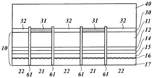
Figure la shows a base film 10 having a carrier film
11, a release layer 12 and a decorative layer 13, which
comprises a protective lacquer layer 14, a replication
lacquer layer 15, a reflection layer 16 and an adhesive
layer 17.
The carrier film 11 is preferably a PET, PEN or BOPP
film having a thickness of 6 pm to 125 pm. The release
layer and the decorative layer are then constructed
successively on the carrier film 11 by the application
of further layers. For this purpose, firstly the
release layer 12 is applied to the carrier film 11. The
release layer 12 preferably consists of a waxy material
which is softened in particular by the heat occurring
during a hot embossing process and enables the
decorative layer to be reliably separated from the
carrier film 11. The thickness of the release layer is
preferably between 0.01 pm and 1.2 pm. The protective
lacquer layer 14 is subsequently applied with a layer
thickness of between 0.5 pm and 1.5 pm. In this case,
it is also possible for the protective lacquer layer 14
to perform the function of the release layer 12 and,
accordingly, both to enable the decorative layer 13 to
be separated from the carrier film 11 and to protect
the decorative layer 13 against mechanical influencing
and environmental influences. In this case it is also
possible for the protective lacquer layer 14 to be
colored or to contain micro- and nanoparticles.
The replication lacquer layer 15 consists of a
thermoplastic lacquer into which a surface structure is
CA 02745913 2011-06-06
- 22 -
impressed by means of heat and pressure by the action
of an embossing tool. Furthermore, it is also possible
for the replication lacquer layer 15 to be formed by a
UV-crosslinkable lacquer and for the surface structure
to be impressed into the replication lacquer layer 15
by means of UV replication.
The replication lacquer layer 15 preferably has a layer
thickness of between 0.5 pm and 15 um. The surface
structure impressed into the replication lacquer layer
is preferably a diffractive surface structure, for
example a hologram, Kinegram or some other
diffraction-optically active grating structure. Such
surface structures usually have a distance between the
structure elements in the range of 0.1 pm to 4 pm.
Furthermore, it is also possible for the surface
structure to be a macroscopic surface structure, for
eample a microiens array or a blazed grating.
The reflection layer 16 is applied to the replication
lacquer layer 15 after the surface relief has been
impressed. The reflection layer 16 is preferably a
metal layer composed of chromium, copper, silver or
gold or an alloy of such metals, which is vapor-
deposited in vacuo with a layer thickness of 0.01 pm to
0.04 pm. It is also possible for the reflection layer
16 to be formed by a transparent reflection layer, for
example a thin or finely structured metallic layer or
an HRI or LRI layer (HRI = High Refraction Index; LRI =
Low Refraction Index). Such a dielectric reflection
layer consists, for example, of a vapor-deposited layer
composed of a metal oxide, metal sulfide, titanium
dioxide, etc., having a thickness of 10 rim to 50 nm.
Furthermore, it is also possible here instead of or in
addition to the layers 14 to 16, in the decorative
layer, to introduce even further layers that generate
an optically variable effect, for example a thin-film
CA 02745913 2011-06-06
- 23 -
layer system, a layer composed of a crosslinked
cholesteric liquid crystal material or a color layer.
Furthermore, it is also possible for the decorative
layer to comprise one or a plurality of electrically
conductive or semiconductor layers that realize an
electrical circuit or an electrical component, for
example an RF resonant circuit or an RFID tag. This can
involve a metallic layer, for example, which is applied
either by vapor deposition or by printing and is
subsequently reinforced by electrolytic growth. In
particular, the reflection layer 16 can simultaneously
serve as an electrically conductive layer, which, for
this purpose, can likewise be subsequently reinforced
electrolytically. Furthermore, the decorative layer 13
can comprise one or a plurality of layers composed of a
magnetic material or an electroluminescent material.
The adhesive layer 17 is subsequently applied with a
layer thickness of approximately 0.3 mm to 0.5 um. The
adhesive layer 17 preferably consists of a thermally
activatable adhesive and is applied to the layer 16
over the whole area, for example by means of a doctor
blade.
As indicated in figure la and figure lb, the base film
10, and hence also the decorative layer 13, has two
first partial regions 21 and a second partial region 22
enclosing the first partial regions 21. In this case,
the first partial regions constitute that part of the
decorative layer which is to be transferred as a
security element onto a target substrate, for example a
security document.
Preferably, the relief structure impressed into the
replication lacquer layer 15 is chosen such that it
generates a predefined optically variable information
item in the first partial regions 21. The surface
structure impressed in the first partial regions 21
CA 02745913 2011-06-06
- 24 -
thus preferably differs from the surface structure
impressed into the replication lacquer layer 15 in the
partial region 21. Furthermore, the reflection layer 16
is provided in a patterned fashion and partially, and
provides a second predefined information item in the
first partial regions 21. Preferably, the patterned
configuration of the reflection layer 16 in the first
partial regions 21 thus also differs from that in the
second partial region 22. Preferably, the reflection
layer 16 is not provided in the second partial region
22. The optional further optically active layers of the
decorative layer 13 are also preferably shaped in a
manner maintaining register with the partial regions 21
and provide further information items in the partial
regions 21, such that the shaping of this layer in the
first partial regions 21 likewise differs from that in
the second partial region 22.
Furthermore, it is also possible for a multiplicity of
first partial regions to be provided, which are
enclosed by a continuous second partial region
enclosing the first partial regions. This is shown by
way of example in figure lc, which illustrates a base
film 10' with first partial regions 21' and a second
partial region 22'.
In a first step illustrated in figure 2, an adhesive
layer 30 is applied to that side of the carrier film 11
which lies opposite the decorative layer 13. In this
case, the adhesive layer 30 is applied to the carrier
film 11 over the whole area. Furthermore, it is also
possible for the adhesive layer 30 to be applied to the
carrier film 11 only partially, for example in the form
of a point grid, as has already been described above.
The adhesive layer 30 is a UV-activatable adhesive. The
adhesive that can be used for the adhesive layer 30 has
the following composition, for example:
CA 02745913 2014-12-02
- 25 -
Dicyclopentyloxyethyl methacrylate 50 - 60%
2-hydroxyethyl methacrylate 8%
Trimethylolpropane triacrylate 40 - 30%
(3-(2,3-epoxypropoxy)propyl)trimethoxysilane 1%
Irgacure 184 (CIBA) 1 - 2%
The adhesive layer 30 is applied to the carrier film 11
with a layer thickness of 0.1 pm to 10 um by means of a
printing method, by means of pouring or by means of a
doctor blade.
In a second second step illustrated in figure 3, a
carrier film 40 is applied to the adhesive layer 30.
The carrier film 40 is a transparent plastic film,
which preferably consists of PET, PVC, PEN or BOPP film
and has a layer thickness of 6 pm to 250 pm.
In a third step illustrated in figure 4, a first region
of the adhesive layer 30 is activated by exposure. For
this purpose, the film structure consisting of the
carrier film 40, the adhesive layer 30, the carrier
film 11, the release layer 12 and the decorative layer
13, as shown in figure 4, is exposed with UV light 5 in
the region 31. For this purpose a collimated light
source is used which is on that side of the carrier
film 40 which faces away from the carrier film 11, and
is at a distance from the carrier film 40. In this
case, an exposure mask is arranged in the beam path
between the light source and the adhesive layer 30,
said exposure mask covering the region 32 and thus
enabling selective exposure of the region 31. The
exposure source and the exposure mask are preferably
part of a drum exposure device over which the film body
shown in figure 4 is guided. As shown in figure 4, the
exposure mask is in this case shaped and arranged such
that the region 31 largely covers the first partial
regions 21 and is positioned within the scope of a
CA 02745913 2011-06-06
- 26 -
register tolerance of preferably 0.1 mm to 2.0 mm with
respect to the first partial regions 21.
In the region 32, the adhesive layer 30 is not exposed
by UV light and therefore not activated.
In a fourth step illustrated in figure 5, the
decorative layer 13, the release layer 12 and the
carrier film 11 are severed along the boundary lines
defining the first partial regions 21 and separating
the first partial regions 21 from the partial region
22. These layers are preferably severed by means of a
stamp that introduces corresponding cutouts 61 into the
film body consisting of the layers 30 and 17 to 11. As
indicated in figure 5, it is also possible in this case
for the stamping depth to be chosen such that the
carrier film 40 is partly severed as well. Furthermore,
it is also possible for the carrier film 11 not to be
severed completely but rather only partly. This can be
done firstly in the form that the regions in which the
carrier film 11 is completely severed or not severed
alternate along the boundary line, or that the carrier
film 11 is not severed in its entire thickness, but
rather only for example in 80% of its thickness.
In a fifth step, that part of the base film 10 which
comprises the partial region 22 is removed from the
carrier film 40, wherein, on account of the adhesive
layer 30 activated in the region 31, the base film
still adheres to the carrier film 40 in the first
partial regions 21 and remains on the carrier film 40.
After putting on the "grating" this results in the
multilayer body 1 shown in figure 6, which multilayer
body can be used as a security element or as a transfer
film for applying a security element to a target
substrate. As illustrated in figure 6, in this case
residues of the non-activated material of the adhesive
layer 30 remain on the carrier film 40 in the region
CA 02745913 2011-06-06
-27-
32. If appropriate, subsequent exposure of the film is
effected.
As illustrated with reference to figure 7 and figure 8,
the multilayer body 1 can be used as a transfer film
for applying a security element 23 to a target
substrate 70. For this purpose, the multilayer body 1
is placed onto the target substrate 70 and the adhesive
layer 17 is activated in a first partial region by
means of a correspondingly shaped hot embossing die 71.
The multilayer body comprising the carrier film 40, the
adhesive layer 30 and the carrier film 11 is
subsequently removed from the applied region of the
decorative layer 13 such that the security element 23
remains on the target substrate 70, as shown in
figure 8.
7