Note: Descriptions are shown in the official language in which they were submitted.
CA 02746380 2011-06-27
DEVICE AND METHOD FOR DRIVING LEDS
FIELD OF THE INVENTION
The present invention relates to a device and method for driving light
emitting diodes
(LEDs) using = switched mode power supply configuration. The invention is
particularly suited for the design of a LED current controller and will be
described in
this context.
=
BACKGROUND TO THE INVENTION
0 The following discussion of the background of the invention is
intended to facilitate
an understanding of the present invention. However, it should be appreciated
that the
discussion is not an acknowledgement or admission that any of the material
referred ,
to was published, known or part of the common general knowledge in any
jurisdiction
as at the priority date of the application.
Light Emitting Diodes (LEDs) are often driven by controller circuits to
fulfill one or
more objectives. As LEDs are sensitive to current and voltage fluctuations,
one of the
most important objectives for LED controller circuits is to provide
appropriate current
to drive the LEDs under supply voltage or load variations. '
Pulse-Width Modulation (PWM) based controllers have been developed to provide
appropriate current , to LEDs under supply voltage/load variations. Most PWM
controllers are switched-mode based controllers involving the use of
electronic
= 20 switches such as MOSFET as a means for regulating the current input to
the LEDs.
Fig. 1 illustrates a typical buck-boost LED controller used for an isolated AC
application. The current driver circuitry is based on an analog PWM
controller, which
includes the use of current feedback resistors 13; opto-couplers 14; and
polarized
capacitors 12. The current driver circuitry further includes an analog PWM
controller
15.
The PWM based controller circuit has several disadvantages listed as follows:
= 1
CA 02746380 2011-06-27
= As the current-sense feedback resistors 13 are in the current path of the
power
MOSFET and the LEDs, it dissipates a lot of electrical energy. This is a loss
of
electrical energy as the feedback resistors 13 consume electrical energy
(which is
dissipated as heat) which is not producing useful work. Moreover, such
feedback
resistors 13 are typically power resistors which generate considerable heat
and
generally require thicker 'copper design when implemented on a printed circuit
board (PCB). This increases the overall cost of implementation.
= The lifetime of the polarized capacitors 12 is typically much shorter
than the
lifetime of the LEDs. When one or more polarized capacitors 12 break down,
they
lead to short circuits which may further cause the malfunctioning of the
driver
circuitry. Such malfunctioning is likely to shorten the lifetime of the LEDs
due to
a cascading malfunctioning effect.
= The polarized capacitors 12 further introduce phase differences in the
circuit-
which decreases power factor and the overall useful electrical power
efficiency.
= The opto-couplers 14 are typically expensive electrical components which
will
increase the overall cost of implementing the LED controller.
In addition to the above disadvantages, the Applicant submits that generic PWM
controllers (whether analogue or digital) work based on fixed/narrow
frequencies
range and does not ensure that the controller is working in a discontinuous
mode
0 20 when the operating frequency changes.
It is thus an object of the invention to overcome, or at least ameliorate in
part, one or
more of the aforementioned problems.
SUMMARY OF THE INVENTION
Throughout this document, unless otherwise indicated to the contrary, the
phrase
"comprising", "consisting of', and the like, are to be construed as inclusive
and not
exhaustive.
14*
2
CA 02746380 2013-10-22
=
,
In accordance with a first aspect of the present invention there is a device
for providing electrical
current to at least one Light Emitting diode (LED) via a switch mode power
converter
comprising: at least one Integrated Circuit (IC), the IC programmable using a
hardware
description language; an electronic switch configurable to have a switching
time period; an
Analogue to Digital converter (ADC), the ADC configured to provide a digitized
voltage input; a
voltage comparator, the voltage comparator configured to obtain a discharge
time of an inductive
element of the switch mode power converter at each switching time period;
wherein in operation,
the at least one IC is configured to obtain the digitized voltage input, the
discharge time of the
inductive element, the desired electrical current, a reference constant value,
and the switching
time period of the electronic switch as inputs and therein calculate the
switch-on time of the
electronic switch at each switching time period, so that the switch-on time of
the electronic
switch regulates the electrical current flowing into the at least one LED.
Preferably, the at least one IC is an application-specific integrated circuit
(ASIC).
Preferably, the switch-on time of the electronic switch is calculated
according to the following
formula:
'OUT * T
TON -
K * VIN * TOE!.
Where TON is the switch-on time of the electronic switch, 'Om- is the desired
electrical current; T
is the switching time period of the electronic switch; K is the reference
constant value; TOFF is the
discharge time of the inductive element of the switch mode power and VIN is
the digitalized
voltage input.
Preferably, for an isolated alternating current (AC) fly back configuration
having the inductive
element as a transformer isolating the at least one LED at the secondary end
of the transformer,
the reference constant K is calculated according to the following formula:
1
K= _____________________________________________
2 * VL, *L2
3
CA 02746380 2011-06-28
=
=
I
= . PCMG2010/000212
Received 13 May 2Q11
=
viherein Li is the inductance value of the primary winding of a tansfonner and
14 is
. . the =inductancre value of the soionclary winding of the transibmer.
Preferably, the ,
= . transibrmer is a planar icansfbrmer.
. =
Alarmadvely, thr -a non-isolated direct current (PC) iv back configuration,
the .
, 5 redeem. constant valueKisoalculated according te the rellowinf
*mile
=
1
= L; =
=
. .
:wherethi 14 is the inductance value of the inducfive element in the fly back
,
= configiradon;
, = , =
. =
Preferably, the value of Am is updeted at etch. tbno period based on compering
an
value A=with a value ik.the formulae of A and B are repectiVelyt
.
=
= A= Nin4.4100Tory, and
. =
B-41/1CrIourstirrw+ Tow + Tama
=
=
=licheral Tama is the time after the .discharge time Of the inductive elemect
. . ,
=
001 the 1U15 and the switching One period of deotronic
switch is the =
= = . 15 senurretion. Of To& Topa and TnaLe;
=
=
, 'tech that when the V*Illo of A ialgrater than 11, the veto of
To4 is decreased by a
= predetermined number of clock cynics: when the value of A in. smaller
than B, the.
=
value of TON is increased by the predetermined umber of cloak cycles; mud whoa
the =
- = value of A is equalschange is made to To*
=
=
Prefinb.ly, the (levies tee/wed for adjusimet ofthe .eleotricei cared as a
traction =
= of umperature by mums of a thertnistor potddoned at the junction of each
LED the
= device farther configured to update. the electrical enured cmtput via
updating the
=. predetermined inimbei of clock cycles.
=
=
=
=
= =
1. 4
= =
. = =
. = = = =
=
=
. . =
= =
=
=
= =
=
= = Ammded Shest
= .
IPA/AU ,
=4.
=
. = =
CA 02746380 2013-10-22
Preferably, the electronic switch is a metal¨oxide¨semiconductor field-effect
transistor
(MOSFET), and in operation, the MOSFET is configured to work in a
discontinuous mode.
Preferably, the ADC, voltage comparator and oscillator are integrated into the
IC.
In accordance with a second aspect of the present invention there is a method
for providing
electrical current to at least one Light Emitting Diode (LED) via a switch
mode power converter
comprising the steps of:
(i) obtaining (a) a digitized voltage input; (b) a switching time period of an
electronic switch;
(c) a discharge time of an inductive element of the switch mode power
converter; (d) the
desired value of the electrical current; and (e) a reference constant (K) as
inputs and
(ii) calculating a switch-on time of the electronic switch at each switching
time period;
(iii) regulating the electrical current flowing into the at least one LED at
each switching time
period based on the switch-on time of the electronic switch; and
(iv) repeating steps (i) to (iii) for each switching time period.
Preferably, the switch-on time of the electronic switch is calculated
according to the following
formula:
* T
TON -
K * VIN * T 0õ
Wherein 'OUT is the desired electrical current; T is the switching time period
of the electronic
switch; K is a reference constant; TOFF is the switch-off time of the
electronic switch at each
switching time period and VIN is the digitized voltage input.
Preferably, for an isolated alternating current (AC) source input having a
transformer isolating
the at least one LED to the secondary end of the transformer, the constant
gain value K is
calculated according to the following formula:
5
CA 02746380 2011-06-28
= =
PCTAG2010/000212 .
Received 13 May 2011
= =
Le =
= 277-47aL1 =
=
wherein Li is Ste inductenea value of the primary winding of a transibrater
sad 1.2 in
the inductanee value of the secondary winding of the transfixmer.
=
Alternatively, br a non-ilolated direct current (DC) Arlin& configuration, the
' . 5 reference commit is -calculated. according to the tbRowing
lormuls
. .
= =
. ,
=
L3 =
=
wherein Li b the inductance' value of an inductive edema in the fly-back
. configuration.
Preibrabiy, the nine of=ToN is updated based on ampere* a value A with a
vali4e ;
i0 the tbrasulas of A and B are respectively:
= =
=
= . IllTosnoire; lad =
= =
== 8= (1/1()loOr(row .1. Tow+ Tcoac) =
. .
= =
=
, 'Wherein Tcf-ag ia. the time after. the discharge We of the
toduativi element to .
=. compute .the fort:tole and the switching time period a. the elects:tele
switch is the
=
= 15 ismsnationOtTec, Top aid TcALd;
=
. . =
such thet *hen the veluc of A ii greater than B, die value of Teti fa
decreased by' a
pedetcemined number of clock' cyclea; when the value of A is smaller then B,
the
value of To, hi increased by the predetermined number of clock cycles; end
Nihon the
= value (Okla equais to B, IIC) change is rnade to To*
= =
=
20 =
=
= =
SRIIF DESCRIPT/ON 01? 1111E DRAWDRA = -
The taming invention will be described with rake= to the followhy drawing; of
. =
=
=
=
' =
. =
= = Amended sent =
= IPPA/AU
.
=
=
CA 02746380 2011-06-27
=
Fig. 1 illustrates a prior art LED current controller circuit
Fig. 2 illustrates a configuration of the LED driver circuit in accordance
with the first
embodiment of the invention for isolated alternating current (AC) application.
Fig. 3 illustrates a configuration of the LED driver circuit in accordance
with the
second embodiment of the invention for non-isolated direct current (DC)
application.
Fig. 4 illustrates a flow chart for implementation of a digital algorithm in
accordance
=
with the first and second embodiment of the invention.
Fig. 5 illustrates possible waveforms at the gate and drain of the electronic
switch
0 (MOSFET) in accordance with the first and second embodiment
embodiments of the
invention.
Other arrangements of the invention are possible and, consequently, the
accompanying drawings are not to be understood as superseding the generality
of the
preceding description of the invention.
DETAILED DESCRIPTION OF THE INVENTION
=
In context of the description, the term 'current' will generally be understood
to mean
=
'electrical current' unless otherwise indicated.
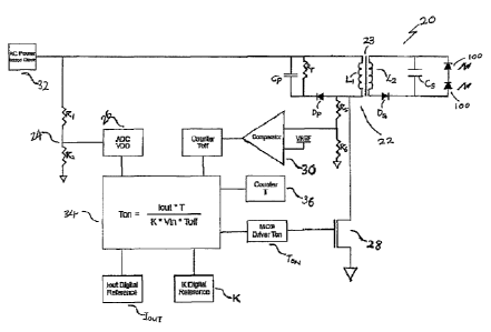
0 In accordance with the first embodiment of the invention shown in
Fig. 2 there is a
device for providing electrical current to at least .one Light Emitting diode
20, The
device is a LED driver 20 for an isolated alternating current (AC)
application. The
LED driver comprises transformer 23, fly-back converter 22, voltage divider
24,
Analog-to-digital converter (ADC) 26, electronic switch 28, voltage comparator
30,
bridge rectifier 32, Integrated circuit (IC) 34 and an electronic oscillator
36.
= Transformer 23 is an isolation transformer. Transformer 23 decouples a
LED load 100
from the rest of the circuitry. Each LED 100 is connected in series with other
LEDs
100. The winding ratio of transformer 23is configured according to the number
of
LEDs in LED load 100. . Transformer 23 may be a planar transformer or other
low-
loss transformers as known to a person skilled in the art.
7
7,S7
- r ,4
CA 02746380 2011-06-27
Resistor Rp and capacitor Cp are connected in a parallel configuration with
the .
=
primary end of the transformer 23. A diode Dp is connected to the Resistors
Rp,
capacitor Cp, and the transformer 23. The conducting end of the diode Dp is
connected in a series configuration to the primary end of the transformer 23.
The non-
conducting end of the diode Dp is connected in series configuration to the
resistor Rp
and capacitor Cp.
A capacitor Cs is connected in parallel to the secondary end of the
transformer 23. A
diode Ds is connected to the secondary end of the transformer 23 and the
capacitor
Cs. The conducting end of the diode Ds is connected to the secondary end of
the
transformer 23 in a series configuration. The non-conducting end of the diode
Ds is
0 connected to the capacitor Cs in a series configuration. The LED
load 100 is
connected in a parallel configuration to the capacitor Cs.
Voltage divider 24 comprises a series of standard resistors. For illustration,
voltage
divider 24 is represented using standard resistors R1, R2. For an AC supply
voltage of
230 VAC, the resistance value for R1 is about 300k0 and for R2 is about
2.2kSZ.
During operation, the voltage between R1 and R2 is tapped by ADC 26. The
tapped
voltage is converted to a digital value VDD. One end of R2 is connected to
electrical
ground.
". The ADC 26. is suited to operate in the range of 50 to 120 Hi. In order
for the
embodiment to work, the minimum resolution of the ADC 26 should- be 8-bit. The
0 digitized voltage of the ADC 26 may also be used as an under-
voltage security lock.
Electronic switch 28 is typically a power transistor. In this particular
embodiment,
electronic switch 28 is a MOSFET. The drain of the electronic switch 28 is
connected
to the conducting ,end of the diode Dp. The gate of the electronic switch 28
is
connected to the output pin of the IC 34, and the source of the electronic
switch 28 is
connected to the electrical ground.
Voltage comparator 30 is connected to the primary end of the transformer 23
via a
resistor R5. Resistor R5 is in turn connected in a series configuration with
resistor R6.
When in operation, voltage comparator 30 obtains the voltage between resistor
R5 and
8
- et..
CA 02746380 2011-06-27
resistor R6. The obtained voltage is compared with a voltage reference VDEF.
VDEF is
typically configured to be the same value as VDD. Voltage comparator 30 is
typically
(but not limited to), an operational-amplifier.
The bridge rectifier 32 is configured to provide a rectified output from the
AC mains.
The AC mains may be either 110 VAC or 230 VAC.
The IC 34 is typically an Application Specific Integrated Circuit (ASIC). In
this
regard, it is to be appreciated that ADC 26, voltage comparator 30, electronic
oscillator 36 may be integrated with IC 34. In addition, IC 34 may further
comprise
Regulators, Power-on-reset, MOSFET driverõ One-time programmable (OTP)
o10 memory, EEPROM, Flash and/or other programmable memory blocks as known
to a
person skilled in the art. IC 34 may be programmed using hardware description
language (HDL) such as Verilog,, VHDL, or other hardware description language
as
known to a person skilled in the art.
The IC 34 is programmed and configured to receive five inputs; i.e.
=
= 15 (a.) A reference constant K;
= (b.) Desired reference current lout
=
(c.) The digitized voltage value VDD -obtained from the ADC 26;
O (d.) A time value ToFF of the discharge of the core of transformer
23 measured
through voltage comparator 30; and
20 (e.) A switching period T (i.e. the switching period of the electronic
switch 28) as
illustrated in Fig. 5.
In relation to the switching period of the electronic switch 28, the
electronic oscillator
36 generates an operating frequency of 20 MHz, i.e. at a time period of 50
nano
seconds. The switching time of the switch mode power supply (SMPS) is related
to
25 the on/off of the electronic switch 28. In the context of this
embodiment, the
switching time of the SMPS ranges from 30 kHz to 300 kHz.
9
Erc.-T.'
CA 02746380 2011-06-27
Using the received five inputs, the IC 34 computes an output TON to drive the
gate of
the electronic switch 28 in accordance with formula 1.
* T
ToN (1)
K
Where TON is the switch-on time of the electronic switch 28, lour is the
desired
reference current; T is the switching time period of the electronic switch 28;
K is the
reference constant; TOFF is the discharge time of the transformer 23 and VN is
the
digitalized voltage input
The reference constant K is calculated based on the inductance value of the
primary
0 and secondary windings of the transformer 23 as described in
formula 2.
=
1
K-
2*.s/LI *L2 - (2)
where L1 is the inductance value of the primary windings of the transformer 23
and
L2 is the inductance value of the secondary windings of the transformer 23.
The value
of reference K is stored in a memory within the IC 34, the memory may be one-
time
programmable (OTP), flash or EEPROM. Alternatively the reference K may be
hardcoded in the formula, i.e. the value of reference K is stored inside the
IC 34 as
registers, in which case the K value may not be updated during operation.
0 The electronic oscillator 36 (20 MHz frequency, 50 ns period) is
coupled with an
internal 10 bit counter to count TON and TOFF. The 10 bit counter translates
to 1024
clock cycles before overflow). This means that with the 10 bit internal
counter, the
1024 clock cycles may be counted within 5Ons * 1024 ----'- 51.2us. Hence, the
counter is
capable for counting between 19.53125 kHz up to 20 MHz. It is to be
appreciated
that the switching time T of the electronic switch 28 of 30 kHz to 300 kHz
falls
within the above range.The digital reference current lour fixes the desired
output
current to drive the LEDs. The value of digital reference current 'ou'r may be
either
stored in the memory of IC 34 or hardcoded in the formula, in which case the
digital
reference value lour may not be updated during operation.
!Slfr
CA 02746380 2011-06-28
F =
=
=
= = PCT/S02010/000212
=
= Received 13 May 2011
=
=
. The enabodiment = will next be described in the context of its.
operant& As an =
illustration (aid not moat m be mralusive), a voltage input-of 230VAC is
mitered to
drive the LED driver 20. -Melee LEDs 100 am connected is series with esch
other,
The eighteen LED s 100 form the 1210 load.
Fig. 5 illustrates typical voltage-time waveibrms et the gate and drain of the
olectomic
Switch 28 when the LED .driver 20 bin poetic& A voltage ovashoot at the diain
of
electronic switch 281* motored. The voltage overshoot is Proportional to the
voltage
aeons the LEDs 100. The voltage overshoot value is used to Dieu= tie tinns of
core
= discharge tvgy =Mg the voltage comparator 30 and a digital counter. The
value of
Toro la measured based on the thin of the care discharge of the primary end of
the
=
transformer 23. =
=
=
During operation, VRIF is configused to be the mitt voltage :exotic of the
input
Voltage Vali AI sampled by the ADC 24. Such a configuranon murex that the
electronic snitch 28 is consistently working in discontinuous mode. = -
"
. .
The value of Trois fine,tuned iteratively in acoardance to the now chart
illestrated in.
Pig. 4 such that over a period (of clock cycled), the electdcal mutant tiowhig
into the
=
LED load 100 a:Oaten hv Wasting Tod. The steps are deicribed hi the flowchart.
= ste deo:died es follows: =
=
=
= The electrode
swift 281s activated for Tel./ time. (Step 60) = =
= . 20 The'
Tdyrtiming is computed based on the voltage comparator 30 and digital mimetic
=
= (StuP 62) = . .
. .
A value Vitr(VDeVic) is obtaiied tom the ADC 36(digi1ized value) (Step 64)
=
Foment% (3)1* plinputed as Wows; (Step 66) .
A a. Vol * Tem *Tort (3)
=
=
Itansula (4) is computed ma &lbws: (Step 68)
,
=
=
= -5.(ing)* lour
111 (Tom + Ton + Tour) (4) =
= =
=
=
=
=
= no/ o== =====
===========61 =11
= = =
=
= .
= .
=
= =
=
= Amended Shea
=
1?EA/AU
=
=
=
=
CA 02746380 2011-06-27
=
wherein TCALC is the time after the discharge to compute the formula.
such that the switching period T of the electronic switch 28 is the surmnation
of TON,
ToFF and TCALC.
The actual implementation takes approximately 128 clock cycles.
The value of A and B are compared (Step 70).
If A is greater than B, i.e. A> B, then TON is adjusted to TON¨ N for the next
time
period T (Step 72).
a If A is smaller than B, i.e. A <B, then TON is adjusted to TON + N
(Step 74).
In the situation where A is equals to B, there is no updating of TON and TON
remains
= 10 Unchanged (Step 76).
= The value N is an adjustment value. N is the increment or decrement of
the switch-on
time TON of the MOSFET. The adjustment value N forms part of the feedback loop
=
,for stabilizing current Tour under supply variation. The value of N typically
ranges
between 1 and 128 number of clock cycles.
It is to be appreciated that for different differences of A and B, different
values of N
are used.
0 It is to be farther appreciated that A and B is computed separately
due to the
complexity of performing hard-coded division, which is time-consuming and
inefficient for this application. To overcome the problem, algebraic
manipulation is
used to compute the formulas (3) and (4) and therein compare the results
between A
and B.
The process Step 60 to 76 repeats itself until the circuit is switched off or
according to
other terminating condition as known to a person skilled in the art.
The ToFF value may further be configured for short circuit protection of the
LED load
100. For the purpose of short circuit protection, the ToFF value is compared
with a
12
CA 02746380 2011-06-27
short circuit reference value ToFF, sc. If a short circuit is present on the
secondary
winding of the transformer 23, where the LED load 100 is, the TOFF value will
be
shorter than the short circuit reference value TOFF, sc, thereby activating
the short
circuit protection.
The Applicant has discovered that the use of the ASIC and the implementation
of
formula (1) to (4) are independent from the number of LEDs in the load. The
implementation of the ASIC further omit the need for polarized capacitors on
the
main power supply, polarized capacitors with larger capacitance on the
secondary
windings of transformer 23, feedback power resistors on the MOSFET and on the
LED chain/load. The total efficiency (as well as power factor correction) of
the
0 system will thus increase as majority of the elebtrical power will
be transferred to the
LEDs instead of to the feedback resistors and capacitors. In addition, the
cost of
implementing the circuitry is typically lower than the prior art circuitry as
described
in Fig. 1, as the components used generally lower in cost as compared to
specific
components such as opto-couplers 14 (thereby omitting the need for voltage
feedback'
on the secondary end of transformer 23) and polarized capacitors.
In the above example, with eighteen LEDs (each LED 100 having a forward
voltage
of 3.2V) and an input of 230 VAC and a reference output current Iour of 350
milli-
amperes (mA), an efficiency of as high as 94% is achieved. This is based on
obtained
demo-board simulation results, where the system power consumption is 21.5W.
The
total LED power consumption is 20.16 W such that the efficiency is 20.16
divided by
21.5, i.e. 93.8 %.
In addition, for the purpose of short circuit protection, if one LED 100 is
shorted the
formulas (1) to (4) are capable of adapting the value of TON to provide the
right
current to the working LEDs via the feedback mechanism described in Step 60 to
76.
The driver 20 is thus independent from the number of LEDs present on the
secondary
end of the transformer 23 (i.e. the load side).
An additional security option is done computing the TON multiplied by the VIN
value.
In order not to saturate the transformer core LI, L2 this value must be under
a digital
13
CA 02746380 2011-06-27
threshold value TommAx. The digital threshold value TON,MAX is calculated as
Formula (5), assuming that the core saturates at 0.3 Tesla:
TommAX * 0.3 * A8) / (\TIN) (5)
Where Np is the number of primary windings, A5 is the effective area of the
transformer, \TIN is the input voltage.
In accordance to the second embodiment of the invention as shown in Fig. 3
there is a
device for providing electrical current to at least one Light Emitting diode
120. The
device is an LED driver 120 for a non-isolated DC application. The LED driver
comprises fly-back converter 122, voltage divider 124, Analog-to-digital
converter
(ADC) 126, electronic switch 128, voltage comparator 130, DC power supply 132
and
an Integrated circuit chip (IC) 134 and electronic oscillator 136.
Fly-back converter 122 comprises a diode 121 connected in a series
configuration
with inductor 123 and capacitor 125. Inductor 123 and capacitor 125 are
configured to
be in a parallel configuration with the LED load 200. Each LED 200 is
connected in
series to other LEDs 200. The conducting end of the diode 121 is connected to
the
inductor 123. The non-conducting end of the diode 121 is connected to the
capacitor
125.
. . .
Voltage divider 124 comprises a series of standard resistors. For
illustration, voltage
0 divider 124 is represented using standard resistors R3, R4. The
voltage between R3
and R4 is tapped by ADC 126 during operation. At a DC voltage of 12V, the
value of
R3 and R4 are about 47162 and 4.7k1 respectively. One end of R4 is connected
to
electrical ground.
The ADC 126 operates in the range of 50 to 120 Hz. In order for the embodiment
to
work, the minimum resolution of the ADC 126 is 8-bit. The digitized voltage of
the
ADC 126 may be used as an under-voltage security lock. The tapped voltage
between
R3 and R4 is converted to a digital value VDD.
Electronic switch 128 is typically a power transistor. In this particular
embodiment,
electronic switch 128 is a MOSFET. The drain of the electronic switch 128 is
14
E t;27 7
CA 02746380 2011-06-27
:
=
connected to the conducting end of the diode 121 and the inductor 123. ,The
gate of
the electronic switch 128 is connected to the output pin of the IC 134, and
the source
of the electronic switch 128 is connected to the electrical ground.
Voltage comparator 130 compares the voltage obtained at the drain of the
electronic
switch 128 with a voltage reference VREF. Voltage comparator 130 is typically
(but
not limited to), an operational-amplifier.
=
The DC power supply 132 is configured to provide a DC output to the circuit.
The DC
output may range from 3V to 400V.
The IC 134 is typically an Application Specific Integrated Circuit (ASIC). In
this
0 10 regard, it is to be appreciated that ADC 126, voltage comparator
130, electronic
oscillator 136 may be integrated with IC 134. In addition, IC 134 may further
comprise regulators, Power-on-reset, MOSFET driver, UT? memory, EEPROM,
Flash and/or other programmable memory blocks as known to a person skilled in
the
art. IC 134 may be programmed using hardware description language (HDL) such
as
Verilog, VHDL, or other hardware description language as known to a person
skilled
in the art. -
The IC 134 is programmed and configured to receive five inputs; i.e.
(a.) A reference constant K;
0 (b.) Desired reference current
(c.) the digitized voltage value VDD obtained from the ADC 126;
(d.) A time value Tc=FF of the core discharge of the inductor 123; and
(e.) A switching period T, the switching period of the electronic switch 28
obtained
from electronic oscillator 136.
The electronic oscillator 136 generates an operating frequency of 20 MHz, i.e.
a time
period of 50 nano seconds. The switching time of the switch mode power supply
-
.74kr -kt: sat
CA 02746380 2011-06-27
(SMPS) is related to the on/off of the electronic switch 128. In the context
of this
embodiment, the switching time of the SMPS ranges from 30 kHz to 300 kHz.
Using the received five inputs, the IC 134 computes an output TON to drive the
gate of
the electronic switch 128 in accordance with formula I.
The reference constant K is calculated based on the discharge time of the
inductor 123
as described in formula 6.
L3 (6)
0 where 1,3 is the inductance value of the inductor 123. The reference
K is a digital
value and could be stored in a memory within the IC 134, the memory could be
OTP, =
flash or EEPROM. or hardcoded in the formula, in which case the digital value
is
" stored inside the ASIC 134 as registers; thus the digital value may not be
changed
during operation.
The electronic oscillator 136 (20 MHz frequency, SO ns period) is coupled with
an =
internal 10 bit counter to count TON and ToFF. The 10 bit counter translates
to 1024
" 15 clock cycles, before overflow). This means that with the 10 bit internal
counter, the
1024 clock cycle may be counted within SOns * 1024 51.21.ts. Technically
speaking,
the counter is capable for counting between 1.53125 kHz up to .20 MHz. Thus
the
switching time T of the electronic switch 128 of 30 kHz to 300 IcHz falls
within the
0 above range.
The embodiment will next be described in the context of its operation.
Fig. 5 illustrates typical voltage-time waveforms at the gate and drain of the
electronic
switch 128 when the LED driver 120 is in operation. A voltage overshoot at the
drain
of electronic switch 128 is measured. The voltage overshoot value is used to
measure
the time of core discharge ToFF using the voltage "comparator 130 and a
digital
counter. The value of TOFF is measured based on the discharge time of the
inductor
123. This is easily obtained via various methods as known to a person skilled
in the
art
16
-c
CA 02746380 2011-06-27
=
During operation, VREF is configured to be the same voltage reference of the
input
voltage VDD as sampled by the ADC 126. This configuration ensures that the
electronic switch 128 is consistently working in discontinuous mode.
The value of TON is fine tuned iteratively in accordance with the flow chart
as
illustrated earlier in Fig. 4. The process Step 60 to 76 repeats itself until
the circuit is
=
switched off or according to other terminating condition as known to a person
skilled
in the art.
The ToFF value may further be configured for short circuit protection of the
LEDs ZOO.
Tn this regard, the ToFF value is compared with a short circuit reference
value ToFF,SC.
0 10 If a short circuit is present on the secondary winding of the
transformer 23, where-the
LEDs 200 are, the ToFF value will be shorter than the short circuit reference
value,
thereby activating the short circuit protection.
The digital reference lour fixes the desired output current to drive the LEDs.
The
value of digital reference IouT is stored in the memory of IC 134 or hardcoded
in the
formula.
During operation, the value of TON is fine-tuned iteratively in accordance to
the flow
chart illustrated in Fig. 4 such that over a period (of clock cycles), the
electrical
current flowing into the LED load 100. is regulated by adjusting TON. The
steps .60 to
74 are described as mentioned earlier. Steps 60 to 74 repeats itself until the
circuit is
0 20 switched off or according to other terminating condition as known
to a person skilled
in the art.
The TOFF value may further be configured for short circuit protection of the
LED load
200. For the purpose of short circuit protection, the TOFF value is compared
with a
short circuit. reference value TOFF, sc. If a short circuit is present on the
inductor 123,
where, the LED load 200 is, the ToFF value will be shorter than the short
circuit
reference value ToFF, sc, thereby activating the short circuit protection.
The digital reference lour fixes the desired output current to drive the LEDs.
The
value of digital reference low may be either stored in the memory of IC 134 or
17
8C11, 14c nr stic:
CA 02746380 2011-06-27
"
hardcoded in the formula, in which case the digital reference value Iotyr may
not be
updated during operation.
In addition, for the purpose of short circuit protection, if one LED 200 is
shorted the
formulas (1), (3), (4), (6) are capable of adapting the value of TON to
provide the right
current to the working LEDs via the feedback mechanism described in Step 60 to
76.
The driver 120 is thus independent from the number of LEDs 200 present.
An additional-security option is done computing the TON multiplied by the VIN
value.
In order not to saturate the inductor 123 this value must be under a digital
threshold
value TONMAX. The digital threshold value TON, is
calculated as illustrated in
0 10 Formula (5), assuming that the core saturates at 0.3 Tesla:
With respect to both the embodiments, the Applicant observes that as the
current is
adjusted iteratively and based on the implementation of the ASIC programming,
it is
easy to dim the LED loads 100, 200 using the present circuitry without
additional
components. Thus, it is to be. appreciated that dimming may be achieved via
adjusting =
the current reference value Iour.
It is to be further appreciated that if a user wishes to switch off the device
under both
the embodiments as described, he may simply do so by inputting the current
reference
- value 'our to 0. The same user may switch on the device if he put a
different value
other than 0 in the lour register.
0
Further, the drivers 20, 120 may be configured for direct monitoring and
adjustment
of current as a function of temperature. In this regard, a thermistor may be
positioned
=
at the junction of each LED so that the controller may be adapted to auto
update a
different current output (via updating the value of N) for the LED loads 100,
200
based on the junction temperature sensed. This ensures that the LEDs 100, 200
are not
over heated. Such a strategy will lengthen the life span of the LEDs 100, 200.
The above feature may be easily implemented via an additional enable pin on
the
ASIC 34, 134 as known to a person skilled in the art.
18
CA 02746380 2011-06-27
By way of an example of the thermistor-based monitoring, if there are five
white
LEDs and one red LED connected in a series configuration, the thermistor may
be
positioned adjacent to the red LED (due to the fact that the red LED has the
lower
critical temperature as compared to white LEDs). Care should however be taken
such
that the red LED is positioned at a location where heat dissipation could take
place
readily. In this way, as soon as the critical temperature of the red LED is
reached, the
IC (ASIC) 34, 134 decrease the current to the LED load.
For illustration, when the junction temperature of the red LED reaches 60
degree
Celsius, the IC 34, 134 will adjust the current- to decrease by 10% (e.g. 300
mA).
When the junction temperature of the red LED reaches 65 degree celsius, the IC
34,
0 134 will adjust the current to decrease by 30% (250 mA); and when
the junction
temperature of the red LED is decreased to 55 degree Celsius, the IC 34, 134
will
resume the current to full load (350 mA).
It should be appreciated by the person skilled in the art that the invention
is not
limited to the examples described. In particular, the following additions
and/or
modifications can be made without departing from the scope of the invention:
= Field-programmable gate array (FPGA) can be used as an alternative to
ASIC as '
= known to a person skilled in the art.
=
= = =
= While the existing embodiments illustrate the LEDs loads 100, 200 in the
series
0 20
configuration, the LEDs loads 100, 200 may be arranged in a parallel
configuration as known to a person skilled in the art, such that the driven
current
lour is the average of the current in each single parallel chain.
= The IC 34, 134 may be further configured to have more inputs for other
purposes;
and not be limited to five inputs.
= The adjustment value N as mentioned in step 74 is the increment or decrement
of
the switch on time TON of the MOSFET and may forms part of the stabilization
filter loop. Typically the bigger the difference between A and B the bigger
the
value of N applied. As an example of a range, a ratio of 20 to 1 in terms of
clock
cycle is applied for AC/DC and from 5 to 1 in DC/DC.
19
z.!7:
CA 02746380 2011-06-27 .
=
= A Wake-up function' may be incorporated into the LED drivers 20,200 via
using
,
motion sensor with digital interface or analog threshold.
= Although the LED drivers 20, 200 as presented in the first and second -
embodiments described the invention being applied to a fly-back converter
configuration, it is to be appreciated that the IC 34, 134 and the formulas
(1) to (6)
are applicable to general switch mode power supplies including buck-boost
converters, buck converters and boost converters (both isolated AC and non-
isolated DC configurations).
= The formulas (1) to (6) is not limited to the frequency generated by the
electronic
=
0 10
oscillator 36. In general, the higher the frequency generated, the bigger the
design
required for implementation; conversely the lower the frequency, the less
precision on the current control. In this regard, 20MHz is a good compromise
= between precision and implementation.
= It should be further appreciated by the person skilled in the art that
features and
modifications discussed above, not being alternatives or substitutes, can be
combined
to form yet other embodiments that fall within the scope of the invention
described.
. . .
. . .
0
=