Note: Descriptions are shown in the official language in which they were submitted.
CA 02746926 2013-02-20
=
CAPPED STRUCTURED ORGANIC FILM COMPOSITIONS
BACKGROUND OF THE INVENTION
[0002] Materials whose chemical structures are comprised of molecules
linked
by covalent bonds into extended structures may be placed into two classes: (1)
polymers and cross-linked polymers, and (2) covalent organic frameworks (also
known as covalently linked organic networks).
[0003] The first class, polymers and cross-linked polymers, is typically
embodied by polymerization of molecular monomers to form long linear chains of
covalently-bonded molecules. Polymer chemistry processes can allow for
polymerized chains to, in turn, or concomitantly, become 'cross-linked.' The
nature
of polymer chemistry offers poor control over the molecular-level structure of
the
formed material, i.e. the organization of polymer chains and the patterning of
molecular monomers between chains is mostly random. Nearly all polymers are
amorphous, save for some linear polymers that efficiently pack as ordered
rods.
Some polymer materials, notably block co-polymers, can possess regions of
order
within their bulk. In the two preceding cases the patterning of polymer chains
is not
by design, any ordering at the molecular-level is a consequence of the natural
intermolecular packing tendencies.
- 1 -
CA 02746926 2013-02-20
.. =
[0004] The second class, covalent organic frameworks (COFs), differ
from the
first class (polymers/cross-linked polymers) in that COFs are intended to be
highly
patterned. In COF chemistry molecular components are called molecular building
blocks rather than monomers. During COF synthesis molecular building blocks
react
to form two- or three-dimensional networks. Consequently, molecular building
blocks are patterned throughout COF materials and molecular building blocks
are
linked to each other through strong covalent bonds.
[0005] COFs developed thus far are typically powders with high
porosity
and are materials with exceptionally low density. COFs can store near-record
amounts of argon and nitrogen. While these conventional COFs are useful, there
is a need, addressed by embodiments of the present invention, for new
materials
that offer advantages over conventional COFs in terms of enhanced
characteristics.
SUMMARY OF THE DISCLOSURE
[0006] There is provided in embodiments capped structured organic
films
comprising a capping unit, a plurality of segments and a plurality of linkers
arranged as a covalent organic framework, wherein at a macroscopic level the
covalent organic framework is a film.
10006a1 In accordance with an aspect of the present invention there
is
provided a structured organic film (SOF) comprising a plurality of segments, a
plurality of linkers arranged as a covalent organic framework (COF), wherein
the
framework of the SOF comprises a capping unit bonded to the framework of the
SOF via a linker group.
10006b1 In accordance with a further aspect of the present invention
there is
provided a process for preparing a capped structured organic film, comprising:
(a)
preparing a liquid-containing reaction mixture comprising: a plurality of
molecular building blocks each comprising a segment and a number of functional
groups, and a capping unit molecule; (b) depositing the reaction mixture as a
wet
film; and (c) promoting change of the wet film to form a dry SOF with capping
units bonded within the SOF.
[0006c] In accordance with a further aspect of the present invention
there is
provided a structured organic film (SOF) comprising a plurality of segments
- 2 -
CA 02746926 2013-02-20
including at least a first segment type and a plurality of linkers including
at least a
first linker type arranged as a covalent organic framework (COF), wherein the
first segment type and/or the first linker type comprises at least one atom
that is
not carbon, and the framework of the SOF comprises a capping unit bonded to
the
framework of the SOF via a linker group.
10006d] In accordance with a further aspect of the present invention there
is
provided a structured organic film (SOF) comprising a plurality of segments
including at least a first segment type and a plurality of linkers including
at least a
first linker type arranged as a covalent organic framework (COF), wherein the
SOF is a substantially defect-free film, and the first segment type and/or the
first
linker type comprises a hydrogen, and the framework of the SOF comprises a
capping unit bonded to the framework of the SOF via a linker group.
BRIEF DESCRIPTION OF THE DRAWINGS
[0007] Other aspects of the present disclosure will become apparent as
the
following description proceeds and upon reference to the following figures
which
represent illustrative embodiments:
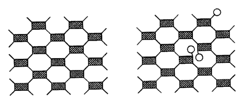
[0008] FIG. 1 illustrates the differences between typical SOF and a
capped SOF. Left hand side: representation of a typical SOF network; right
hand
side: representation of capped SOF illustrating interruptions in the network
and
covalently linked capping group (circle).
[0009] FIG. 2 represents a simplified side view of an exemplary
photoreceptor that incorporates a SOF of the present disclosure.
[0010] FIG. 3 represents a simplified side view of a second exemplary
photoreceptor that incorporates a SOF of the present disclosure.
- 2a -
CA 02746926 2011-07-21
[0011] FIG. 4 represents a simplified side view of a third exemplary
photoreceptor that incorporates a SOF of the present disclosure.
[0012] FIG. 5 represents a simplified side view of a first exemplary thin
film
transistor that incorporates a SOF of the present disclosure.
[0013] FIG. 6 is a graphic representation that compares the Fourier
transform
infrared spectral of the products of control experiments mixtures, wherein
only
N4,N4,N4',N4'-tetrakis(4-(methoxymethyl)phenyl)bipheny1-4,4'-diamine is added
to
the liquid reaction mixture (top), wherein only benzene-1,4-dimethanol is
added to the
liquid reaction mixture (middle), and wherein the necessary components needed
to
form a patterned Type 2 SOF are included into the liquid reaction mixture
(bottom).
[0014] FIG. 7 is a graphic representation of a photo-induced discharge
curve
(PIDC) illustrating the photoconductivity of a Type 2 structured organic film
overcoat
layer.
[0015] FIG. 8 is a graphic representation of TGA curves for capped SOFs
versus a non-capped SOF.
[0016] FIG. 9 is a graphic representation of various stress-strain curves
for
capped SOFs versus a non-capped SOF.
[0017] FIG. 10 is a graphic representation of a photo-induced discharge
curve
(PIDC) illustrating the photoconductivity of a various overcoat layers.
[0018] FIG. 11 is a graphic representation of cycling data that was
acquired
for various overcoat layers.
[0019] Unless otherwise noted, the same reference numeral in different
Figures refers to the same or similar feature.
DETAILED DESCRIPTION
[0020] "Structured organic film" (SOF) refers to a COF that is a film at
a
macroscopic level. The SOFs of the present disclosure have a capping unit or
group
added into the SOF formulation, which (after film formation), ultimately bonds
to the
SOF.
- 3 -
CA 02746926 2011-07-21
=
[0021] In this specification and the claims that follow, singular forms
such as
"a," "an," and "the" include plural forms unless the content clearly dictates
otherwise.
[0022] The term "SOF" generally refers to a covalent organic framework
(COF) that is a film at a macroscopic level. The phrase "macroscopic level"
refers,
for example, to the naked eye view of the present SOFs. Although COFs are a
network at the "microscopic level" or "molecular level" (requiring use of
powerful
magnifying equipment or as assessed using scattering methods), the present SOF
is
fundamentally different at the "macroscopic level" because the film is for
instance
orders of magnitude larger in coverage than a microscopic level COF network.
SOFs
described herein have macroscopic morphologies much different than typical
COFs
previously synthesized.
[0023] Additionally, when a capping unit is introduced into the SOF, the
SOF
framework is locally 'interrupted' where the capping units are present. These
SOF
compositions are `covalently doped' because a foreign molecule is bonded to
the SOF
framework when capping units are present. Capped SOF compositions may alter
the
properties of SOFs without changing constituent building blocks. For example,
the
mechanical and physical properties of the capped SOF where the SOF framework
is
interrupted may differ from that of an uncapped SOF.
[0024] The SOFs of the present disclosure are at the macroscopic level
substantially pinhole-free SOFs or pinhole-free SOFs having continuous
covalent
organic frameworks that can extend over larger length scales such as for
instance
much greater than a millimeter to lengths such as a meter and, in theory, as
much as
hundreds of meters. It will also be appreciated that SOFs tend to have large
aspect
ratios where typically two dimensions of a SOF will be much larger than the
third.
SOFs have markedly fewer macroscopic edges and disconnected external surfaces
than a collection of COF particles.
[0025] In embodiments, a "substantially pinhole-free SOF" or "pinhole-
free
SOF" may be formed from a reaction mixture deposited on the surface of an
underlying substrate. The term "substantially pinhole-free SOF" refers, for
example,
to an SOF that may or may not be removed from the underlying substrate on
which it
- 4 -
CA 02746926 2011-07-21
was formed and contains substantially no pinholes, pores or gaps greater than
the
distance between the cores of two adjacent segments per square cm; such as,
for
example, less than 10 pinholes, pores or gaps greater than about 250
nanometers in
diameter per cm2, or less than 5 pinholes, pores or gaps greater than about
100
nanometers in diameter per cm2. The term "pinhole-free SOF" refers, for
example, to
an SOF that may or may not be removed from the underlying substrate on which
it
was formed and contains no pinholes, pores or gaps greater than the distance
between
the cores of two adjacent segments per micron2, such as no pinholes, pores or
gaps
greater than about 500 Angstroms in diameter per micron2, or no pinholes,
pores or
gaps greater than about 250 Angstroms in diameter per micron2, or no pinholes,
pores
or gaps greater than about 100 Angstroms in diameter per micron2.
[0026] In embodiments, the SOF comprises at least one atom of an element
that is not carbon, such at least one atom selected from the group consisting
of
hydrogen, oxygen, nitrogen, silicon, phosphorous, selenium, fluorine, boron,
and
sulfur. In further embodiments, the SOF is a boroxine-, borazine-,
borosilicate-, and
boronate ester-free SOF.
[0027] Molecular Building Block
[0028] The SOFs of the present disclosure comprise molecular building
blocks having a segment (S) and functional groups (Fg). Molecular building
blocks
require at least two functional groups (x 2) and may comprise a single type or
two
or more types of functional groups. Functional groups are the reactive
chemical
moieties of molecular building blocks that participate in a chemical reaction
to link
together segments during the SOF forming process. A segment is the portion of
the
molecular building block that supports functional groups and comprises all
atoms that
are not associated with functional groups. Further, the composition of a
molecular
building block segment remains unchanged after SOF formation.
[0029] Functional Group
[0030] Functional groups are the reactive chemical moieties of molecular
building blocks that may participate in a chemical reaction to link together
segments
during the SOF forming process. Functional groups may be composed of a single
- 5 -
CA 02746926 2011-07-21
_ = ,
atom, or functional groups may be composed of more than one atom. The atomic
compositions of functional groups are those compositions normally associated
with
reactive moieties in chemical compounds. Non-limiting examples of functional
groups include halogens, alcohols, ethers, ketones, carboxylic acids, esters,
carbonates, amines, amides, imines, ureas, aldehydes, isocyanates, tosylates,
alkenes,
alkynes and the like.
[0031] Molecular building blocks contain a plurality of
chemical moieties, but
only a subset of these chemical moieties are intended to be functional groups
during
the SOF forming process. Whether or not a chemical moiety is considered a
functional group depends on the reaction conditions selected for the SOF
forming
process. Functional groups (Fg) denote a chemical moiety that is a reactive
moiety,
that is, a functional group during the SOF forming process.
[0032] In the SOF forming process the composition of a
functional group will
be altered through the loss of atoms, the gain of atoms, or both the loss and
the gain of
atoms; or, the functional group may be lost altogether. In the SOF, atoms
previously
associated with functional groups become associated with linker groups, which
are the
chemical moieties that join together segments. Functional groups have
characteristic
chemistries and those of ordinary skill in the art can generally recognize in
the present
molecular building blocks the atom(s) that constitute functional group(s). It
should be
noted that an atom or grouping of atoms that are identified as part of the
molecular
building block functional group may be preserved in the linker group of the
SOF.
Linker groups are described below.
[0033] Capping Unit
[00341 Capping units of the present disclosure are molecules
that 'interrupt'
the regular network of covalently bonded building blocks normally present in
an SOF.
The differences between a SOF and a capped SOF are illustrated in Figure 1.
Capped
SOF compositions are tunable materials whose properties can be varied through
the
type and amount of capping unit introduced. Capping units may comprise a
single
type or two or more types of functional groups and/or chemical moieties.
- 6 -
CA 02746926 2013-02-20
"
100351 In embodiments, the capping units have a structure that is
unrelated to
the structure of any of the molecular building blocks that are added into the
SOF
formulation, which (after film formation) ultimately becomes the SOF.
[0036] In embodiments, the capping units have a structure that
substantially
corresponds to the structure of one of the molecular building blocks (such as
the
molecular building blocks for SOFs that are detailed in U.S. Patent
Application Serial
Nos. 12/716,524; 12/716,449; 12/716,706; 12/716,324; 12/716,686; 12/716,571,
and
12/815,688) that is added to the SOF formulation, but one or more of the
functional
groups present on the building block is either missing or has been replaced
with a
different chemical moiety or functional group that will not participate in a
chemical
reaction (with the functional group(s) of the building blocks that are
initially present)
to link together segments during the SOF tot ming process.
[0037] For example, for a molecular building block, such as
tris-(4-hydroxymethyl)triphenylamine:
HO
1401 OH
OH
among the many possible capping units that may be used, suitable capping units
may,
for example, include:
=1401 OH
=1101 c)
OH
and
A capping group having a structure unrelated to the molecular building block
may be,
- 7 -
CA 02746926 2011-07-21
for example, an alkyl moiety (for example, a branched or unbranched saturated
hydrocarbon group, derived from an alkane and having the general formula
CnH2n+1,
in which n is a number of 1 or more) in which one of the hydrogen atoms has
been
replaced by an -OH group. In such a formulation, a reaction between the
capping unit
and the molecular building block, for example, an acid catalyzed reaction
between the
alcohol (-OH) groups, would link the capping unit and the molecular building
blocks
together through the formation of (linking) ether groups.
[0038] In embodiments, the capping unit molecules may be mono-
functionalized. For example, in embodiments, the capping units may comprise
only a
single suitable or complementary functional group (as described above) that
participates in a chemical reaction to link together segments during the SOF
forming
process and thus cannot bridge any further adjacent molecular building blocks
(until a
building block with a suitable or complementary functional group is added,
such as
when an additional SOF is formed on top of a capped SOF base layer and a
multilayer
SOF is formed).
[0039] When such capping units are introduced into the SOF coating
formulation, upon curing, interruptions in the SOF framework are introduced.
Interruptions in the SOF framework are therefore sites where the single
suitable or
complementary functional group of the capping units have reacted with the
molecular
building block and locally terminate (or cap) the extension of the SOF
framework and
interrupt the regular network of covalently bonded building blocks normally
present
in an SOF. The type of capping unit (or structure or the capping unit)
introduced into
the SOF framework may be used to tune the properties of the SOF.
[0040] In embodiments, the capping unit molecules may comprise more than
one chemical moiety or functional group. For example, the SOF coating
formulation,
which (after film formation), ultimately becomes bonded in the SOF may
comprise a
capping unit having at least two or more chemical moieties or functional
groups, such
as 2, 3, 4, 5, 6 or more chemical moieties or functional groups, where only
one of the
functional groups is a suitable or complementary functional group (as
described
above) that participates in a chemical reaction to link together segments
during the
SOF forming process. The various other chemical moieties or functional groups
- 8 -
CA 02746926 2011-07-21
. =
=
present on the molecular building block are chemical moieties or functional
groups
that are not suitable or complementary to participate in the specific chemical
reaction
to link together segments initially present during the SOF forming process and
thus
cannot bridge any further adjacent molecular building blocks. However, after
the
SOF is formed such chemical moieties and/or functional groups may be available
for
further reaction (similar to dangling functional groups, as discussed below)
with
additional components and thus allow for the further refining and tuning of
the
various properties of the formed SOF, or chemically attaching various other
SOF
layers in the formation of multilayer SOFs.
[0041] In embodiments, the molecular building blocks may have x
functional
groups (where x is three or more) and the capping unit molecules may comprise
a
capping unit molecule having x-1 functional groups that are suitable or
complementary functional group (as described above) and participate in a
chemical
reaction to link together segments during the SOF forming process. For
example, x
would be three for tris-(4-hydroxymethyl)triphenylamine (above), and x would
be
four for the building block illustrated below, N,N,M,I\T'-tetrakis-[(4-
hydroxymethyl)phenyn-biphenyl-4,4'-diamine:
HO OH
N * N
HO OH
[0042] A capping unit molecule having x-1 functional groups
that are suitable
or complementary functional groups (as described above) and participate in a
chemical reaction to link together segments during the SOF forming process
would
have 2 functional groups (for a molecular building block such as
tris-(4-hydroxymethyl)triphenylamine), and 3 functional groups (for
N,N,I=11,1\Y-
tetrakis-[(4-hydroxymethyl)phenyThbiphenyl-4,4'-diamine) that are suitable or
complementary functional group (as described above) and participate in a
chemical
reaction to link together segments during the SOF forming process. The other
- 9 -
CA 02746926 2011-07-21
functional group present may be a chemical moiety or a functional group that
is not
suitable or complementary to participate in the specific chemical reaction to
link
together segments during the SOF forming process and thus cannot bridge any
further
adjacent molecular building blocks. However, after the SOF is formed such
functional groups may be available for further reaction with additional
components
and thus allowing for the further refining and tuning of the various
properties of the
formed SOF.
[0043] In embodiments, the capping unit may comprise a mixture of capping
units, such as any combination of a first capping unit, a second capping unit,
a third
capping unit, a fourth capping unit, etc., where the structure of the capping
unit varies.
In embodiments, the structure of a capping unit or a combination of multiple
capping
units may be selected to either enhance or attenuate the chemical and physical
properties of SOF; or the identity of the chemical moieties or functional
group(s) on
that are not suitable or complementary to participate in the chemical reaction
to link
together segments during the SOF forming process may be varied to form a
mixture
of capping units. Thus, the type of capping unit introduced into the SOF
framework
may be selected to introduce or tune a desired property of SOF.
[0044] In embodiments, a SOF contains segments, which are not located at
the
edges of the SOF, that are connected by linkers to at least three other
segments and/or
capping groups. For example, in embodiments the SOF comprises at least one
symmetrical building block selected from the group consisting of ideal
triangular
building blocks, distorted triangular building blocks, ideal tetrahedral
building blocks,
distorted tetrahedral building blocks, ideal square building blocks, and
distorted
square building blocks. In embodiments, Type 2 and 3 SOF contains at least one
segment type, which are not located at the edges of the SOF, that are
connected by
linkers to at least three other segments and/or capping groups. For example,
in
embodiments the SOF comprises at least one symmetrical building block selected
from the group consisting of ideal triangular building blocks, distorted
triangular
building blocks, ideal tetrahedral building blocks, distorted tetrahedral
building
blocks, ideal square building blocks, and distorted square building blocks.
- 10 -
CA 02746926 2011-07-21
[0045] In embodiments, the SOF comprises a plurality of segments, where
all
segments have an identical structure, and a plurality of linkers, which may or
may not
have an identical structure, wherein the segments that are not at the edges of
the SOF
are connected by linkers to at least three other segments and/or capping
groups. In
embodiments, the SOF comprises a plurality of segments where the plurality of
segments comprises at least a first and a second segment that are different in
structure,
and the first segment is connected by linkers to at least three other segments
and/or
capping groups when it is not at the edge of the SOF.
[0046] In embodiments, the SOF comprises a plurality of linkers including
at
least a first and a second linker that are different in structure, and the
plurality of
segments either comprises at least a first and a second segment that are
different in
structure, where the first segment, when not at the edge of the SOF, is
connected to at
least three other segments and/or capping groups, wherein at least one of the
connections is via the first linker, and at least one of the connections is
via the second
linker; or comprises segments that all have an identical structure, and the
segments
that are not at the edges of the SOF are connected by linkers to at least
three other
segments and/or capping groups, wherein at least one of the connections is via
the
first linker, and at least one of the connections is via the second linker.
[0047] Segment
[0048] A segment is the portion of the molecular building block that
supports
functional groups and comprises all atoms that are not associated with
functional
groups. Further, the composition of a molecular building block segment remains
unchanged after SOF formation. In embodiments, the SOF may contain a first
segment having a structure the same as or different from a second segment. In
other
embodiments, the structures of the first and/or second segments may be the
same as or
different from a third segment, forth segment, fifth segment, etc. A segment
is also
the portion of the molecular building block that can provide an inclined
property.
Inclined properties are described later in the embodiments.
[0049] In specific embodiments, the segment of the SOF comprises at least
one atom of an element that is not carbon, such at least one atom selected
from the
- 11 -
CA 02746926 2013-02-20
group consisting of hydrogen, oxygen, nitrogen, silicon, phosphorous,
selenium,
fluorine, boron, and sulfur.
[0050] A description of various exemplary molecular building blocks,
linkers,
SOF types, strategies to synthesize a specific SOF type with exemplary
chemical
structures, building blocks whose symmetrical elements are outlined, and
classes of
exemplary molecular entities and examples of members of each class that may
serve
as molecular building blocks for SOFs are detailed in U.S. Patent Application
Serial
Nos. 12/716,524; 12/716,449; 12/716,706; 12/716,324; 12/716,686; and
12/716,571,
entitled "Structured Organic Films," "Structured Organic Films Having an Added
Functionality," "Mixed Solvent Process for Preparing Structured Organic
Films,"
"Composite Structured Organic Films," "Process For Preparing Structured
Organic
Films (SOFs) Via a Pre-SOF," "Electronic Devices Comprising Structured Organic
Films".
[0051] Linker
100521 A linker is a chemical moiety that emerges in a SOF upon chemical
reaction between functional groups present on the molecular building blocks
and/or
capping unit.
[0053] A linker may comprise a covalent bond, a single atom, or a group
of
covalently bonded atoms. The former is defined as a covalent bond linker and
may
be, for example, a single covalent bond or a double covalent bond and emerges
when
functional groups on all partnered building blocks are lost entirely. The
latter linker
type is defined as a chemical moiety linker and may comprise one or more atoms
bonded together by single covalent bonds, double covalent bonds, or
combinations of
the two. Atoms contained in linking groups originate from atoms present in
functional groups on molecular building blocks prior to the SOF foiming
process.
Chemical moiety linkers may be well-known chemical groups such as, for
example,
esters, ketones, amides, imines, ethers, urethanes, carbonates, and the like,
or
derivatives thereof
- 12-
CA 02746926 2011-07-21
[0054] For example, when two hydroxyl (-OH) functional groups are used to
connect segments in a SOF via an oxygen atom, the linker would be the oxygen
atom,
which may also be described as an ether linker. In embodiments, the SOF may
contain a first linker having a structure the same as or different from a
second linker.
In other embodiments, the structures of the first and/or second linkers may be
the
same as or different from a third linker, etc.
[0055] A capping unit may be bonded in the SOF in any desired amount as
long as the general SOF framework is sufficiently maintained. For example, in
embodiments, a capping unit may be bonded to at least 0.1% of all linkers, but
not
more than about 40% of all linkers present in an SOF, such as from about 0.5%
to
about 30%, or from about 2% to about 20%. In embodiments, substantially all
segments may be bound to at least one capping unit, where the term
"substantially all"
refers, for example, to more than about 95%, such as more than about 99% of
the
segments of the SOF. In the event capping units bond to more than 50% of the
available functional groups on the molecular building blocks (from which the
linkers
emerge), oligomers, linear polymers, and molecular building blocks that are
fully
capped with capping units may predominately form instead of a SOF.
[0056] In specific embodiments, the linker comprises at least one atom of
an
element that is not carbon, such at least one atom selected from the group
consisting
of hydrogen, oxygen, nitrogen, silicon, phosphorous, selenium, fluorine,
boron, and
sulfur.
[0057] Metrical Parameters of SOFs
[0058] SOFs have any suitable aspect ratio. In embodiments, SOFs have
aspect ratios for instance greater than about 30:1 or greater than about 50:1,
or greater
than about 70:1, or greater than about 100:1, such as about 1000:1. The aspect
ratio
of a SOF is defined as the ratio of its average width or diameter (that is,
the dimension
next largest to its thickness) to its average thickness (that is, its shortest
dimension).
The term 'aspect ratio,' as used here, is not bound by theory. The longest
dimension
of a SOF is its length and it is not considered in the calculation of SOF
aspect ratio.
- 13 -
CA 02746926 2011-07-21
. .
[00591 Generally, SOFs have widths and lengths, or diameters
greater than
about 500 micrometers, such as about 10 mm, or 30 mm. The SOFs have the
following illustrative thicknesses: about 10 Angstroms to about 250 Angstroms,
such
as about 20 Angstroms to about 200 Angstroms, for a mono-segment thick layer
and
about 20 nm to about 5 mm, about 50 nm to about 10 mm for a multi-segment
thick
layer.
[0060] SOF dimensions may be measured using a variety of tools
and
methods. For a dimension about 1 micrometer or less, scanning electron
microscopy
is the preferred method. For a dimension about 1 micrometer or greater, a
micrometer
(or ruler) is the preferred method.
[0061] Multilayer SOFs
[0062] A SOF may comprise a single layer or a plurality of
layers (that is,
two, three or more layers). SOFs that are comprised of a plurality of layers
may be
physically joined (e.g., dipole and hydrogen bond) or chemically joined.
Physically
attached layers are characterized by weaker interlayer interactions or
adhesion;
therefore physically attached layers may be susceptible to delamination from
each
other. Chemically attached layers are expected to have chemical bonds (e.g.,
covalent
or ionic bonds) or have numerous physical or intermolecular (supramolecular)
entanglements that strongly link adjacent layers.
[0063] Therefore, delamination of chemically attached layers is
much more
difficult. Chemical attachments between layers may be detected using
spectroscopic
methods such as focusing infrared or Raman spectroscopy, or with other methods
having spatial resolution that can detect chemical species precisely at
interfaces. In
cases where chemical attachments between layers are different chemical species
than
those within the layers themselves it is possible to detect these attachments
with
sensitive bulk analyses such as solid-state nuclear magnetic resonance
spectroscopy or
by using other bulk analytical methods.
[0064] In the embodiments, the SOF may be a single layer (mono-
segment
thick or multi-segment thick) or multiple layers (each layer being mono-
segment thick
or multi-segment thick). "Thickness" refers, for example, to the smallest
dimension
- 14 -
CA 02746926 2011-07-21
, . = .
of the film. As discussed above, in a SOF, segments are molecular units that
are
covalently bonded through linkers to generate the molecular framework of the
film.
The thickness of the film may also be defined in terms of the number of
segments that
is counted along that axis of the film when viewing the cross-section of the
film. A
"monolayer" SOF is the simplest case and refers, for example, to where a film
is one
segment thick. A SOF where two or more segments exist along this axis is
referred to
as a "multi-segment" thick SOF.
[0065] An exemplary method for preparing physically attached
multilayer
SOFs includes: (1) forming a base SOF layer that may be cured by a first
curing
cycle, and (2) forming upon the base layer a second reactive wet layer
followed by a
second curing cycle and, if desired, repeating the second step to form a third
layer, a
forth layer and so on. The physically stacked multilayer SOFs may have
thicknesses
greater than about 20 Angstroms such as, for example, the following
illustrative
thicknesses: about 20 Angstroms to about 10 cm, such as about 1 nm to about 10
mm, or about 0.1 mm Angstroms to about 5 mm. In principle there is no limit
with
this process to the number of layers that may be physically stacked.
[0066] In embodiments, a multilayer SOF is formed by a method
for preparing
chemically attached multilayer SOFs by: (1) forming a base SOF layer having
functional groups present on the surface (or dangling functional groups) from
a first
reactive wet layer, and (2) forming upon the base layer a second SOF layer
from a
second reactive wet layer that comprises molecular building blocks with
functional
groups capable of reacting with the dangling functional groups on the surface
of the
base SOF layer. In further embodiments, a capped SOF may serve as the base
layer in
which the functional groups present that were not suitable or complementary to
participate in the specific chemical reaction to link together segments during
the base
layer SOF forming process may be available for reacting with the molecular
building
blocks of the second layer to form a chemically bonded multilayer SOF. If
desired,
the formulation used to form the second SOF layer should comprise molecular
building blocks with functional groups capable of reacting with the functional
groups
from the base layer as well as additional functional groups that will allow
for a third
layer to be chemically attached to the second layer. The chemically stacked
- 15 -
CA 02746926 2011-07-21
=
multilayer SOFs may have thicknesses greater than about 20 Angstroms such as,
for
example, the following illustrative thicknesses: about 20 Angstroms to about
10 cm,
such as about 1 nm to about 10 mm, or about 0.1 mm Angstroms to about 5 mm. In
principle there is no limit with this process to the number of layers that may
be
chemically stacked.
[0067] In embodiments, the method for preparing chemically
attached
multilayer SOFs comprises promoting chemical attachment of a second SOF onto
an
existing SOF (base layer) by using a small excess of one molecular building
block
(when more than one molecular building block is present) during the process
used to
form the SOF (base layer) whereby the functional groups present on this
molecular
building block will be present on the base layer surface. The surface of base
layer
may be treated with an agent to enhance the reactivity of the functional
groups or to
create an increased number of functional groups.
[0068] In an embodiment the dangling functional groups or
chemical moieties
present on the surface of an SOF or capped SOF may be altered to increase the
propensity for covalent attachment (or, alternatively, to disfavor covalent
attachment)
of particular classes of molecules or individual molecules, such as SOFs, to a
base
layer or any additional substrate or SOF layer. For example, the surface of a
base
layer, such as an SOF layer, which may contain reactive dangling functional
groups,
may be rendered pacified through surface treatment with a capping chemical
group.
For example, a SOF layer having dangling hydroxyl alcohol groups may be
pacified
by treatment with trimethylsiylchloride thereby capping hydroxyl groups as
stable
trimethylsilylethers. Alternatively, the surface of base layer may be treated
with a
non-chemically bonding agent, such as a wax, to block reaction with dangling
functional groups from subsequent layers.
[0069] Molecular Building Block Symmetry
[0070] Molecular building block symmetry relates to the
positioning of
functional groups (Fgs) around the periphery of the molecular building block
segments. Without being bound by chemical or mathematical theory, a symmetric
molecular building block is one where positioning of Fgs may be associated
with the
- 16 -
CA 02746926 2011-07-21
,
. .
ends of a rod, vertexes of a regular geometric shape, or the vertexes of a
distorted rod
or distorted geometric shape. For example, the most symmetric option for
molecular
building blocks containing four Fgs are those whose Fgs overlay with the
corners of a
square or the apexes of a tetrahedron.
[0071] Use of symmetrical building blocks is practiced in
embodiments of the
present disclosure for two reasons: (1) the patterning of molecular building
blocks
may be better anticipated because the linking of regular shapes is a better
understood
process in reticular chemistry, and (2) the complete reaction between
molecular
building blocks is facilitated because for less symmetric building blocks
errant
conformations/orientations may be adopted which can possibly initiate numerous
linking defects within SOFs.
[0072] In embodiments, a Type 1 SOF contains segments, which are
not
located at the edges of the SOF, that are connected by linkers to at least
three other
segments. For example, in embodiments the SOF comprises at least one
symmetrical
building block selected from the group consisting of ideal triangular building
blocks,
distorted triangular building blocks, ideal tetrahedral building blocks,
distorted
tetrahedral building blocks, ideal square building blocks, and distorted
square building
blocks. In embodiments, Type 2 and 3 SOF contains at least one segment type,
which
are not located at the edges of the SOF, that are connected by linkers to at
least three
other segments. For example, in embodiments the SOF comprises at least one
symmetrical building block selected from the group consisting of ideal
triangular
building blocks, distorted triangular building blocks, ideal tetrahedral
building blocks,
distorted tetrahedral building blocks, ideal square building blocks, and
distorted
square building blocks.
[0073] Practice of Linking Chemistry
[00741 In embodiments linking chemistry may occur wherein the
reaction
between functional groups produces a volatile byproduct that may be largely
evaporated or expunged from the SOF during or after the film forming process
or
wherein no byproduct is formed. Linking chemistry may be selected to achieve a
SOF for applications where the presence of linking chemistry byproducts is not
- 17 -
CA 02746926 2011-07-21
. .
. .
desired. Linking chemistry reactions may include, for example, condensation,
addition/elimination, and addition reactions, such as, for example, those that
produce
esters, imines, ethers, carbonates, urethanes, amides, acetals, and silyl
ethers.
[0075] In embodiments the linking chemistry via a reaction
between function
groups producing a non-volatile byproduct that largely remains incorporated
within
the SOF after the film forming process. Linking chemistry in embodiments may
be
selected to achieve a SOF for applications where the presence of linking
chemistry
byproducts does not impact the properties or for applications where the
presence of
linking chemistry byproducts may alter the properties of a SOF (such as, for
example,
the electroactive, hydrophobic or hydrophilic nature of the SOF). Linking
chemistry
reactions may include, for example, substitution, metathesis, and metal
catalyzed
coupling reactions, such as those that produce carbon-carbon bonds.
[0076] For all linking chemistry the ability to control the rate
and extent of
reaction between building blocks via the chemistry between building block
functional
groups is an important aspect of the present disclosure. Reasons for
controlling the
rate and extent of reaction may include adapting the film forming process for
different
coating methods and tuning the microscopic arrangement of building blocks to
achieve a periodic SOF, as defined in earlier embodiments.
[0077] Innate Properties of COFs
[0078] COFs have innate properties such as high thermal
stability (typically
higher than 400 C under atmospheric conditions); poor solubility in organic
solvents
(chemical stability), and porosity (capable of reversible guest uptake). In
embodiments, SOFs may also possess these innate properties.
[0079] Added Functionality of SOFs
[0080] Added functionality denotes a property that is not
inherent to
conventional COFs and may occur by the selection of molecular building blocks
wherein the molecular compositions provide the added functionality in the
resultant
SOF. Added functionality may arise upon assembly of molecular building blocks
and/or capping units having an "inclined property" for that added
functionality.
Added functionality may also arise upon assembly of molecular building blocks
- 18 -
CA 02746926 2011-07-21
. .
. .
having no "inclined property" for that added functionality but the resulting
SOF has
the added functionality as a consequence of linking segments (S) and linkers
into a
SOF. In embodiments, added functionality may also arise upon the addition and
assembly of molecular building blocks and capping units having no "inclined
property" for that added functionality but the resulting SOF has the added
functionality as a consequence of linking segments, linkers, and capping units
into a
SOF. Furthermore, emergence of added functionality may arise from the combined
effect of using molecular building blocks bearing an "inclined property" for
that
added functionality whose inclined property is modified or enhanced upon
linking
together the segments and linkers into a SOF.
[0081] An Inclined Property of a Molecular Building Block
[0082] The term "inclined property" of a molecular building
block refers, for
example, to a property known to exist for certain molecular compositions or a
property that is reasonably identifiable by a person skilled in art upon
inspection of
the molecular composition of a segment. As used herein, the terms "inclined
property" and "added functionality" refer to the same general property (e.g.,
hydrophobic, electroactive, etc.) but "inclined property" is used in the
context of the
molecular building block and "added functionality" is used in the context of
the SOF.
[0083] The hydrophobic (superhydrophobic), hydrophilic,
lipophobic
(superlipophobic), lipophilic, photochromic and/or electroactive (conductor,
semiconductor, charge transport material) nature of an SOF are some examples
of the
properties that may represent an "added functionality" of an SOF. These and
other
added functionalities may arise from the inclined properties of the molecular
building
blocks or may arise from building blocks that do not have the respective added
functionality that is observed in the SOF.
[0084] The term hydrophobic (superhydrophobic) refers, for
example, to the
property of repelling water, or other polar species such as methanol, it also
means an
inability to absorb water and/or to swell as a result. Furthermore,
hydrophobic
implies an inability to form strong hydrogen bonds to water or other hydrogen
bonding species. Hydrophobic materials are typically characterized by having
water
- 19 -
CA 02746926 2011-07-21
contact angles greater than 900 and superhydrophobic materials have water
contact
angles greater than 1500 as measured using a contact angle goniometer or
related
device.
[0085] The term hydrophilic refers, for example, to the property of
attracting,
adsorbing, or absorbing water or other polar species, or a surface that is
easily wetted
by such species. Hydrophilic materials are typically characterized by having
less than
200 water contact angle as measured using a contact angle goniometer or
related
device. Hydrophilicity may also be characterized by swelling of a material by
water
or other polar species, or a material that can diffuse or transport water, or
other polar
species, through itself. Hydrophilicity, is further characterized by being
able to form
strong or numerous hydrogen bonds to water or other hydrogen bonding species.
[0086] The term lipophobic (oleophobic) refers, for example, to the
property
of repelling oil or other non-polar species such as alkanes, fats, and waxes.
Lipophobic materials are typically characterized by having oil contact angles
greater
than 90 as measured using a contact angle goniometer or related device.
[0087] The term lipophilic (oleophilic) refers, for example, to the
property
attracting oil or other non-polar species such as alkanes, fats, and waxes or
a surface
that is easily wetted by such species. Lipophilic materials are typically
characterized
by having a low to nil oil contact angle as measured using, for example, a
contact
angle goniometer. Lipophilicity can also be characterized by swelling of a
material
by hexane or other non-polar liquids.
[0088] The term photochromic refers, for example, to the ability to
demonstrate reversible color changes when exposed to electromagnetic
radiation.
SOF compositions containing photochromic molecules may be prepared and
demonstrate reversible color changes when exposed to electromagnetic
radiation.
These SOFs may have the added functionality of photochromism. The robustness
of
photochromic SOFs may enable their use in many applications, such as
photochromic
SOFs for erasable paper, and light responsive films for window tinting/shading
and
eye wear. SOF compositions may contain any suitable photochromic molecule,
such
as a difunctional photochromic molecules as SOF molecular building blocks
- 20 -
CA 02746926 2011-07-21
(chemically bound into SOF structure), a monofunctional photochromic molecules
as
SOF capping units (chemically bound into SOF structure, or unfunctionalized
photochromic molecules in an SOF composite (not chemically bound into SOF
structure). Photochromic SOFs may change color upon exposure to selected
wavelengths of light and the color change may be reversible.
[0089] SOF compositions containing photochromic molecules that chemically
bond to the SOF structure are exceptionally chemically and mechanically robust
photochromic materials. Such photochromic SOF materials demonstrate many
superior properties, such as high number of reversible color change processes,
to
available polymeric alternatives.
[0090] The term electroactive refers, for example, to the property to
transport
electrical charge (electrons and/or holes). Electroactive materials include
conductors,
semiconductors, and charge transport materials. Conductors are defined as
materials
that readily transport electrical charge in the presence of a potential
difference.
Semiconductors are defined as materials do not inherently conduct charge but
may
become conductive in the presence of a potential difference and an applied
stimuli,
such as, for example, an electric field, electromagnetic radiation, heat, and
the like.
Charge transport materials are defined as materials that can transport charge
when
charge is injected from another material such as, for example, a dye, pigment,
or
metal in the presence of a potential difference.
[0091] Conductors may be further defined as materials that give a signal
using
a potentiometer from about 0.1 to about 107 S/cm.
[0092] Semiconductors may be further defined as materials that give a
signal
using a potentiometer from about le to about 104 S/cm in the presence of
applied
stimuli such as, for example an electric field, electromagnetic radiation,
heat, and the
like. Alternatively, semiconductors may be defined as materials having
electron
and/or hole mobility measured using time-of-flight techniques in the range of
10-' to
about 106 cm2V-1s-1 when exposed to applied stimuli such as, for example an
electric
field, electromagnetic radiation, heat, and the like.
- 21 -
CA 02746926 2011-07-21
[0093] Charge transport materials may be further defined as materials
that
have electron and/or hole mobility measured using time-of-flight techniques in
the
range of 10-10 to about 106 cm2V-1s1. It should be noted that under some
circumstances charge transport materials may be also classified as
semiconductors.
[0094] SOFs with hydrophobic added functionality may be prepared by using
molecular building blocks with inclined hydrophobic properties and/or have a
rough,
textured, or porous surface on the sub-micron to micron scale. A paper
describing
materials having a rough, textured, or porous surface on the sub-micron to
micron
scale being hydrophobic was authored by Cassie and Baxter (Cassie, A. B. D.;
Baxter,
S. Trans. Faraday Soc., 1944, 40, 546).
[0095] Molecular building blocks comprising or bearing highly-fluorinated
segments have inclined hydrophobic properties and may lead to SOFs with
hydrophobic added functionality. Highly-fluorinated segments are defined as
the
number of fluorine atoms present on the segment(s) divided by the number of
hydrogen atoms present on the segment(s) being greater than one. Fluorinated
segments, which are not highly-fluorinated segments may also lead to SOFs with
hydrophobic added functionality.
[0096] The above-mentioned fluorinated segments may include, for example,
tetrafluorohydroquinone, perfluoroadipic acid hydrate, 4,4'-
(hexafluoroisopropylidene)diphthalic anhydride, 4,4'-
(hexafluoroisopropylidene)diphenol, and the like.
[0097] SOFs having a rough, textured, or porous surface on the sub-micron
to
micron scale may also be hydrophobic. The rough, textured, or porous SOF
surface
can result from dangling functional groups present on the film surface or from
the
structure of the SOF. The type of pattern and degree of patterning depends on
the
geometry of the molecular building blocks and the linking chemistry
efficiency. The
feature size that leads to surface roughness or texture is from about 100 nm
to about
pm, such as from about 500 nm to about 5 wn.
- 22 -
CA 02746926 2011-07-21
[0098] SOFs with hydrophilic added functionality may be prepared by using
molecular building blocks with inclined hydrophilic properties and/or
comprising
polar linking groups.
[0099] Molecular building blocks comprising segments bearing polar
substituents have inclined hydrophilic properties and may lead to SOFs with
hydrophilic added functionality. The term polar substituents refers, for
example, to
substituents that can form hydrogen bonds with water and include, for example,
hydroxyl, amino, ammonium, and carbonyl (such as ketone, carboxylic acid,
ester,
amide, carbonate, urea).
[00100] SOFs with electroactive added functionality may be prepared by
using
molecular building blocks with inclined electroactive properties and/or be
electroactive resulting from the assembly of conjugated segments and linkers.
The
following sections describe molecular building blocks with inclined hole
transport
properties, inclined electron transport properties, and inclined semiconductor
properties.
[00101] SOFs with hole transport added functionality may be obtained by
selecting segment cores such as, for example, triarylamines, hydrazones (U.S.
Patent
No. 7,202,002 B2 to Tokarski et al.), and enamines (U.S. Patent No. 7,416,824
B2 to
Kondoh et al.) with the following general structures:
AO\ Ar3 Arl Ar4
1=1¨Ar5 Ni /
C=N¨N/
= µ Ar2 ¨r4 / =
Ar2 Ar4) Arl NA ,
k Ar3
Ar
triarylamine enamines hydrazones
The segment core comprising a triarylamine being represented by the following
general formula:
Arl\ Ar3
11¨Ar5
=
Ar2 \Ar4)k
wherein Arl, Ar2, Ar3, Ar4 and Ar5 each independently represents a substituted
or
unsubstituted aryl group, or Ar5 independently represents a substituted or
- 23 -
CA 02746926 2011-07-21
= :
unsubstituted arylene group, and k represents 0 or 1, wherein at least two of
Arl, Ar2,
Ar3, Ar4 and Ar5 comprises a Fg (previously defined). Ar5 may be further
defined as,
for example, a substituted phenyl ring, substituted/unsubstituted phenylene,
substituted/unsubstituted monovalently linked aromatic rings such as biphenyl,
terphenyl, and the like, or substituted/unsubstituted fused aromatic rings
such as
naphthyl, anthranyl, phenanthryl, and the like.
[00102] Segment cores comprising arylamines with hole transport added
functionality include, for example, aryl amines such as triphenylamine,
N,N,N',N'-
tetraphenyl-(1,11-bipheny1)-4,4'-diamine, N,N'-diphenyl-N,N1-bis(3-
methylpheny1)-
(1,1'-bipheny1)-4,4'-diamine, N,Nr-bis(4-butylpheny1)-N,N'-diphenyljp-
terpheny1]-
4,4"-diamine; hydrazones such as N-phenyl-N-methyl-3-(9-ethyl)carbazyl
hydrazone
and 4-diethyl amino benzaldehyde-1,2-diphenyl hydrazone; and oxadiazoles such
as
2,5-bis(4-N,N'-diethylaminopheny1)-1,2,4-oxadiazole, stilbenes, and the like.
[00103] Molecular building blocks comprising triarylamine core
segments with
inclined hole transport properties may be derived from the list of chemical
structures
including, for example, those listed below:
- 24 -
CA 02746926 2011-07-21
. :
triarylamine cores
Fg¨Q Fg¨Q Fg¨Q
* li Ilk
N * Ck N * * N *
4. Fg
ilk II *
Fg¨Q Fg¨Q Fg¨Q
11
Fg¨Q Fg¨Q F9¨Q
N * N * N II
* *
Fg¨Q Fg¨Q Fg¨Q
Fg¨Q Fg¨Q Fg¨Q
* Me
* *
N * Me
ilk lik * II
Fg¨Q Fg¨Q Fg¨Q
tetraarylbiphenylenediamine (TBD) cores
tetraarylterphenylenediamine (TER) cores
Fg¨Q O¨Fg Fg¨Q Q¨Fg
N * 411 N
* * lik *
Fg¨Q Q¨Fg Fg¨Q Q¨Fg
R
R Q¨Fg Q¨Fg
ilk GI * 41
* A * A
Fg¨Q R Fg¨Q R
[00104] The
segment core comprising a hydrazone being represented by the
following general formula:
- 25 -
CA 02746926 2011-07-21
. =
Arl Ar2
\ t
C=N¨N
Ar3
wherein Arl, Ar2, and Ar3 each independently represents an aryl group
optionally
containing one or more substituents, and R represents a hydrogen atom, an aryl
group,
or an alkyl group optionally containing a substituent; wherein at least two of
Ari, Ar2,
and Ar3 comprises a Fg (previously defined); and a related oxadiazole being
represented by the following general formula:
N¨N
C
Ar = ==
0
wherein Ar and Arl each independently represent an aryl group that comprises a
Fg
(previously defined).
[00105] Molecular building blocks comprising hydrazone and
oxadiazole core
segments with inclined hole transport properties may be derived from the list
of
chemical structures including, for example, those listed below:
- 26 -
CA 02746926 2011-07-21
hydrazone cores
H µ1\1 * Me µN1 *
µFg
Fg
Fg¨Q Fg¨Q
Et2N Et2N
H µN Qk Me µNI * Qµ
Fg
Fg
Fg¨Q Fg¨Q
Et2N Me
*
_NFg
H N *
*
µ Q
* 111 H t\J
Fg
Fg¨Q
Fg¨Q
oxadiazole cores
N¨N
Fg * '0' 110 ,Fg
[00106] The segment core comprising an enamine being represented by the
following general formula:
Arl\ tR
C=C
i \
Ar2 N¨Ar4
Ar3
wherein Ari, Ar2, Ar3, and Ar4 each independently represents an aryl group
that
optionally contains one or more substituents or a heterocyclic group that
optionally
- 27 -
CA 02746926 2011-07-21
=
contains one or more substituents, and R represents a hydrogen atom, an aryl
group,
or an alkyl group optionally containing a substituent; wherein at least two of
Ari, Ar2,
Ar3, and Ar4 comprises a Fg (previously defined).
[00107] Molecular building blocks comprising enamine core
segments with
inclined hole transport properties may be derived from the list of chemical
structures
including, for example, those listed below:
enamine cores
Fg¨Q
Fg¨Q
Ph H
>=7:(
Ph N
Fg N QµFg
Ph/N¨Ph
Fg¨Q Fg¨Q 140
Fg¨Q
Fg
Fg¨Q
Fg¨Q
111
Ph Me
Ph)----=(N * Me Me
µFg
00
NQ
Fg
/to Ph/N¨Ph
Fg¨Q Fg¨Q
Fg¨Q
,
FgQ"
Fg¨Q
Fg¨Q
Ph Ph
Ph)--(N * Q Ph Ph
N
Fg
'ft
Fg
Ph71¨Ph
Fg¨Q Fg ¨Q
Fg¨,0
Fg.-Q
[00108] SOFs with electron transport added functionality may be
obtained by
selecting segment cores comprising, for example, nitrofluorenones, 9-
fluorenylidene
malonitriles, diphenoquinones, and naphthalenetetracarboxylic diimides with
the
following general structures:
- 28 -
CA 02746926 2011-07-21
0 NC CN
Fg1S * N1Q'Fg *
02N Fg, sca,,Fg
Q
nitrofluorenones 94Iuorenylidene malonitriles
0 Ak. 0
Fg
o NQ¨N \WAIL/ N¨Q
Fg
FIg FIg 0 0
dlphenoguinones naphthalenetetracarboxylic diimides
It should be noted that the carbonyl groups of diphenylquinones could also act
as Fgs
in the SOF forming process.
[001091 SOFs with semiconductor added functionality may be obtained by
selecting segment cores such as, for example, acenes,
thiophenes/oligothiophenes/fused thiophenes, perylene bisimides, or
tetrathiofulvalenes, and derivatives thereof with the following general
structures:
H 0 0
S n II II
*op] n R¨N* N¨R
acenes H H 0
perylene bisimides 0
S n
S 1 S >=<
HA) *
H H
oligothiophenes tetrathiofulvalenes
fused thiophenes
[00110] The SOF may be a p-type semiconductor, n-type semiconductor or
ambipolar semiconductor. The SOF semiconductor type depends on the nature of
the
molecular building blocks. Molecular building blocks that possess an electron
donating property such as alkyl, alkoxy, aryl, and amino groups, when present
in the
SOF, may render the SOF a p-type semiconductor. Alternatively, molecular
building
blocks that are electron withdrawing such as cyano, nitro, fluoro, fluorinated
alkyl,
and fluorinated aryl groups may render the SOF into the n-type semiconductor.
- 29 -
CA 02746926 2011-07-21
4
[00M] Molecular building blocks comprising acene core segments with
inclined semiconductor properties may be derived from the list of chemical
structures
including, for example, those listed below:
o'Fg
0040
Fg, .,Fg
Q
Fg Q" (;)
I* II
Fgµcl 000 SOO.
¨Q
µFg
II )1
Fg, F, g
Q Q"
Fg',Q QµFg
10000
Fg,,Q Q
'Fg
[00112] Molecular building blocks comprising
thiophene/oligothiophene/fused
thiophene core segments with inclined semiconductor properties may be derived
from
the list of chemical structures including, for example, those listed below:
,Q S Fg
Fg- 'stir 'Fg
Fg s
Fg--a Q--Fg
Fg, Fg,
Fg/
, s ,Fg
Q / Q R R
/
/ 8 Q
S
Fg S Fg
Q,Fg
'Fg
(or isomer and mixtures)
(or isomer and mixtures) (or isomer
and mixtures)
Q¨Fg
Fg
0
S S S S S S
Fg
Fg¨Q
Fg¨Q Q¨Fg
Fg Fg
S S S 4 S S S
S S S 9 \ s s S
Fg Fg
Q¨Fg Fg¨Q
- 30 -
CA 02746926 2011-07-21
[00113] Examples of molecular building blocks comprising perylene bisimide
core segments with inclined semiconductor properties may be derived from the
chemical structure below:
0
--
Fg)aN 4114101111 N¨ciFg
[00114] Molecular building blocks comprising tetrathiofulvalene core
segments
with inclined semiconductor properties may be derived from the list of
chemical
structures including, for example, those listed below:
= s>=<S
QFg
/LS)==<S-)\
Fg S S
Fg Fg
Fg
>=<S
Fg Q-LS>=:<SS'IC11
/
S S
a
Fg/
µFg
iFg
I ¨0
Fg Fg
al
S S F0
Fg CtS>=<S Qi
/ S S
Fg/ µFg
wherein Ar each independently represents an aryl group that optionally
contains one
or more substituents or a heterocyclic group that optionally contains one or
more
substituents.
[00115] Similarly, the electroactivity of SOFs prepared by these molecular
building blocks will depend on the nature of the segments, nature of the
linkers, and
how the segments are orientated within the SOF. Linkers that favor preferred
orientations of the segment moieties in the SOF are expected to lead to higher
electroactivity.
[00116] Process for Preparing a Capped Structured Organic Film (SOF)
-31-
CA 02746926 2011-07-21
,
. .
[00117] The process for making capped SOFs (which may be referred
to as an
"SOF" below) typically comprises a similar number of activities or steps (set
forth
below) that are used to make a non-capped SOF. The capping unit may be added
during either step a, b or c, depending the desired distribution of the
capping unit in
the resulting SOF. For example, if it is desired that the capping unit
distribution is
substantially uniform over the resulting SOF, the capping unit may be added
during
step a. Alternatively, if, for example, a more heterogeneous distribution of
the capping
unit is desired, adding the capping unit (such as by spraying it on the film
formed
during step b or during the promotion step of step c) may occur during steps b
and c.
[00118] The process for making SOFs typically comprises a number
of
activities or steps (set forth below) that may be performed in any suitable
sequence or
where two or more activities are performed simultaneously or in close
proximity in
time:
A process for preparing a structured organic film comprising:
(a) preparing a liquid-containing reaction mixture comprising a plurality of
molecular
building blocks each comprising a segment and a number of functional groups;
(b) depositing the reaction mixture as a wet film;
(c) promoting a change of the wet film including the molecular building blocks
to a
dry film comprising the SOF comprising a plurality of the segments and a
plurality of
linkers arranged as a covalent organic framework, wherein at a macroscopic
level the
covalent organic framework is a film;
(d) optionally removing the SOF from the coating substrate to obtain a free-
standing
SOF;
(e) optionally processing the free-standing SOF into a roll;
(f) optionally cutting and seaming the SOF into a belt; and
(g) optionally performing the above SOF formation process(es) upon an SOF
(which
was prepared by the above SOF formation process(es)) as a substrate for
subsequent
SOF formation process(es).
-32 -
CA 02746926 2011-07-21
[00119] The above activities or steps may be conducted at atmospheric,
super
atmospheric, or subatmospheric pressure. The term "atmospheric pressure" as
used
herein refers to a pressure of about 760 torr. The term "super atmospheric"
refers to
pressures greater than atmospheric pressure, but less than 20 atm. The term
"subatmospheric pressure" refers to pressures less than atmospheric pressure.
In an
embodiment, the activities or steps may be conducted at or near atmospheric
pressure.
Generally, pressures of from about 0.1 atm to about 2 atm, such as from about
0.5 atm
to about 1.5 atm, or 0.8 atm to about 1.2 atm may be conveniently employed.
[00120] Process Action A: Preparation of the Liquid-Containing Reaction
Mixture
[00121] The reaction mixture comprises a plurality of molecular building
blocks that are dissolved, suspended, or mixed in a liquid. The plurality of
molecular
building blocks may be of one type or two or more types. When one or more of
the
molecular building blocks is a liquid, the use of an additional liquid is
optional.
Catalysts may optionally be added to the reaction mixture to enable SOF
formation or
modify the kinetics of SOF formation during Action C described above.
Additives or
secondary components may optionally be added to the reaction mixture to alter
the
physical properties of the resulting SOF.
[00122] The reaction mixture components (molecular building blocks,
optionally a capping unit, liquid, optionally catalysts, and optionally
additives) are
combined in a vessel. The order of addition of the reaction mixture components
may
vary; however, typically the catalyst is added last. In particular
embodiments, the
molecular building blocks are heated in the liquid in the absence of the
catalyst to aid
the dissolution of the molecular building blocks. The reaction mixture may
also be
mixed, stirred, milled, or the like, to ensure even distribution of the
formulation
components prior to depositing the reaction mixture as a wet film.
[00123] In embodiments, the reaction mixture may be heated prior to being
deposited as a wet film. This may aid the dissolution of one or more of the
molecular
building blocks and/or increase the viscosity of the reaction mixture by the
partial
reaction of the reaction mixture prior to depositing the wet layer. This
approach may
- 33 -
CA 02746926 2011-07-21
:
be used to increase the loading of the molecular building blocks in the
reaction
mixture.
[00124] In particular embodiments, the reaction mixture needs to have a
viscosity that will support the deposited wet layer. Reaction mixture
viscosities range
from about 10 to about 50,000 cps, such as from about 25 to about 25,000 cps
or from
about 50 to about 1000 cps.
[00125] The molecular building block and capping unit loading or
"loading" in
the reaction mixture is defined as the total weight of the molecular building
blocks
and optionally the capping units and catalysts divided by the total weight of
the
reaction mixture. Building block loadings may range from about 3 to 100%, such
as
from about 5 to about 50%, or from about 15 to about 40%. In the case where a
liquid
molecular building block is used as the only liquid component of the reaction
mixture
(i.e. no additional liquid is used), the building block loading would be about
100%.
The capping unit loading may be chosen, so as to achieve the desired loading
of the
capping group. For example, depending on when the capping unit is to be added
to
the reaction mixture, capping unit loadings may range, by weight, from about 3
to
80%, such as from about 5 to about 50%, or from about 15 to about 40% by
weight.
[00126] In embodiments, the theoretical upper limit for capping unit
loading is
the molar amount of capping units that reduces the number of available linking
groups
to 2 per molecular building block in the liquid SOF formulation. In such a
loading,
substantial SOF formation may be effectively inhibited by exhausting (by
reaction
with the respective capping group) the number of available linkable functional
groups
per molecular building block. For example, in such a situation (where the
capping
unit loading is in an amount sufficient to ensure that the molar excess of
available
linking groups is less than 2 per molecular building block in the liquid SOF
formulation), oligomers, linear polymers, and molecular building blocks that
are fully
capped with capping units may predominately form instead of an SOF.
[00127] Liquids used in the reaction mixture may be pure liquids, such
as
solvents, and/or solvent mixtures. Liquids are used to dissolve or suspend the
molecular building blocks and catalyst/modifiers in the reaction mixture.
Liquid
- 34 -
CA 02746926 2011-07-21
selection is generally based on balancing the solubility/dispersion of the
molecular
building blocks and a particular building block loading, the viscosity of the
reaction
mixture, and the boiling point of the liquid, which impacts the promotion of
the wet
layer to the dry SOF. Suitable liquids may have boiling points from about 30
to
about 300 C, such as from about 65 C to about 250 C, or from about 100 C
to
about 180 C.
[00128] Liquids can include molecule classes such as alkanes (hexane,
heptane,
octane, nonane, decane, cyclohexane, cycloheptane, cyclooctane, decalin);
mixed
alkanes (hexanes, heptanes); branched alkanes (isooctane); aromatic compounds
(toluene, a-, m-, p-xylene, mesitylene, nitrobenzene, benzonitrile,
butylbenzene,
aniline); ethers (benzyl ethyl ether, butyl ether, isoamyl ether, propyl
ether); cyclic
ethers (tetrahydrofuran, dioxane), esters (ethyl acetate, butyl acetate, butyl
butyrate,
ethoxyethyl acetate, ethyl propionate, phenyl acetate, methyl benzoate);
ketones
(acetone, methyl ethyl ketone, methyl isobutylketone, diethyl ketone,
chloroacetone,
2-heptanone), cyclic ketones (cyclopentanone, cyclohexanone), amines (10, 2 ,
or 3
amines such as butylamine, diisopropylamine, triethylamine,
diisoproylethylamine;
pyridine); amides (dimethylformamide, N-methylpyrolidinone, /V,N-
dimethylformamide); alcohols (methanol, ethanol, n-, i-propanol, n-, t-
butanol, 1-
methoxy-2-propanol, hexanol, cyclohexanol, 3-pentanol, benzyl alcohol);
nitriles
(acetonitrile, benzonitrile, butyronitrile), halogenated aromatics
(chlorobenzene,
dichlorobenzene, hexafluorobenzene), halogenated alkanes (dichloromethane,
chloroform, dichloroethylene, tetrachloroethane); and water.
[00129] Mixed liquids comprising a first solvent, second solvent, third
solvent,
and so forth may also be used in the reaction mixture. Two or more liquids may
be
used to aid the dissolution/dispersion of the molecular building blocks;
and/or
increase the molecular building block loading; and/or allow a stable wet film
to be
deposited by aiding the wetting of the substrate and deposition instrument;
and/or
modulate the promotion of the wet layer to the dry SOF. In embodiments, the
second
solvent is a solvent whose boiling point or vapor-pressure curve or affinity
for the
molecular building blocks differs from that of the first solvent. In
embodiments, a
first solvent has a boiling point higher than that of the second solvent. In
- 35 -
CA 02746926 2011-07-21
embodiments, the second solvent has a boiling point equal to or less than
about
100 C, such as in the range of from about 30 C to about 100 C, or in the range
of
from about 40 C to about 90 C, or about 50 C to about 80 C.
[00130] In embodiments, the first solvent, or higher boiling point
solvent, has a
boiling point equal to or greater than about 65 C, such as in the range of
from about
80 C to about 300 C, or in the range of from about 100 C to about 250 C, or
about
100 C to about 180 C. The higher boiling point solvent may include, for
example, the
following (the value in parentheses is the boiling point of the compound):
hydrocarbon solvents such as amylbenzene (202 C.), isopropylbenzene (152 C.),
1,2-
diethylbenzene (183 C.), 1,3-diethylbenzene (181 C.), 1,4-diethylbenzene (184
C.),
cyclohexylbenzene (239 C.), dipentene (177 C.), 2,6-dimethylnaphthalene (262
C.),
p-cymene (177 C.), camphor oil (160-185 C.), solvent naphtha (110-200 C.), cis-
decalin (196 C.), trans-decalin (187 C.), decane (174 C.), tetralin (207 C.),
turpentine
oil (153-175 C.), kerosene (200-245 C.), dodecane (216 C.), dodecylbenzene
(branched), and so forth; ketone and aldehyde solvents such as acetophenone
(201.7 C.), isophorone (215.3 C.), phorone (198-199 C.), methylcyclohexanone
(169.0-170.5 C.), methyl n-heptyl ketone (195.3 C.), and so forth; ester
solvents such
as diethyl phthalate (296.1 C.), benzyl acetate (215.5 C.), y-butyrolactone
(204 C.),
dibutyl oxalate (240 C.), 2-ethylhexyl acetate (198.6 C.), ethyl benzoate
(213.2 C.),
benzyl formate (203 C.), and so forth; diethyl sulfate (208 C.), sulfolane
(285 C.), and
halohydrocarbon solvents; etherified hydrocarbon solvents; alcohol solvents;
ether/acetal solvents; polyhydric alcohol solvents; carboxylic anhydride
solvents;
phenolic solvents; water; and silicone solvents.
[00131] The ratio of the mixed liquids may be established by one skilled
in the
art. The ratio of liquids a binary mixed liquid may be from about 1:1 to about
99:1,
such as from about 1:10 to about 10:1, or about 1:5 to about 5:1, by volume.
When n
liquids are used, with n ranging from about 3 to about 6, the amount of each
liquid
ranges from about 1% to about 95% such that the sum of each liquid
contribution
equals 100%.
[00132] In embodiments, the mixed liquid comprises at least a first and a
second solvent with different boiling points. In further embodiments, the
difference
- 36 -
CA 02746926 2011-07-21
- 1
in boiling point between the first and the second solvent may be from about
nil to
about 150 C, such as from nil to about 50 C. For example, the boiling point
of the
first solvent may exceed the boiling point of the second solvent by about 1 C
to about
100 C, such as by about 5 C to about 100 C, or by about 10 C to about 50 C.
The
mixed liquid may comprise at least a first and a second solvent with different
vapor
pressures, such as combinations of high vapor pressure solvents and/or low
vapor
pressure solvents. The term "high vapor pressure solvent" refers to, for
example, a
solvent having a vapor pressure of at least about 1 kPa, such as about 2 kPa,
or about
kPa. The term "low vapor pressure solvent" refers to, for example, a solvent
having
a vapor pressure of less than about 1 kPa, such as about 0.9 kPa, or about 0.5
kPa. In
embodiments, the first solvent may be a low vapor pressure solvent such as,
for
example, terpineol, diethylene glycol, ethylene glycol, hexylene glycol, N-
methy1-2-
pyrrolidone, and tri(ethylene glycol) dimethyl ether. A high vapor pressure
solvent
allows rapid removal of the solvent by drying and/or evaporation at
temperatures
below the boiling point. High vapor pressure solvents may include, for
example,
acetone, tetrahydrofuran, toluene, xylene, ethanol, methanol, 2-butanone and
water.
[00133] In
embodiments where mixed liquids comprising a first solvent, second
solvent, third solvent, and so forth are used in the reaction mixture,
promoting the
change of the wet film and forming the dry SOF may comprise, for example,
heating
the wet film to a temperature above the boiling point of the reaction mixture
to form
the dry SOF; or heating the wet film to a temperature above the boiling point
of the
second solvent (below the temperature of the boiling point of the first
solvent) in
order to remove the second solvent while substantially leaving the first
solvent and
then after substantially removing the second solvent, removing the first
solvent by
heating the resulting composition at a temperature either above or below the
boiling
point of the first solvent to form the dry SOF; or heating the wet film below
the
boiling point of the second solvent in order to remove the second solvent
(which is a
high vapor pressure solvent) while substantially leaving the first solvent
and, after
removing the second solvent, removing the first solvent by heating the
resulting
composition at a temperature either above or below the boiling point of the
first
solvent to form the dry SOF.
- 37 -
CA 02746926 2011-07-21
= :
[00134] The term "substantially removing" refers to, for example, the
removal
of at least 90% of the respective solvent, such as about 95% of the respective
solvent.
The term "substantially leaving" refers to, for example, the removal of no
more than
2% of the respective solvent, such as removal of no more than 1% of the
respective
solvent.
[00135] These mixed liquids may be used to slow or speed up the rate
of
conversion of the wet layer to the SOF in order to manipulate the
characteristics of the
SOFs. For example, in condensation and addition/elimination linking
chemistries,
liquids such as water, 10, 2 , or 3 alcohols (such as methanol, ethanol,
propanol,
isopropanol, butanol, 1-methoxy-2-propanol, tert-butanol) may be used.
[00136] Optionally a catalyst may be present in the reaction mixture
to assist
the promotion of the wet layer to the dry SOF. Selection and use of the
optional
catalyst depends on the functional groups on the molecular building blocks.
Catalysts
may be homogeneous (dissolved) or heterogeneous (undissolved or partially
dissolved) and include Bronsted acids (HC1 (aq), acetic acid, p-
toluenesulfonic acid,
amine-protected p-toluenesulfonic acid such as pyrridium p-toluenesulfonate,
trifluoroacetic acid); Lewis acids (boron trifluoroetherate, aluminum
trichloride);
Bronsted bases (metal hydroxides such as sodium hydroxide, lithium hydroxide,
potassium hydroxide; 1 , 2 , or 3 amines such as butylamine,
diisopropylamine,
triethylamine, diisoproylethylamine); Lewis bases (N,N-dimethy1-4-
aminopyridine);
metals (Cu bronze); metal salts (FeC13, AuC13); and metal complexes (ligated
palladium complexes, ligated ruthenium catalysts). Typical catalyst loading
ranges
from about 0.01% to about 25%, such as from about 0.1% to about 5% of the
molecular building block loading in the reaction mixture. The catalyst may or
may
not be present in the final SOF composition.
[00137] Optionally additives or secondary components, such as dopants,
may
be present in the reaction mixture and wet layer. Such additives or secondary
components may also be integrated into a dry SOF. Additives or secondary
components can be homogeneous or heterogeneous in the reaction mixture and wet
layer or in a dry SOF. In contrast to capping units, the terms "additive" or
"secondary
component," refer, for example, to atoms or molecules that are not covalently
bound
- 38 -
CA 02746926 2013-02-20
in the SOF, but are randomly distributed in the composition. Suitable
secondary
components and additives are described in U.S. Patent Application Serial No.
12/716,324, entitled "Composite Structured Organic Films".
[00138] In embodiments, the secondary components may have similar or
disparate properties to accentuate or hybridize (synergistic effects or
ameliorative
effects as well as the ability to attenuate inherent or inclined properties of
the capped
SOF) the intended property of the capped SOF to enable it to meet performance
targets. For example, doping the capped SOFs with antioxidant compounds will
extend the life of the capped SOF by preventing chemical degradation pathways.
Additionally, additives maybe added to improve the morphological properties of
the
capped SOF by tuning the reaction occurring during the promotion of the change
of
the reaction mixture to form the capped SOF.
1001391 Process Action B: Depositing the Reaction Mixture as a Wet Film
1001401 The reaction mixture may be applied as a wet film to a variety of
substrates using a number of liquid deposition techniques. The thickness of
the SOF
is dependant on the thickness of the wet film and the molecular building block
loading
in the reaction mixture. The thickness of the wet film is dependent on the
viscosity of
the reaction mixture and the method used to deposit the reaction mixture as a
wet
film.
1001411 Substrates include, for example, polymers, papers, metals and
metal
alloys, doped and undoped fowls of elements from Groups III-VI of the periodic
table, metal oxides, metal chaleogenides, and previously prepared SOFs or
capped
SOFs. Examples of polymer film substrates include polyesters, polyolefins,
polycarbonates, polystyrenes, polyvinylchloride, block and random copolymers
thereof, and the like. Examples of metallic surfaces include metallized
polymers,
metal foils, metal plates; mixed material substrates such as metals patterned
or
deposited on polymer, semiconductor, metal oxide, or glass substrates.
Examples of
substrates comprised of doped and undoped elements from Groups III-VI of the
periodic table include, aluminum, silicon, silicon n-doped with phosphorous,
silicon
- 39 -
CA 02746926 2011-07-21
p-doped with boron, tin, gallium arsenide, lead, gallium indium phosphide, and
indium. Examples of metal oxides include silicon dioxide, titanium dioxide,
indium
tin oxide, tin dioxide, selenium dioxide, and alumina. Examples of metal
chalcogenides include cadmium sulfide, cadmium telluride, and zinc selenide.
Additionally, it is appreciated that chemically treated or mechanically
modified forms
of the above substrates remain within the scope of surfaces which may be
coated with
the reaction mixture.
[00142] In embodiments, the substrate may be composed of, for example,
silicon, glass plate, plastic film or sheet. For structurally flexible
devices, a plastic
substrate such as polyester, polycarbonate, polyimide sheets and the like may
be used.
The thickness of the substrate may be from around 10 micrometers to over 10
millimeters with an exemplary thickness being from about 50 to about 100
micrometers, especially for a flexible plastic substrate, and from about 1 to
about 10
millimeters for a rigid substrate such as glass or silicon.
[00143] The reaction mixture may be applied to the substrate using a
number
of liquid deposition techniques including, for example, spin coating, blade
coating,
web coating, dip coating, cup coating, rod coating, screen printing, ink jet
printing,
spray coating, stamping and the like. The method used to deposit the wet layer
depends on the nature, size, and shape of the substrate and the desired wet
layer
thickness. The thickness of the wet layer can range from about 10 nm to about
5 mm,
such as from about 100 nm to about 1 mm, or from about 1 pm to about 500 m.
[00144] In embodiments, the capping unit and/or secondary component may be
introduced following completion of the above described process action B. The
incorporation of the capping unit and/or secondary component in this way may
be
accomplished by any means that serves to distribute the capping unit and/or
secondary
component homogeneously, heterogeneously, or as a specific pattern over the
wet
film. Following introduction of the capping unit and/or secondary component
subsequent process actions may be carried out resuming with process action C.
[00145] For example, following completion of process action B (i.e., after
the
reaction mixture may be applied to the substrate), capping unit(s) and/or
secondary
- 40 -
CA 02746926 2011-07-21
components (dopants, additives, etc.) may be added to the wet layer by any
suitable
method, such as by distributing (e.g., dusting, spraying, pouring, sprinkling,
etc,
depending on whether the capping unit and/or secondary component is a
particle,
powder or liquid) the capping unit(s) and/or secondary component on the top
the wet
layer. The capping units and/or secondary components may be applied to the
formed
wet layer in a homogeneous or heterogeneous manner, including various
patterns,
wherein the concentration or density of the capping unit(s) and/or secondary
component is reduced in specific areas, such as to form a pattern of
alternating bands
of high and low concentrations of the capping unit(s) and/or secondary
component of
a given width on the wet layer. In embodiments, the application of the capping
unit(s)
and/or secondary component to the top of the wet layer may result in a portion
of the
capping unit(s) and/or secondary component diffusing or sinking into the wet
layer
and thereby forming a heterogeneous distribution of capping unit(s) and/or
secondary
component within the thickness of the SOF, such that a linear or nonlinear
concentration gradient may be obtained in the resulting SOF obtained after
promotion
of the change of the wet layer to a dry SOF. In embodiments, a capping unit(s)
and/or
secondary component may be added to the top surface of a deposited wet layer,
which
upon promotion of a change in the wet film, results in an SOF having an
heterogeneous distribution of the capping unit(s) and/or secondary component
in the
dry SOF. Depending on the density of the wet film and the density of the
capping
unit(s) and/or secondary component, a majority of the capping unit(s) and/or
secondary component may end up in the upper half (which is opposite the
substrate)
of the dry SOF or a majority of the capping unit(s) and/or secondary component
may
end up in the lower half (which is adjacent to the substrate) of the dry SOF.
[00146] Process Action C: Promoting the Change of Wet Film to the Dry
SOF
[00147] The term "promoting" refers, for example, to any suitable
technique to
facilitate a reaction of the molecular building blocks, such as a chemical
reaction of
the functional groups of the building blocks. In the case where a liquid needs
to be
removed to form the dry film, "promoting" also refers to removal of the
liquid.
Reaction of the capping units, and molecular building blocks, and removal of
the
-41-
CA 02746926 2011-07-21
. . .
,
liquid can occur sequentially or concurrently. In embodiments, the capping
unit may
be added while the promotion of the change of the wet film to the dry SOF is
occurring. In certain embodiments, the liquid is also one of the molecular
building
blocks and is incorporated into the SOF. The term "dry SOF" refers, for
example, to
substantially dry SOFs (such as capped SOFs), for example, to a liquid content
less
than about 5% by weight of the SOF, or to a liquid content less than 2% by
weight of
the SOF.
[00148] In embodiments, the dry SOF or a given region of the dry
SOF (such
as the surface to a depth equal to of about 10% of the thickness of the SOF or
a depth
equal to of about 5% of the thickness of the SOF, the upper quarter of the
SOF, or the
regions discussed above) the capping units are present in an amount equal to
or
greater than about 0.5%, by mole, with respect to the total moles of capping
units and
segments present, such as from about 1% to about 40%, or from about 2% to 25%
by
mole, with respect to the total moles of capping units and segments present.
For
example when the capping units are present in an amount of about 0.5% by mole
respect to the total moles of capping units and segments present, there would
be about
0.05 mols of capping units and about 9.95 mols of segments present in the
sample.
[00149] Promoting the wet layer to form a dry SOF may be
accomplished by
any suitable technique. Promoting the wet layer to form a dry SOF typically
involves
thermal treatment including, for example, oven drying, infrared radiation
(IR), and the
like with temperatures ranging from 40 to 350 C and from 60 to 200 C and from
85 to
160 C. The total heating time can range from about four seconds to about 24
hours,
such as from one minute to 120 minutes, or from three minutes to 60 minutes.
[001501 IR promotion of the wet layer to the COF film may be
achieved using
an IR heater module mounted over a belt transport system. Various types of IR
emitters may be used, such as carbon IR emitters or short wave IR emitters
(available
from Heraerus). Additional exemplary information regarding carbon IR emitters
or
short wave IR emitters is summarized in the following Table.
-42 -
CA 02746926 2013-02-20
IR lamp Peak Wavelength Number of Module Power
lamps (kW)
Carbon 2.0 micron 2 ¨ twin tube 4.6
Short wave 1.2 ¨ 1.4 micron 3 ¨ twin tube 4.5
[00151] Process Action D: Optionally removing the capped SOF from the
coating substrate to obtain a free-standing capped SOF
[00152] In embodiments, a free-standing SOF is desired. Free-standing
capped
SOFs may be obtained when an appropriate low adhesion substrate is used to
support
the deposition of the wet layer. Appropriate substrates that have low adhesion
to the
SOF may include, for example, metal foils, metalized polymer substrates,
release
papers and SOFs, such as SOFs prepared with a surface that has been altered to
have a
low adhesion or a decreased propensity for adhesion or attachment. Removal of
the
SOF from the supporting substrate may be achieved in a number of ways by
someone
skilled in the art. For example, removal of the SOF from the substrate may
occur by
starting from a corner or edge of the film and optionally assisted by passing
the
substrate and SOF over a curved surface.
[00153] Process Action E: Optionally processing the free-standing SOF
into a roll
[00154] Optionally, a free-standing SOF or a SOF supported by a flexible
substrate may be processed into a roll. The SOF may be processed into a roll
for
storage, handling, and a variety of other purposes. The starting curvature of
the roll is
selected such that the SOF is not distorted or cracked during the rolling
process.
1001551 Process Action F: Optionally cutting and seaming the SOF into a
shape, such as a belt
[00156] The method for cutting and seaming the SOF is similar to that
described
in U.S. Patent No. 5,455,136 issued on October 3rd, 1995 (for polymer films),.
An SOF
belt may be fabricated from a single SOF, a multi layer SOF or an SOF sheet
cut from
-43 -
CA 02746926 2011-07-21
a web. Such sheets may be rectangular in shape or any particular shape as
desired.
All sides of the SOF(s) may be of the same length, or one pair of parallel
sides may be
longer than the other pair of parallel sides. The SOF(s) may be fabricated
into shapes,
such as a belt by overlap joining the opposite marginal end regions of the SOF
sheet.
A seam is typically produced in the overlapping marginal end regions at the
point of
joining. Joining may be affected by any suitable means. Typical joining
techniques
include, for example, welding (including ultrasonic), gluing, taping, pressure
heat
fusing and the like. Methods, such as ultrasonic welding, are desirable
general
methods of joining flexible sheets because of their speed, cleanliness (no
solvents)
and production of a thin and narrow seam.
[00157] Process Action G: Optionally Using a SOF as a Substrate for
Subsequent SOF Formation Processes
[00158] A SOF may be used as a substrate in the SOF forming process to
afford a multi-layered structured organic film. The layers of a multi-layered
SOF may
be chemically bound in or in physical contact. Chemically bound, multi-layered
SOFs are formed when functional groups present on the substrate SOF surface
can
react with the molecular building blocks present in the deposited wet layer
used to
form the second structured organic film layer. Multi-layered SOFs in physical
contact
may not chemically bound to one another.
[00159] A SOF substrate may optionally be chemically treated prior to the
deposition of the wet layer to enable or promote chemical attachment of a
second SOF
layer to form a multi-layered structured organic film.
[00160] Alternatively, a SOF substrate may optionally be chemically
treated
prior to the deposition of the wet layer to disable chemical attachment of a
second
SOF layer (surface pacification) to form a physical contact multi-layered SOF.
[00161] Other methods, such as lamination of two or more SOFs, may also be
used to prepare physically contacted multi-layered SOFs.
- 44 -
CA 02746926 2011-07-21
. .
[001621 Applications of SOFs
[00163] SOFs, such as capped SOFs, may be used in for instance
electronic
devices such as solar cells, radio frequency identification tags, organic
light emitting
devices, photoreceptors, thin film transistors and the like.
[00164] Application A: SOFs in Photoreceptor Layers
[00165] Representative structures of an electrophotographic
imaging member
(e.g., a photoreceptor) are shown in FIGS. 2-4. These imaging members are
provided
with an anti-curl layer 1, a supporting substrate 2, an electrically
conductive ground
plane 3, a charge blocking layer 4, an adhesive layer 5, a charge generating
layer 6, a
charge transport layer 7, an overcoating layer 8, and a ground strip 9. In
FIG. 4,
imaging layer 10 (containing both charge generating material and charge
transport
material) takes the place of separate charge generating layer 6 and charge
transport
layer 7.
[00166] As seen in the figures, in fabricating a photoreceptor, a
charge
generating material (CGM) and a charge transport material (CTM) may be
deposited
onto the substrate surface either in a laminate type configuration where the
CGM and
CTM are in different layers (e.g., FIGS. 2 and 3) or in a single layer
configuration
where the CGM and CTM are in the same layer (e.g., FIG. 4). In embodiments,
the
photoreceptors may be prepared by applying over the electrically conductive
layer the
charge generation layer 6 and, optionally, a charge transport layer 7. In
embodiments,
the charge generation layer and, when present, the charge transport layer, may
be
applied in either order.
[00167] Anti Curl Layer
[00168] For some applications, an optional anti-curl layer 1,
which comprises
film-forming organic or inorganic polymers that are electrically insulating or
slightly
semi-conductive, may be provided. The anti-curl layer provides flatness and/or
abrasion resistance.
[00169] Anti-curl layer 1 may be formed at the back side of the
substrate 2,
opposite the imaging layers. The anti-curl layer may include, in addition to
the film-
- 45 -
CA 02746926 2011-07-21
forming resin, an adhesion promoter polyester additive. Examples of film-
forming
resins useful as the anti-curl layer include, but are not limited to,
polyacrylate,
polystyrene, poly(4,4'-isopropylidene diphenylcarbonate), poly(4,4'-
cydohexylidene
diphenylcarbonate), mixtures thereof and the like.
[00170] Additives may be present in the anti-curl layer in the range of
about 0.5
to about 40 weight percent of the anti-curl layer. Additives include organic
and
inorganic particles that may further improve the wear resistance and/or
provide charge
relaxation property. Organic particles include Teflon powder, carbon black,
and
graphite particles. Inorganic particles include insulating and semiconducting
metal
oxide particles such as silica, zinc oxide, tin oxide and the like. Another
semiconducting additive is the oxidized oligomer salts as described in U.S.
Patent No.
5,853,906. The oligomer salts are oxidized N, N, N', N'-tetra-p-toly1-4,4'-
biphenyldiamine salt.
[00171] Typical adhesion promoters useful as additives include, but are
not
limited to, duPont 49,000 (duPont), Vitel PE-100, Vitel PE-200, Vitel PE-307
(Goodyear), mixtures thereof and the like. Usually from about 1 to about 15
weight
percent adhesion promoter is selected for film-forming resin addition, based
on the
weight of the film-forming resin.
[00172] The thickness of the anti-curl layer is typically from about 3
micrometers to about 35 micrometers, such as from about 10 micrometers to
about 20
micrometers, or about 14 micrometers.
[00173] The anti-curl coating may be applied as a solution prepared by
dissolving the film-forming resin and the adhesion promoter in a solvent such
as
methylene chloride. The solution may be applied to the rear surface of the
supporting
substrate (the side opposite the imaging layers) of the photoreceptor device,
for
example, by web coating or by other methods known in the art. Coating of the
overcoat layer and the anti-curl layer may be accomplished simultaneously by
web
coating onto a multilayer photoreceptor comprising a charge transport layer,
charge
generation layer, adhesive layer, blocking layer, ground plane and substrate.
The wet
film coating is then dried to produce the anti-curl layer 1.
- 46 -
CA 02746926 2013-02-20
[00174] The Supporting Substrate
[00175] As indicated above, the photoreceptors are prepared by first
providing
a substrate 2, i.e., a support. The substrate may be opaque or substantially
transparent
and may comprise any additional suitable material(s) having given required
mechanical properties, such as those described in U.S. Patent Nos. 4,457,994;
4,871,634; 5,702,854; 5,976,744; and 7,384,717.
[00176] The substrate may comprise a layer of electrically non-conductive
material or a layer of electrically conductive material, such as an inorganic
or organic
composition. If a non-conductive material is employed, it may be necessary to
provide an electrically conductive ground plane over such non-conductive
material. If
a conductive material is used as the substrate, a separate ground plane layer
may not
be necessary.
[00177] The substrate may be flexible or rigid and may have any of a
number
of different configurations, such as, for example, a sheet, a scroll, an
endless flexible
belt, a web, a cylinder, and the like. The photoreceptor may be coated on a
rigid,
opaque, conducting substrate, such as an aluminum drum.
[00178] Various resins may be used as electrically non-conducting
materials,
including, for example, polyesters, polycarbonates, polyamides, polyurethanes,
and
the like. Such a substrate may comprise a commercially available biaxially
oriented
polyester known as MYLARTM, available from E. I. duPont de Nemours & Co.,
MELINEXTM, available from ICI Americas Inc., or HOSTAPHANTm, available from
American Hoechst Corporation. Other materials of which the substrate may be
comprised include polymeric materials, such as polyvinyl fluoride, available
as
TEDLARlm from E. I. duPont de Nemours & Co., polyethylene and polypropylene,
available as MARLEV" from Phillips Petroleum Company, polyphenylene sulfide,
RYTONTm available from Phillips Petroleum Company, and polyimides, available
as
KAPTON'm from E. I. duPont de Nemours & Co. The photoreceptor may also be
coated on an insulating plastic drum, provided a conducting ground plane has
- 47 -
CA 02746926 2011-07-21
previously been coated on its surface, as described above. Such substrates may
either
be seamed or seamless.
[00179] When a conductive substrate is employed, any suitable conductive
material may be used. For example, the conductive material can include, but is
not
limited to, metal flakes, powders or fibers, such as aluminum, titanium,
nickel,
chromium, brass, gold, stainless steel, carbon black, graphite, or the like,
in a binder
resin including metal oxides, sulfides, suicides, quaternary ammonium salt
compositions, conductive polymers such as polyacetylene or its pyrolysis and
molecular doped products, charge transfer complexes, and polyphenyl silane and
molecular doped products from polyphenyl silane. A conducting plastic drum may
be
used, as well as the conducting metal drum made from a material such as
aluminum.
[00180] The thickness of the substrate depends on numerous factors,
including
the required mechanical performance and economic considerations. The thickness
of
the substrate is typically within a range of from about 65 micrometers to
about 150
micrometers, such as from about 75 micrometers to about 125 micrometers for
optimum flexibility and minimum induced surface bending stress when cycled
around
small diameter rollers, e.g., 19 mm diameter rollers. The substrate for a
flexible belt
may be of substantial thickness, for example, over 200 micrometers, or of
minimum
thickness, for example, less than 50 micrometers, provided there are no
adverse
effects on the final photoconductive device. Where a drum is used, the
thickness
should be sufficient to provide the necessary rigidity. This is usually about
1-6 mm.
[00181] The surface of the substrate to which a layer is to be applied may
be
cleaned to promote greater adhesion of such a layer. Cleaning may be effected,
for
example, by exposing the surface of the substrate layer to plasma discharge,
ion
bombardment, and the like. Other methods, such as solvent cleaning, may also
be
used.
[00182] Regardless of any technique employed to form a metal layer, a thin
layer of metal oxide generally forms on the outer surface of most metals upon
exposure to air. Thus, when other layers overlying the metal layer are
characterized as
"contiguous" layers, it is intended that these overlying contiguous layers
may, in fact,
-48 -
CA 02746926 2011-07-21
. .
contact a thin metal oxide layer that has formed on the outer surface of the
oxidizable
metal layer.
[00183] The Electrically Conductive Ground Plane
[00184] As stated above, in embodiments, the photoreceptors
prepared
comprise a substrate that is either electrically conductive or electrically
non-
conductive. When a non-conductive substrate is employed, an electrically
conductive
ground plane 3 must be employed, and the ground plane acts as the conductive
layer.
When a conductive substrate is employed, the substrate may act as the
conductive
layer, although a conductive ground plane may also be provided.
[00185] If an electrically conductive ground plane is used, it is
positioned over
the substrate. Suitable materials for the electrically conductive ground plane
include,
for example, aluminum, zirconium, niobium, tantalum, vanadium, hafnium,
titanium,
nickel, stainless steel, chromium, tungsten, molybdenum, copper, and the like,
and
mixtures and alloys thereof. In embodiments, aluminum, titanium, and zirconium
may be used.
[00186] The ground plane may be applied by known coating
techniques, such
as solution coating, vapor deposition, and sputtering. A method of applying an
electrically conductive ground plane is by vacuum deposition. Other suitable
methods
may also be used.
[00187] In embodiments, the thickness of the ground plane may
vary over a
substantially wide range, depending on the optical transparency and
flexibility desired
for the electrophotoconductive member. For example, for a flexible
photoresponsive
imaging device, the thickness of the conductive layer may be between about 20
angstroms and about 750 angstroms; such as, from about 50 angstroms to about
200
angstroms for an optimum combination of electrical conductivity, flexibility,
and light
transmission. However, the ground plane can, if desired, be opaque.
[00188] The Charge Blocking Layer
[00189] After deposition of any electrically conductive ground
plane layer, a
charge blocking layer 4 may be applied thereto. Electron blocking layers for
- 49 -
CA 02746926 2013-02-20
positively charged photoreceptors permit holes from the imaging surface of the
photoreceptor to migrate toward the conductive layer. For negatively charged
photoreceptors, any suitable hole blocking layer capable of forming a barrier
to
prevent hole injection from the conductive layer to the opposite
photoconductive layer
may be utilized.
[00190] If a blocking layer is employed, it may be positioned over the
electrically conductive layer. The term "over," as used herein in connection
with
many different types of layers, should be understood as not being limited to
instances
wherein the layers are contiguous. Rather, the term "over" refers, for
example, to the
relative placement of the layers and encompasses the inclusion of unspecified
intermediate layers.
[00191] The blocking layer 4 may include polymers such as polyvinyl
butyral,
epoxy resins, polyesters, polysiloxanes, polyamides, polyurethanes, and the
like;
nitrogen-containing siloxanes or nitrogen-containing titanium compounds, such
as
trimethoxysilyl propyl ethylene diamine, N-beta(aminoethyl) gamma-aminopropyl
trimethoxy silane, isopropyl 4-aminobenzene sulfonyl titanate,
di(dodecylbenezene
sulfonyl) titanate, isopropyl di(4-aminobenzoyl)isostearoyl titanate,
isopropyl tri(N-
ethyl amino) titanate, isopropyl trianthranil titanate, isopropyl tri(N,N-
dimethyl-ethyl
amino) titanate, titanium-4-amino benzene sulfonate oxyacetate, titanium 4-
aminobenzoate isostearate oxyacetate, gamma-aminobutyl methyl dimethoxy
silane,
gamma-aminopropyl methyl dimethoxy silane, and gamma-aminopropyl trimethoxy
silane, as disclosed in U.S. Patent Nos. 4,338,387; 4,286,033; and 4,291,110.
[00192] The blocking layer may be continuous and may have a thickness
ranging, for example, from about 0.01 to about 10 micrometers, such as from
about
0.05 to about 5 micrometers.
[00193] The blocking layer 4 may be applied by any suitable technique,
such as
spraying, dip coating, draw bar coating, gravure coating, silk screening, air
knife
coating, reverse roll coating, vacuum deposition, chemical treatment, and the
like.
For convenience in obtaining thin layers, the blocking layer may be applied in
the
- 50 -
CA 02746926 2011-07-21
form of a dilute solution, with the solvent being removed after deposition of
the
coating by conventional techniques, such as by vacuum, heating, and the like.
Generally, a weight ratio of blocking layer material and solvent of between
about
0.5:100 to about 30:100, such as about 5:100 to about 20:100, is satisfactory
for spray
and dip coating.
[00194] The present disclosure further provides a method for forming the
electrophotographic photoreceptor, in which the charge blocking layer is
formed by
using a coating solution composed of the grain shaped particles, the needle
shaped
particles, the binder resin and an organic solvent.
[00195] The organic solvent may be a mixture of an azeotropic mixture of
C1.3
lower alcohol and another organic solvent selected from the group consisting
of
dichloromethane, chloroform, 1,2-dichloroethane, 1,2-dichloropropane, toluene
and
tetrahydrofuran. The azeotropic mixture mentioned above is a mixture solution
in
which a composition of the liquid phase and a composition of the vapor phase
are
coincided with each other at a certain pressure to give a mixture having a
constant
boiling point. For example, a mixture consisting of 35 parts by weight of
methanol
and 65 parts by weight of 1,2-dichloroethane is an azeotropic solution. The
presence
of an azeotropic composition leads to uniform evaporation, thereby forming a
uniform
charge blocking layer without coating defects and improving storage stability
of the
charge blocking coating solution.
[00196] The binder resin contained in the blocking layer may be formed of
the
same materials as that of the blocking layer formed as a single resin layer.
Among
them, polyamide resin may be used because it satisfies various conditions
required of
the binder resin such as (i) polyamide resin is neither dissolved nor swollen
in a
solution used for forming the imaging layer on the blocking layer, and (ii)
polyamide
resin has an excellent adhesiveness with a conductive support as well as
flexibility. In
the polyamide resin, alcohol soluble nylon resin may be used, for example,
copolymer
nylon polymerized with 6-nylon, 6,6-nylon, 610-nylon, 11-nylon, 12-nylon and
the
like; and nylon which is chemically denatured such as N-alkoxy methyl
denatured
nylon and N-alkoxy ethyl denatured nylon. Another type of binder resin that
may be
used is a phenolic resin or polyvinyl butyral resin.
-51-
CA 02746926 2011-07-21
,
, .
[00197] The charge blocking layer is formed by dispersing the
binder resin, the
grain shaped particles, and the needle shaped particles in the solvent to form
a coating
solution for the blocking layer; coating the conductive support with the
coating
solution and drying it. The solvent is selected for improving dispersion in
the solvent
and for preventing the coating solution from gelation with the elapse of time.
Further,
the azeotropic solvent may be used for preventing the composition of the
coating
solution from being changed as time passes, whereby storage stability of the
coating
solution may be improved and the coating solution may be reproduced.
[00198] The phrase "n-type" refers, for example, to materials
which
predominately transport electrons. Typical n-type materials include
dibromoanthanthrone, benzimidazole perylene, zinc oxide, titanium oxide, azo
compounds such as chlorodiane Blue and bisazo pigments, substituted 2,4-
dibromotriazines, polynuclear aromatic quinones, zinc sulfide, and the like.
[00199] The phrase "p-type" refers, for example, to materials
which transport
holes. Typical p-type organic pigments include, for example, metal-free
phthalocyanine, titanyl phthalocyanine, gallium phthalocyanine, hydroxy
gallium
phthalocyanine, chlorogallium phthalocyanine, copper phthalocyanine, and the
like.
[00200] The Adhesive Layer
[00201] An intermediate layer 5 between the blocking layer and
the charge
generating layer may, if desired, be provided to promote adhesion. However, in
embodiments, a dip coated aluminum drum may be utilized without an adhesive
layer.
[00202] Additionally, adhesive layers may be provided, if
necessary, between
any of the layers in the photoreceptors to ensure adhesion of any adjacent
layers.
Alternatively, or in addition, adhesive material may be incorporated into one
or both
of the respective layers to be adhered. Such optional adhesive layers may have
thicknesses of about 0.001 micrometer to about 0.2 micrometer. Such an
adhesive
layer may be applied, for example, by dissolving adhesive material in an
appropriate
solvent, applying by hand, spraying, dip coating, draw bar coating, gravure
coating,
silk screening, air knife coating, vacuum deposition, chemical treatment, roll
coating,
wire wound rod coating, and the like, and drying to remove the solvent.
Suitable
-52 -
CA 02746926 2011-07-21
=
adhesives include, for example, film-forming polymers, such as polyester,
dupont
49,000 (available from E. I. duPont de Nemours & Co.), Vitel PE-100 (available
from
Goodyear Tire and Rubber Co.), polyvinyl butyral, polyvinyl pyrrolidone,
polyurethane, polymethyl methacrylate, and the like. The adhesive layer may be
composed of a polyester with a Mw of from about 50,000 to about 100,000, such
as
about 70,000, and a Mõ of about 35,000.
[00203] The Imaging Layer(s)
[00204] The imaging layer refers to a layer or layers containing charge
generating material, charge transport material, or both the charge generating
material
and the charge transport material.
[00205] Either a n-type or a p-type charge generating material may be
employed in the present photoreceptor.
[00206] In the case where the charge generating material and the charge
transport material are in different layers - for example a charge generation
layer and a
charge transport layer ¨ the charge transport layer may comprise a SOF, which
may
be a capped SOF. Further, in the case where the charge generating material and
the
charge transport material are in the same layer, this layer may comprise a
SOF, which
may be a capped SOF.
[00207] Charge Generation Layer
[00208] Illustrative organic photoconductive charge generating
materials
include azo pigments such as Sudan Red, Dian Blue, Janus Green B, and the
like;
quinone pigments such as Algol Yellow, Pyrene Quinone, Indanthrene Brilliant
Violet
RRP, and the like; quinocyanine pigments; perylene pigments such as
benzimidazole
perylene; indigo pigments such as indigo, thioindigo, and the like;
bisbenzoimidazole
pigments such as Indofast Orange, and the like; phthalocyanine pigments such
as
copper phthalocyanine, aluminochloro-phthalocyanine, hydroxygallium
phthalocyanine, chlorogallium phthalocyanine, titanyl phthalocyanine and the
like;
quinacridone pigments; or azulene compounds. Suitable inorganic
photoconductive
charge generating materials include for example cadium sulfide, cadmium
sulfoselenide, cadmium selenide, crystalline and amorphous selenium, lead
oxide and
-53-
CA 02746926 2011-07-21
:
other chalcogenides. In embodiments, alloys of selenium may be used and
include for
instance selenium-arsenic, selenium-tellurium-arsenic, and selenium-tellurium.
[00209] Any suitable inactive resin binder material may be employed in
the
charge generating layer. Typical organic resinous binders include
polycarbonates,
acrylate polymers, methacrylate polymers, vinyl polymers, cellulose polymers,
polyesters, polysiloxanes, polyamides, polyurethanes, epoxies,
polyvinylacetals, and
the like.
[00210] To create a dispersion useful as a coating composition, a
solvent is
used with the charge generating material. The solvent may be for example
cyclohexanone, methyl ethyl ketone, tetrahydrofuran, alkyl acetate, and
mixtures
thereof. The alkyl acetate (such as butyl acetate and amyl acetate) can have
from 3 to
carbon atoms in the alkyl group. The amount of solvent in the composition
ranges
for example from about 70% to about 98% by weight, based on the weight of the
composition.
[00211] The amount of the charge generating material in the composition
ranges for example from about 0.5% to about 30% by weight, based on the weight
of
the composition including a solvent. The amount of photoconductive particles
(i.e,
the charge generating material) dispersed in a dried photoconductive coating
varies to
some extent with the specific photoconductive pigment particles selected. For
example, when phthalocyanine organic pigments such as titanyl phthalocyanine
and
metal-free phthalocyanine are utilized, satisfactory results are achieved when
the
dried photoconductive coating comprises between about 30 percent by weight and
about 90 percent by weight of all phthalocyanine pigments based on the total
weight
of the dried photoconductive coating. Because the photoconductive
characteristics
are affected by the relative amount of pigment per square centimeter coated, a
lower
pigment loading may be utilized if the dried photoconductive coating layer is
thicker.
Conversely, higher pigment loadings are desirable where the dried
photoconductive
layer is to be thinner.
[00212] Generally, satisfactory results are achieved with an average
photoconductive particle size of less than about 0.6 micrometer when the
- 54 -
CA 02746926 2011-07-21
photoconductive coating is applied by dip coating. The average photoconductive
particle size may be less than about 0.4 micrometer. In embodiments, the
photoconductive particle size is also less than the thickness of the dried
photoconductive coating in which it is dispersed.
[00213] In a charge generating layer, the weight ratio of the charge
generating
material ("CGM") to the binder ranges from 30 (CGM):70 (binder) to 70 (CGM):30
(binder).
[00214] For multilayered photoreceptors comprising a charge generating
layer
(also referred herein as a photoconductive layer) and a charge transport
layer,
satisfactory results may be achieved with a dried photoconductive layer
coating
thickness of between about 0.1 micrometer and about 10 micrometers. In
embodiments, the photoconductive layer thickness is between about 0.2
micrometer
and about 4 micrometers. However, these thicknesses also depend upon the
pigment
loading. Thus, higher pigment loadings permit the use of thinner
photoconductive
coatings. Thicknesses outside these ranges may be selected providing the
objectives
of the present invention are achieved.
[00215] Any suitable technique may be utilized to disperse the
photoconductive
particles in the binder and solvent of the coating composition. Typical
dispersion
techniques include, for example, ball milling, roll milling, milling in
vertical attritors,
sand milling, and the like. Typical milling times using a ball roll mill is
between
about 4 and about 6 days.
[00216] Charge transport materials include an organic polymer, a non-
polymeric material, or a SOF, which may be a capped SOP, capable of supporting
the
injection of photoexcited holes or transporting electrons from the
photoconductive
material and allowing the transport of these holes or electrons through the
organic
layer to selectively dissipate a surface charge.
[00217] Organic Polymer Charge Transport Layer
[00218] Illustrative charge transport materials include for example a
positive
hole transporting material selected from compounds having in the main chain or
the
side chain a polycyclic aromatic ring such as anthracene, pyrene,
phenanthrene,
- 55 -
CA 02746926 2013-02-20
. -
coronene, and the like, or a nitrogen-containing hetero ring such as indole,
carbazole,
oxazole, isoxazole, thiazole, imidazole, pyrazole, oxadiazole, pyrazoline,
thiadiazole,
triazole, and hydrazone compounds. Typical hole transport materials include
electron
donor materials, such as carbazole; N-ethyl carbazole; N-isopropyl carbazole;
N-
phenyl carbazole; tetraphenylpyrene; 1-methyl pyrene; perylene; chrysene;
anthracene; tetraphene; 2-phenyl naphthalene; azopyrene; 1-ethyl pyrene;
acetyl
pyrene; 2,3-benzochrysene; 2,4-benzopyrene; 1,4-bromopyrene; poly (N-
vinylcarbazole); poly(vinylpyrene); poly(vinyltetraphene);
poly(vinyltetracene) and
poly(vinylperylene). Suitable electron transport materials include electron
acceptors
such as 2,4,7-trinitro-9-fluorenone; 2,4,5,7-tetranitro-fluorenone;
dinitroanthracene;
dinitroacridene; tetracyanopyrene; dinitroanthraquinone; and
butylcarbonylfluorenemalononitrile, see U.S. Patent No. 4,921,769. Other hole
transporting materials include arylamines described in U.S. Patent No. 4,265,
such as
N,N'-diphenyl-N,N'-bis(alkylpheny1)-(1,1'-bipheny1)-4,4'-diamine wherein alkyl
is
selected from the group consisting of methyl, ethyl, propyl, butyl, hexyl, and
the like.
Other known charge transport layer molecules may be selected, reference for
example
U.S. Patent Nos. 4,921,773 and 4,464,450.
1002191 Any suitable inactive resin binder may be employed in the charge
transport layer. Typical inactive resin binders soluble in methylene chloride
include
polycarbonate resin, polyvinylcarbazole, polyester, polyarylate, polystyrene,
polyacrylate, polyether, polysulfone, and the like. Molecular weights can vary
from
about 20,000 to about 1,500,000.
1002201 In a charge transport layer, the weight ratio of the charge
transport
material ("CTM") to the binder ranges from 30 (CTM):70 (binder) to 70 (CTM):30
(binder).
1002211 Any suitable technique may be utilized to apply the charge
transport
layer and the charge generating layer to the substrate. Typical coating
techniques
include dip coating, roll coating, spray coating, rotary atomizers, and the
like. The
- 56 -
CA 02746926 2011-07-21
coating techniques may use a wide concentration of solids. The solids content
is
between about 2 percent by weight and 30 percent by weight based on the total
weight
of the dispersion. The expression "solids" refers, for example, to the charge
transport
particles and binder components of the charge transport coating dispersion.
These
solids concentrations are useful in dip coating, roll, spray coating, and the
like.
Generally, a more concentrated coating dispersion may be used for roll
coating.
Drying of the deposited coating may be effected by any suitable conventional
technique such as oven drying, infra-red radiation drying, air drying and the
like.
Generally, the thickness of the transport layer is between about 5 micrometers
to
about 100 micrometers, but thicknesses outside these ranges can also be used.
In
general, the ratio of the thickness of the charge transport layer to the
charge
generating layer is maintained, for example, from about 2:1 to 200:1 and in
some
instances as great as about 400:1.
[00222] Capped SOF Charge Transport Layer
[00223] Illustrative charge transport capped SOFs include for example a
positive hole transporting material selected from compounds having a segment
containing a polycyclic aromatic ring such as anthracene, pyrene,
phenanthrene,
coronene, and the like, or a nitrogen-containing hetero ring such as indole,
carbazole,
oxazole, isoxazole, thiazole, imidazole, pyrazole, oxadiazole, pyrazoline,
thiadiazole,
triazole, and hydrazone compounds. Typical hole transport SOF segments include
electron donor materials, such as carbazole; N-ethyl carbazole; N-isopropyl
carbazole;
N-phenyl carbazole; tetraphenylpyrene; 1-methyl pyrene; perylene; chrysene;
anthracene; tetraphene; 2-phenyl naphthalene; azopyrene; 1-ethyl pyrene;
acetyl
pyrene; 2,3-benzochrysene; 2,4-benzopyrene; and 1,4-bromopyrene. Suitable
electron transport SOF segments include electron acceptors such as 2,4,7-
trinitro-9-
fluorenone; 2,4,5,7-tetranitro-fluorenone; dinitroanthracene; dinitroacridene;
tetracyanopyrene; dinitroanthraquinone; and
butylcarbonylfluorenemalononitrile, see
U.S. Patent No. 4,921,769. Other hole transporting SOF segments include
arylamines
described in U.S. Patent No. 4,265,990, such as N,N'-diphenyl-N,N'-
bis(alkylpheny1)-(1,1'-bipheny1)-4,4'-diamine wherein alkyl is selected from
the
group consisting of methyl, ethyl, propyl, butyl, hexyl, and the like. Other
known
-57 -
CA 02746926 2011-07-21
charge transport SOF segments may be selected, reference for example U.S.
Patent
Nos. 4,921,773 and 4,464,450.
[00224] The capped SOF charge transport layer may be prepared by
(a) preparing a liquid-containing reaction mixture comprising a plurality of
molecular building blocks with inclined charge transport properties each
comprising a segment and a number of functional groups;
(b) depositing the reaction mixture as a wet film; and
(c) promoting a change of the wet film including the molecular building blocks
to
a dry film comprising the SOF comprising a plurality of the segments and a
plurality of linkers arranged as a covalent organic framework, wherein at a
macroscopic level the covalent organic framework is a film.
[00225] Addition of the capping unit may occur during any of the steps a,
b,
and c, as described above. The deposition of the reaction mixture as a wet
layer may
be achieved by any suitable conventional technique and applied by any of a
number of
application methods. Typical application methods include, for example, hand
coating,
spray coating, web coating, dip coating and the like. The capped SOF forming
reaction mixture may use a wide range of molecular building block loadings. In
embodiments, the loading is between about 2 percent by weight and 50 percent
by
weight based on the total weight of the reaction mixture. The term "loading"
refers,
for example, to the molecular building block components of the charge
transport
capped SOF reaction mixture. These loadings are useful in dip coating, roll,
spray
coating, and the like. Generally, a more concentrated coating dispersion may
be used
for roll coating. Drying of the deposited coating may be affected by any
suitable
conventional technique such as oven drying, infra-red radiation drying, air
drying and
the like. Generally, the thickness of the charge transport SOF layer is
between about
micrometers to about 100 micrometers, such as about 10 micrometers to about 70
micrometers or 10 micrometers to about 40 micrometers. In general, the ratio
of the
thickness of the charge transport layer to the charge generating layer may be
maintained from about 2:1 to 200:1 and in some instances as great as 400:1.
[00226] Single Layer P/R ¨ Organic Polymer
- 58 -
CA 02746926 2011-07-21
[00227] The materials and procedures described herein may be used to
fabricate a single imaging layer type photoreceptor containing a binder, a
charge
generating material, and a charge transport material. For example, the solids
content
in the dispersion for the single imaging layer may range from about 2% to
about 30%
by weight, based on the weight of the dispersion.
[00228] Where the imaging layer is a single layer combining the functions
of
the charge generating layer and the charge transport layer, illustrative
amounts of the
components contained therein are as follows: charge generating material (about
5% to
about 40% by weight), charge transport material (about 20% to about 60% by
weight), and binder (the balance of the imaging layer).
[00229] Single Layer P/R ¨ Capped SOF
[00230] The materials and procedures described herein may be used to
fabricate a single imaging layer type photoreceptor containing a charge
generating
material and a charge transport capped SOF. For example, the solids content in
the
dispersion for the single imaging layer may range from about 2% to about 30%
by
weight, based on the weight of the dispersion.
[00231] Where the imaging layer is a single layer combining the functions
of
the charge generating layer and the charge transport layer, illustrative
amounts of the
components contained therein are as follows: charge generating material (about
2 %
to about 40 % by weight), with an inclined added functionality of charge
transport
molecular building block (about 20 % to about 75 % by weight).
[00232] The Overcoating Layer
[00233] Embodiments in accordance with the present disclosure can,
optionally, further include an overcoating layer or layers 8, which, if
employed, are
positioned over the charge generation layer or over the charge transport
layer. This
layer comprises capped SOFs that are electrically insulating or slightly semi-
conductive.
-59-
CA 02746926 2013-02-20
[00234] Such a protective overcoating layer includes a capped SOF forming
reaction mixture containing a capping unit and a plurality of molecular
building
blocks that optionally contain charge transport segments.
[00235] Additives may be present in the overcoating layer in the range of
about
0.5 to about 40 weight percent of the overcoating layer. In embodiments,
additives
include organic and inorganic particles which can further improve the wear
resistance
and/or provide charge relaxation property. In embodiments, organic particles
include
Teflon powder, carbon black, and graphite particles. In embodiments, inorganic
particles include insulating and semiconducting metal oxide particles such as
silica,
zinc oxide, tin oxide and the like. Another semiconducting additive is the
oxidized
oligomer salts as described in U.S. Patent No. 5,853,906. In embodiments,
oligomer
salts are oxidized N, N, N', N'-tetra-p-toly1-4,4'-biphenyldiamine salt.
[00236] The capped SOF overcoating layer may be prepared by
(a) preparing a liquid-containing reaction mixture comprising a plurality of
molecular building blocks with an inclined charge transport properties each
comprising a segment and a number of functional groups;
(b) depositing the reaction mixture as a wet film; and
(c) promoting a change of the wet film including the molecular building blocks
to
a dry film comprising the SOF comprising a plurality of the segments and a
plurality of linkers arranged as a covalent organic framework, wherein at a
macroscopic level the covalent organic framework is a film.
[00237] Addition of the capping unit may occur during any of the steps a,
b,
and c, as described above. The deposition of the reaction mixture as a wet
layer may
be achieved by any suitable conventional technique and applied by any of a
number of
application methods. Typical application methods include, for example, hand
coating,
spray coating, web coating, dip coating and the like. Promoting the change of
the wet
film to the dry SOF may be affected by any suitable conventional techniques,
such as
oven drying, infrared radiation drying, air drying, and the like.
- 60 -
CA 02746926 2013-02-20
[00238] Overcoating layers from about 2 micrometers to about 15
micrometers,
such as from about 3 micrometers to about 8 micrometers are effective in
preventing
charge transport molecule leaching, crystallization, and charge transport
layer
cracking in addition to providing scratch and wear resistance.
[00239] The Ground Strip
[00240] The ground strip 9 may comprise a film-forming binder and
electrically conductive particles. Cellulose may be used to disperse the
conductive
particles. Any suitable electrically conductive particles may be used in the
electrically conductive ground strip layer 8. The ground strip 8 may, for
example,
comprise materials that include those enumerated in U.S. Patent No. 4,664,995.
Typical electrically conductive particles include, for example, carbon black,
graphite,
copper, silver, gold, nickel, tantalum, chromium, zirconium, vanadium,
niobium,
indium tin oxide, and the like.
[00241] The electrically conductive particles may have any suitable shape.
Typical shapes include irregular, granular, spherical, elliptical, cubic,
flake, filament,
and the like. In embodiments, the electrically conductive particles should
have a
particle size less than the thickness of the electrically conductive ground
strip layer to
avoid an electrically conductive ground strip layer having an excessively
irregular
outer surface. An average particle size of less than about 10 micrometers
generally
avoids excessive protrusion of the electrically conductive particles at the
outer surface
of the dried ground strip layer and ensures relatively uniform dispersion of
the
particles through the matrix of the dried ground strip layer. Concentration of
the
conductive particles to be used in the ground strip depends on factors such as
the
conductivity of the specific conductive materials utilized.
1002421 In embodiments, the ground strip layer may have a thickness of
from
about 7 micrometers to about 42 micrometers, such as from about 14 micrometers
to
about 27 micrometers.
[00243] In embodiments, an imaging member may comprise a capped SOF as
the surface layer (OCL or CTL). This imaging member may be a capped SOF that
-61 -
CA 02746926 2011-07-21
,
comprises N,N,N',N'-tetra-(methylenephenylene)bipheny1-4,4'-diamine and
segments
N,N,N',N'-tetraphenyl-terpheny1-4,4'-diamine segments. Such an capped SOF may
be
prepared from N,N,N',N'-tetrakis-[(4-hydroxymethyl)pheny1]-bipheny1-4,4'-
diamine
and N,N1-diphenyl-N,M-bis-(3-hydroxypheny1)-terphenyl-4,4'-diamine molecular
building blocks. The SOF imaging member may also comprise N,N,N',N1-tetra-
(methylenephenylene)bipheny1-4,4'-diamine and segments N,N,N',N'-tetraphenyl-
bipheny1-4,4'-diamine segments. In embodiments, the SOF of the imagining
member
may be prepared from N,N,M,N'-tetrakis-[(4-hydroxymethyl)phenyl]-bipheny1-4,4'-
diamine and N,N'-diphenyl-N,N'-bis-(3-hydroxypheny1)-biphenyl-4,4'-diamine
molecular building blocks.
[00244] In embodiments, imaging member may comprise a SOF, which may be
a capped SOF, layer, where the thickness of the SOF layer is between 1 and 15
microns. The SOF, which may be a capped SOF, in such an imaging member may be
a single layer or two or more layers.
[00245] Application B: Capped SOFs in Thin Film Transistors
[00246] FIG. 5 schematically illustrates a thin film transistor (TFT)
configuration 30 comprised of a substrate 36, a gate electrode 38, a source
electrode
40 and a drain electrode 42, an insulating layer 34, and an organic
semiconductor
layer 32.
[00247] The substrate may be composed of for instance silicon wafer,
glass
plate, metal sheet, plastic film or sheet. For structurally flexible devices,
plastic
substrate, such as for example polyester, polycarbonate, polyimide sheets and
the like
may be used. The thickness of the substrate may be from amount 10 micrometers
to
over 10 millimeters with an exemplary thickness being from about 50
micrometers to
about 2 millimeters, especially for a flexible plastic substrate and from
about 0.4 to
about 10 millimeters for a rigid substrate such as glass or silicon.
[00248] The compositions of the gate electrode, the source electrode,
and the
drain electrode are now discussed. The gate electrode may be a thin metal
film, a
conducting polymer film, a conducting film made from conducting ink or paste
or the
substrate itself, for example heavily doped silicon. Examples of gate
electrode
- 62 -
CA 02746926 2011-07-21
materials include, for example, aluminum, silver, gold, chromium, indium tin
oxide,
conducting polymers such as polystyrene sulfonate-doped poly(3,4-
ethylenedioxythiophene) (PSS-PEDOT), conducting ink/paste comprised of carbon
black/graphite or colloidal silver dispersion in polymer binders, such as
ELECTRODAGTm available from Acheson Colloids Company. The gate electrode
layer may be prepared by vacuum evaporation, sputtering of metals or
conductive
metal oxides, coating from conducting polymer solutions or conducting inks by
spin
coating, casting or printing. The thickness of the gate electrode layer
ranges, for
example, from about 10 to about 200 nanometers for metal films and in the
range of
about 1 to about 10 micrometers for polymer conductors. The source and drain
electrode layers may be fabricated from materials which provide a low
resistance
ohmic contact to the semiconductor layer. Typical materials suitable for use
as source
and drain electrodes include those of the gate electrode materials such as
silver, gold,
nickel, aluminum, platinum, conducting polymers and conducting inks. Typical
thicknesses of source and drain electrodes are about, for example, from about
40
nanometers to about 1 micrometer, such as about 100 to about 400 nanometers.
[00249] The insulating layer generally may be an inorganic material film
or an
organic polymer film. Inorganic materials suitable as the insulating layer
include, for
example, silicon oxide, silicon nitride, aluminum oxide, barium titanate,
barium
zirconium titanate and the like; examples of organic polymers for the
insulating layer
include polyesters, polycarbonates, poly(vinyl phenol), polyimides,
polystyrene,
poly(methacrylate)s, poly(acrylate)s, epoxy resin, liquid glass, and the like.
The
thickness of the insulating layer is, for example from about 10 nanometers to
about
500 nanometers depending on the dielectric constant of the dielectric material
used.
An exemplary thickness of the insulating layer is from about 100 nanometers to
about
500 nanometers, such as from about 200 nanometers to about 400 nanometers. The
insulating layer may have a conductivity that is for example less than about
10-12
S/CM.
[00250] Situated, for example, between and in contact with the insulating
layer
and the source/drain electrodes is the semiconductor layer wherein the
thickness of
the semiconductor layer is generally, for example, about 10 nanometers to
about 1
- 63 -
CA 02746926 2013-02-20
micrometer, or about 40 to about 100 nanometers. The semiconductor layer may
comprise a capped SOF, such as an capped SOF with semiconductor added
functionality. An exemplary process for preparing the capped SOF with
semiconductor added functionality may be performed as follows (addition of the
capping unit may occur during any of the steps a, b, and c, as described
above):
(a) preparing a liquid-containing reaction mixture comprising a plurality of
molecular
building blocks each comprising a segment with inclined semiconductor
properties
and a number of functional groups;
(b) depositing the reaction mixture as a wet film; and
(c) promoting a change of the wet film including the molecular building blocks
to a
dry film comprising the SOF comprising a plurality of the segments and a
plurality of
linkers arranged as a covalent organic framework, wherein at a macroscopic
level the
covalent organic framework is a film which is multi-segment thick.
100251] The insulating layer, the gate electrode, the semiconductor layer,
the
source electrode, and the drain electrode are formed in any sequence,
particularly
where in embodiments the gate electrode and the semiconductor layer both
contact the
insulating layer, and the source electrode and the drain electrode both
contact the
semiconductor layer. The phrase "in any sequence" includes sequential and
simultaneous formation. For example, the source electrode and the drain
electrode
may be foimed simultaneously or sequentially. The composition, fabrication,
and
operation of thin film transistors are described in Bao et al., US Patent No.
6,107,117.
1002521 Application C: Capped SOFs in Radio Frequency Identification
1002531 Recently, radio frequency identification (RFID) technology has
gained
tremendous popularity as a device for storing and transmitting information.
RFID
technology utilizes a tag transponder, which is placed on an object, and a
reader, also
referred to herein as an interrogator, to read and identify the tag. RFID
technologies
are broadly categorized as using either "active" tags or "passive" tags.
Active tags
have a local power source (such as a battery) so that the active tag sends a
signal to be
read by the interrogator. Active tags have a longer signal range. "Passive"
tags, in
- 64-
CA 02746926 2011-07-21
contrast, have no internal power source. Instead, passive tags derive power
from the
reader, and the passive tag re-transmits or transponds information upon
receiving the
signal from the reader. Passive tags have a much shorter signal range
(typically less
than 20 feet).
[00254] Generally, both categories of tags have an electronic circuit that
is
typically in the form of an integrated circuit or silicon chip. The circuit
stores and
communicates identification data to the reader. In addition to the chip, the
tag
includes some form of antenna that is electrically connected to the chip.
Active tags
incorporate an antenna which communicates with the reader from the tag's own
power
source. For passive tags, the antenna acts as a transducer to convert radio
frequency
(RF) energy originating from the reader to electrical power. The chip then
becomes
energized and performs the communication function with the reader.On the other
hand, a chipless RFID tag has neither an integrated circuit nor discrete
electronic
components, such as the transistor. This feature allows chipless RFID tags to
be
printed directly onto a substrate at lower costs than traditional RFID tags.
[00255] As a practical matter, RFID technology uses radio frequencies that
have much better penetration characteristics to material than do optical
signals, and
will work under more hostile environmental conditions than bar code labels.
Therefore, the RFID tags may be read through paint, water, dirt, dust, human
bodies,
concrete, or through the tagged item itself. RFID tags may be used in managing
inventory, automatic identification of cars on toll roads, security systems,
electronic
access cards, keyless entry and the like. The RFID antenna may be printed
directly on
the substrate using a conductive metal ink. Alternatively, metal fibers may be
incorporated directly into the substrate. For example, one chipless RFID
technology
from Inkode Corp uses embedded aluminum fibers that are embedded into paper.
The
aluminum fibers must be cut to the appropriate wavelength (1/4 wavelength) and
be
incorporated into the paper fibers as a furnish additive during the
papermaking
process. Any component of the RFID tag may comprise a capped SOF, for example,
the substrate and/or the antenna of the RFID tag may comprise a capped SOF.
[00256] Any component of a conventional organic light emitting diode
(OLED)
structure including a substrate, an anode, a hole injecting layer, a hole
transmission
- 65 -
CA 02746926 2011-07-21
layer, an electron transmission layer, and a cathode layer may comprise a SOF,
which
may be a capped SOF. For example, a typical organic light emitting device may
include one or more SOFs, one or more of which may be a capped SOF, as a
constituent of one or more or the following components: transparent first
electrode,
which usually acts as a hole-injecting anode and a luminescent region,
comprising one
or more electroluminescent SOF layer(s), which usually acts as an electron-
injecting
cathode.
[00257] A number of examples of the process used to make SOFs and capped
SOFs are set forth herein and are illustrative of the different compositions,
conditions,
techniques that may be utilized. Identified within each example are the
nominal
actions associated with this activity. The sequence and number of actions
along with
operational parameters, such as temperature, time, coating method, and the
like, are
not limited by the following examples. All proportions are by weight unless
otherwise indicated. The term "rt" refers, for example, to temperatures
ranging from
about 20 C to about 25 C. Mechanical measurements were measured on a TA
Instruments DMA Q800 dynamic mechanical analyzer using methods standard in the
art. Differential scanning calorimetery was measured on a TA Instruments DSC
2910
differential scanning calorimeter using methods standard in the art. Thermal
gravimetric analysis was measured on a TA Instruments TGA 2950 thermal
gravimetric analyzer using methods standard in the art. FT-IR spectra was
measured
on a Nicolet Magna 550 spectrometer using methods standard in the art.
Thickness
measurements <1 micron were measured on a Dektak 6m Surface Profiler. Surface
energies were measured on a Fibro DAT 1100 (Sweden) contact angle instrument
using methods standard in the art. Unless otherwise noted, the SOFs produced
in the
following examples were either pinhole-free SOFs or substantially pinhole-free
SOFs.
[00258] The SOFs coated onto Mylar were delaminated by immersion in a
room temperature water bath. After soaking for 10 minutes the SOF generally
detached from Mylar substrate. This process is most efficient with a SOF
coated onto
substrates known to have high surface energy (polar), such as glass, mica,
salt, and the
like.
- 66 -
CA 02746926 2011-07-21
. '
[00259] Given the examples below it will be apparent, that the
compositions
prepared by the methods of the present disclosure may be practiced with many
types
of components and may have many different uses in accordance with the
disclosure
above and as pointed out hereinafter.
[00260] The SOF capping units may also be added to an SOF wherein the
microscopic arrangement of segments is patterned. The term "patterning"
refers, for
example, to the sequence in which segments are linked together.
[00261] A patterned film may be detected using spectroscopic
techniques that
are capable of assessing the successful formation of linking groups in a SOF.
Such
spectroscopies include, for example, Fourier-transfer infrared spectroscopy,
Raman
spectroscopy, and solid-state nuclear magnetic resonance spectroscopy. Upon
acquiring a data by a spectroscopic technique from a sample, the absence of
signals
from functional groups on building blocks and the emergence of signals from
linking
groups indicate the reaction between building blocks and the concomitant
patterning
and formation of an SOF.
[00262] Different degrees of patterning are also embodied. Full
patterning of a
SOF will be detected by the complete absence of spectroscopic signals from
building
block functional groups. Also embodied are SOFs having lowered degrees of
patterning wherein domains of patterning exist within the SOF. SOFs with
domains
of patterning, when measured spectroscopically, will produce signals from
building
block functional groups which remain unmodified at the periphery of a
patterned
domain.
[00263] It is appreciated that a very low degree of patterning is
associated with
inefficient reaction between building blocks and the inability to form a film.
Therefore, successful implementation of the process of the present disclosure
requires
appreciable patterning between building blocks within the SOF. The degree of
necessary patterning to form a SOF is variable and can depend on the chosen
capping
units, building blocks and desired linking groups. The minimum degree of
patterning
required is that required to form a film using the process described herein,
and may be
quantified as formation of about 20 % or more of the intended linking groups,
such as
- 67 -
CA 02746926 2011-07-21
. ,
about 40 % or more of the intended linking groups or about 50 % or more of the
intended linking groups. Formation of linking groups and capping units may be
detected spectroscopically as described earlier in the embodiments.
[00264] Mechanical Properties
[00265] In embodiments some capped SOFs are found to have different
toughness (Fig. 9). By introduction of capping units, and varying capping
group
loading in a SOF, the toughness of the SOF can be enhanced or the toughness of
the
SOF can be attenuated.
[00266] In embodiments, toughness may be assessed by measuring the
stress-
strain curve for SOFs. This test is conducted by mounting a dog-bone shaped
piece of
SOF of known dimensions between two clamps; one stationary, and one moving.
The
moving clamp applies a force at a known rate (N/min) causing a stress
(Force/area) on
the film. This stress causes the film to elongate and a graph comparing stress
vs.
strain is created. The Young's Modulus (slope of the linear section) as well
as rupture
point (stress and strain at breakage) and toughness (integral of the curve)
can be
determined. These data provide insight into the mechanical properties of the
film. For
the purposes of embodiments the differences in mechanical properties
(toughness)
between SOFs are denoted by their respective rupture points.
[00267] Figure 9 shows the stress-strain curves for some capped SOFs
in
embodiments. The ends of the curves are the rupture points of the capped SOFs.
Different rupture points are evident for capped SOFs versus uncapped SOFs, and
different ruptures points are also evident between capping unit loadings and
capping
unit types.
[00268] In embodiments, the rupture points of capped SOF films (with
respect
to the corresponding non-capped SOF compositions) may be attenuated by about
1%
to about 85%, such as from about 5% to about 25%.
[00269] In embodiments, the rupture points of capped SOF films (with
respect
to the corresponding non-capped SOF compositions) may be enhanced by about 1%
to about 400%, about 20% to about 200%, or from about 50% to about 100%.
- 68 -
CA 02746926 2011-07-21
[00270] The following experiments demonstrate the development of a SOF
without the presence of a capping unit. These experiments are followed by
experiments that demonstrate the development of capped SOFs.
EXAMPLES
[00271] EXAMPLE 1 describes the synthesis of a Type 2 SOF wherein
components are combined such that etherification linking chemistry is promoted
between two building blocks. The presence of an acid catalyst and a heating
action
yield a SOF with the method described in EXAMPLE 1.
[00272] EXAMPLE 1: Type 2 SOF
[00273] (Action A) Preparation of the liquid containing reaction mixture.
The
following were combined: the building block benzene-1,4-dimethanol [segment =
p-
xyly1; Fg = hydroxyl (-OH); (0.47 g, 3.4 mmol)] and a second building block
N4,N4,N4',N41-tetrakis(4-(methoxymethyl)phenyl)bipheny1-4,4'-diamine [segment
=
N4,N4,N4',N4'-tetra-p-tolylbipheny1-4,4'-diamine; Fg = methoxy ether (-0CH3);
(1.12 g, 1.7 mmol)], and 17.9 g of 1-methoxy-2-propanol. The mixture was
shaken
and heated to 60 C until a homogenous solution resulted. Upon cooling to room
temperature, the solution was filtered through a 0.45 micron PTFE membrane. To
the
filtered solution was added an acid catalyst delivered as 0.31 g of a 10 wt %
solution
of p-toluenesulfonic acid in 1-methoxy-2-propanol to yield the liquid
containing
reaction mixture.
[00274] (Action B) Deposition of reaction mixture as a wet film. The
reaction
mixture was applied to the reflective side of a metalized (TiZr) MYLARTM
substrate
using a constant velocity draw down coater outfitted with a bird bar having an
8 mil
gap.
[00275] (Action C) Promotion of the change of the wet film to a dry SOF.
The
metalized MYLARTM substrate supporting the wet layer was rapidly transferred
to an
actively vented oven preheated to 130 C and left to heat for 40 min. These
actions
provided a SOF having a thickness ranging from about 3-6 microns, which may be
delaminated from the substrate as a single free-standing SOF. The color of the
SOF
- 69 -
CA 02746926 2011-07-21
. .
was green. The Fourier-transform infrared spectrum of a portion of this SOF is
provided in FIG. 6.
[00276] To demonstrate that the SOF prepared in EXAMPLE 1 comprises
segments from the employed molecular building blocks that are patterned within
the
SOF, three control experiments were conducted. Namely, three liquid reaction
mixtures were prepared using the same procedure as set forth in Action A in
EXAMPLE 1; however, each of these three formulations were modified as follows:
= (Control reaction mixture 1; Example 2) the building block benzene-1,4-
dimethanol was not included.
= (Control reaction mixture 2; Example 3) the building block N4,N4,N4',N41-
tetrakis(4-(methoxymethyl)phenyl)bipheny1-4,4'-diamine was not included.
= (Control reaction mixture 3; Example 4) the catalyst p-toluenesulfonic
acid
was not included
[00277] The full descriptions of the SOF forming process for the above
described control experiments are detailed in EXAMPLES 2 ¨4 below.
[00278] EXAMPLE 2: (Control experiment wherein the building block
benzene-1,4-dimethanol was not included)
[00279] (Action A) Preparation of the liquid containing reaction
mixture. The
following were combined: the building block N4,N4,N4',N41-tetrakis(4-
(methoxymethyl)phenyl)bipheny1-4,4'-diamine [segment = N4,N4,N4',N4'-tetra-p-
tolylbipheny1-4,4'-diamine; Fg = methoxy ether (-0CH3); (1.12 g, 1.7 mmol)],
and
17.9 g of 1-methoxy-2-propanol. The mixture was shaken and heated to 60 C
until a
homogenous solution resulted. Upon cooling to room temperature, the solution
was
filtered through a 0.45 micron PTFE membrane. To the filtered solution was
added
an acid catalyst delivered as 0.31 g of a 10 wt % solution of p-
toluenesulfonic acid in
1-methoxy-2-propanol to yield the liquid containing reaction mixture.
[00280] (Action B) Deposition of reaction mixture as a wet film. The
reaction
mixture was applied to the reflective side of a metalized (TiZr) MYLARTM
substrate
- 70-
CA 02746926 2011-07-21
using a constant velocity draw down coater outfitted with a bird bar having an
8 mil
gap.
[00281] (Action C) Attempted promotion of the change of the wet film to a
dry
SOF. The metalized MYLARTM substrate supporting the wet layer was rapidly
transferred to an actively vented oven preheated to 130 C and left to heat
for 40 min.
These actions did not provide a film. Instead, a precipitated powder of the
building
block was deposited onto the substrate.
[00282] EXAMPLE 3: (Control experiment wherein the building block
N4,N4,N4',N4'-tetrakis(4-(methoxymethyl)phenyl)bipheny1-4,4'-diamine was not
included)
[00283] (Action A) Preparation of the liquid containing reaction mixture.
The
following were combined: the building block benzene-1,4-dimethanol [segment =
p-
xyly1; Fg = hydroxyl (-OH); (0.47 g, 3.4 mmol)] and 17.9 g of 1-methoxy-2-
propanol.
The mixture was shaken and heated to 60 C until a homogenous solution
resulted.
Upon cooling to room temperature, the solution was filtered through a 0.45
micron
PTFE membrane. To the filtered solution was added an acid catalyst delivered
as
0.31 g of a 10 wt % solution of p-toluenesulfonic acid in 1-methoxy-2-propanol
to
yield the liquid containing reaction mixture.
[00284] (Action B) Deposition of reaction mixture as a wet film. The
reaction
mixture was applied to the reflective side of a metalized (TiZr) MYLARTM
substrate
using a constant velocity draw down coater outfitted with a bird bar having an
8 mil
gap.
[00285] (Action C) Attempted promotion of the change of the wet film to a
dry
SOF. The metalized MYLARTM substrate supporting the wet layer was rapidly
transferred to an actively vented oven preheated to 130 C and left to heat
for 40 min.
These actions did not provide a film. Instead, a precipitated powder of the
building
block was deposited onto the substrate.
[00286] EXAMPLE 4: (Control experiment wherein the acid catalyst p-
toluenesulfonic acid was not included)
- 71 -
CA 02746926 2011-07-21
J , :
[00287] (Action A) Preparation of the liquid containing reaction
mixture. The
following were combined: the building block benzene-1,4-dimethanol [segment =
p-
xyly1; Fg = hydroxyl (-OH); (0.47 g, 3.4 mmol)] and a second building block
N4,N4,N4',N4'-tetrakis(4-(methoxymethyl)phenyl)bipheny1-4,4'-diamine [segment
=
N4,N4,N4',N4'-tetra-p-tolylbipheny1-4,4'-diamine; Fg = methoxy ether (-0CH3);
(1.12 g, 1.7 mmol)], and 17.9 g of 1-methoxy-2-propanol. The mixture was
shaken
and heated to 60 C until a homogenous solution resulted. Upon cooling to room
temperature, the solution was filtered through a 0.45 micron PTFE membrane to
yield
the liquid containing reaction mixture.
[00288] (Action B) Deposition of reaction mixture as a wet film.
The reaction
mixture was applied to the reflective side of a metalized (TiZr) MYLARTM
substrate
using a constant velocity draw down coater outfitted with a bird bar having an
8 mil
gap.
[00289] (Action C) Attempted promotion of the change of the wet
film to a dry
SOF. The metalized MYLARTM substrate supporting the wet layer was rapidly
transferred to an actively vented oven preheated to 130 C and left to heat
for 40 min.
These actions did not provide a film. Instead, a precipitated powder of the
building
blocks was deposited onto the substrate.
[00290] As described in EXAMPLES 2 ¨4, each of the three control
reaction
mixtures were subjected to Action B and Action C as outlined in EXAMPLE 1.
However, in all cases a SOF did not form; the building blocks simply
precipitated on
the substrate. It is concluded from these results that building blocks cannot
react with
themselves under the stated processing conditions nor can the building blocks
react in
the absence of a promoter (p-toluenesulfonic acid). Therefore, the activity
described
in EXAMPLE 1 is one wherein building blocks (benzene-1,4-dimethanol and
N4,N4,N4',N41-tetrakis(4-(methoxymethyl)phenyl)bipheny1-4,4'-diamine) can only
react with each other when promoted to do so. A patterned SOF results when the
segments p-xylyl and N4,N4,N4',N4'-tetra-p-tolylbipheny1-4,4'-diamine connect
only
with each other. The Fourier-transform infrared spectrum, compared to that of
the
products of the control experiments, demonstrates the absence of functional
groups
(notably the absence of the hydroxyl band from the benzene-1,4-dimthanol) from
the
- 72 -
CA 02746926 2011-07-21
, .* = :
starting materials and further supports that the connectivity between segments
has
proceed as described above. Also, the complete absence of the hydroxyl band in
the
spectrum for the SOF indicates that the patterning is to a very high degree.
[00291] Described below are further Examples of pinhole-free
SOFs and/or
substantially pinhole-free SOFs prepared in accordance with the present
disclosure.
[00292] EXAMPLE 5:
(Action A) The following were combined: the building block N,N,Nr,N'-tetrakis-
[(4-
hydroxymethyl)pheny1]-bipheny1-4,4'-diamine [segment = N,N,APX-tetra-(p-
tolyl)biphenyl-4,41-diamine; Fg = hydroxy (-OH); 3.36 g] and the building
block
N,N'-diphenyl-N,N1-bis-(3-hydroxypheny1)-biphenyl-4,4'-diamine [segment =
N,N,M,AP-tetraphenyl-biphenyl-4,4'-diamine; Fg ¨ hydroxyl (-OH); 5.56 g]; the
additives Cyme1303 (480 mg) and Silclean 3700 (383 mg), and the catalyst
Nacure
XP-357 (480 mg) and 1-methoxy-2-propanol (33.24 g). The mixture was mixed on a
rolling wave rotator for 10 mm and then heated at 55 C for 65 mm until a
homogenous solution resulted. The mixture was placed on the rotator and cooled
to
room temperature. The solution was filtered through a 1 micron PTFE membrane.
(Action B) The reaction mixture was applied to a commercially available, 30 mm
drum photoreceptor using a cup coater (Tsukiage coating) at a pull-rate of 485
mm/min. (Action C) The photoreceptor drum supporting the wet layer was rapidly
transferred to an actively vented oven preheated to 140 C and left to heat
for 40 min.
These actions provided a film having a thickness ranging from 6.0 to 6.2
microns.
FIG. 7 is a photo-induced discharge curve (PIDC) illustrating the
photoconductivity
of this SOF overcoat layer (voltage at 75 ms (expose-to-measure)).
[00293] EXAMPLE 6:
[00294] (Action A) The following were combined: the building
block
N,N,N',1\11-tetrakis-[(4-hydroxymethyl)pheny1]-bipheny1-4,4'-diamine [segment
=
N,N,N',N'-tetra-(p-tolyl)bipheny1-4,4'-diamine; Fg = hydroxy (-OH); 4.24 g]
and the
building block N,N'-diphenyl-N,N'-bis-(3-hydroxypheny1)-terpheny1-4,4'-diamine
[segment = N,N,N',N'-tetraphenyl-terpheny1-4,4'-diamine; Fg ¨ hydroxyl (-OH);
5.62
g]; the additives Cyme1303 (530 mg) and Silclean 3700 (420 mg), and the
catalyst
- 73 -
CA 02746926 2011-07-21
Nacure XP-357 (530 mg) and 1-methoxy-2-propanol (41.62 g). The mixture was
mixed on a rolling wave rotator for 10 min and then heated at 55 C for 65 min
until a
homogenous solution resulted. The mixture was placed on the rotator and cooled
to
room temperature. The solution was filtered through a 1 micron PTFE membrane.
(Action B) The reaction mixture was applied to a commercially available, 30 mm
drum photoreceptor using a cup coater (Tsukiage coating) at a pull-rate of 485
mm/min. (Action C) The photoreceptor drum supporting the wet layer was rapidly
transferred to an actively vented oven preheated to 155 C and left to heat
for 40 min.
These actions provided a SOF having a thickness of 6.2 microns. As seen in the
Table 1 below, the specific SOF overcoat layer composition of N,N-diphenyl-N,M-
bis-(3-hydroxypheny1)-terphenyl-4,4'-diamine (or N,N'-diphenyl-N,N'-bis-(3-
hydroxypheny1)-bipheny1-4,4'-diamine) and N,N,N',N'-tetrakis-[(4-
hydroxymethyl)pheny1]-bipheny1-4,4'-diamine provide improved properties for
photoreceptors with biased charge roll (BCR) -charging. Additionally, The use
of
N,N'-diphenyl-N,NI-bis-(3-hydroxyphenyl)-terphenyl-4,4'-diamine (or N,N'-
diphenyl-
N,N'-bis-(3-hydroxypheny1)-terpheny1-4,4'-diamine) and N,N,NI,N-tetrakis-[(4-
hydroxymethyl)phenyl]-iphenyl-4,4'-diamine allows for SOF overcoat layers to
be
prepared with hole transport molecule loadings greater than 90% leading to
excellent
electrical performance (low Vr) for overcoat layers with thicknesses greater
than six
microns. Experiments have shown that changing the ratio of the two molecular
building blocks may modulate the wear rate.
- 74 -
A
...
[00295] Table 1. SOF overcoat layer
compositions.
Cross-linked
Properties SOF SOF SOF SOF
polymer
cross-linker Cymel 303 N/A N/A
N/A N/A
N,N'-diphenyl-N,N'- N,N'-diphenyl-N,N'- N,N'-
diphenyl-N,N'- N,N'-diphenyl-N,N'- N,N'-diphenyl-N,N'-
HTM (1) bis-(3-hydroxyphenyI)- bis-(3-hydroxyphenyI)- bis-
(3-hydroxyphenyI)- bis-(3-hydroxyphenyI)- bis-(3-hydroxyphenyI)-
biphenyl-4,4'-diamine biphenyl-4,4'-diamine (58%)
biphenyl-4,4'-diamine (63%) biphenyl-4,4'-diamine (58%) biphenyl-4,4'-
diamine (53%)
_
N,N,N',N'-tetrakis- N,N,N',N'-tetrakis-
N,N,N',N'-tetrakis- N,N,N',N'-tetrakis-
Chemicals
HTM (2) N/A [(4-hydroxymethypphenyll- [(4-
hydroxymethyl)phenyl]- [(4-hydroxymethyl)phenyl]- [(4-
hydroxymethyl)phenyl]-
bipheny1-4,4'-diamine (35%) biphenyl-4,4'-diamine
(30%) biphenyl-4,4'-diamine (35%) biphenyl-4,4'-diamine (40%)
HTM wt% 54% 93% 93%
93% 93%
Acid Catalyst Nacure XP-357 Nacure XP-357 (1%)
Nacure XP-357 (1%) Nacure XP-357 (1%) Nacure XP-357 (1%) 0
Silclean 3700(1%) Si!clean 3700 (1%)
Silclean 3700(1%) Si'clean 3700 (1%) 4=,
Additives Si!clean 3700
Cymel 303 (5%) Cymel 303 (5%)
Cymel 303 (5%) Cymel 303 (5%) o
n.)
Solvent Dowanol Dowanol Dowanol
Dowanol Dowanol ...1
0.
Drying Temp (C) 150 155 155
155 155 o)
Processing
l0
Conditions
Drying Time (min) 40 40 40
40 40 n.)
(3)
Layer Thickness 7.1 6.1 6.2
6.3 6.1
n.),
Vr (V) 209 90 63
91 70 o
Electrical
i¨,
Dark Decay 20 15 15
21 19 i¨,
.
i
Properties
Vr(60-150) 17 23 N/A
19 N/A o
(73 ms)
...1
Vr(60-150) 3 1 N/A
1 N/A i
n.)
Wear Rate (nm/kcycle) 37.1 45.2 64.1
48.7 29.4
- 75 -
CA 02746926 2011-07-21
[00296] The Table demonstrates that SOF photoreceptor overcoat layer
compositions prepared from N,N,Ncl\r-tetrakis-[(4-hydroxymethyl)phenyl[-
bipheny1-
4,4'-diamine and N,N'-diphenyl-N,M-bis-(3-hydroxypheny1)-terphenyl-4,4'-
diamine
(or N,N'-diphenyl-N,N'-bis-(3-hydroxypheny1)-biphenyl-4,4'-diamine) molecular
building blocks have been shown to be promising photoreceptor overcoat layer
compositions for BCR-based charging systems. This SOF overcoat layer design
has
better electrical performance than a related cross-linked polymer design (V, =
90 V
vs. 209 V). Further, the wear rate of this SOF overcoat layer design can be
tuned (64
to 34 nm/kcycle) by simply changing the HTM ratio without negatively affecting
the
electrical performance of the photoreceptor device.
[00297] EXAMPLE 7:
[00298] (Action A) Attempted preparation of the liquid containing reaction
mixture. The following were combined: the building block tris-[(4-
hydroxymethyl)-
phenyn-amine [segment = tri-(p-toly1)-amine; Fg = hydroxy (-OH); 5.12 g]; the
additives Cyme1303 (55 mg), Silclean 3700 (210 mg), and 1-methoxy-2-propanol
(13.27 g). The mixture was heated to 55 C for 65 min in an attempt to fully
dissolve
the molecular building block. However it did not fully dissolve. A catalyst
Nacure
XP-357 (267 mg) was added and the heterogeneous mixture was further mixed on a
rolling wave rotator for 10 mm. In this Example, the catalyst was added after
the
heating step. The solution was not filtered prior to coating due to the amount
of
undissolved molecular building block. (Action B) Deposition of reaction
mixture as a
wet film. The reaction mixture was applied to a commercially available, 30 mm
drum
photoreceptor using a cup coater (Tsukiage coating) at a pull-rate of 240
mm/min.
(Action C) Promotion of the change of the wet film to a dry film. The
photoreceptor
drum supporting the wet layer was rapidly transferred to an actively vented
oven
preheated to 140 C and left to heat for 40 min. These actions did not provide
a
uniform film. There were some regions where a non-uniform film formed that
contained particles and other regions where no film was formed at all.
[00299] EXAMPLE 8:
- 76 -
CA 02746926 2011-07-21
. =
[00300] (Action A) The following were combined: the building
block
N,N,N',N1-tetrakis-[(4-hydroxymethyl)pheny1]-biphenyl-4,4'-diamine [segment =
N,N,M,N'-tetra-(p-tolyl)bipheny1-4,4'-diamine; Fg = hydroxy (-OH); 1.84 g] and
the
building block 3,31-(4,4'-(biphenyl-4-ylazanediy1)bis(4,1-phenylene))dipropan-
1-01
[segment = 3,3'-(4,4'-(biphenyl-4-ylazanediy1)bis(4,1-phenylene))dipropyl; Fg
=
hydroxy (-OH); (2.41 g] and a catalyst p-toluenesulphonic acid (10 wt%
solution in
dowanol, 460 mg) and 1-methoxy-2-propanol (16.9 g ¨ containing 50 ppm DC510).
The mixture was mixed on a rolling wave rotator for 5 min and then heated at
70 C
for 30 min until a homogenous solution resulted. The mixture was placed on the
rotator and cooled to room temperature. The solution was filtered through a 1
micron
PTFE membrane. (Action B) The reaction mixture was applied to a production-
coated web photoreceptor with a Hirano web coater. Syringe pump speed: 4.5
mL/min. (Action C) The photoreceptor supporting the wet layer was fed at a
rate of
1.5 m/min into an actively vented oven preheated to 130 C for 2 min. These
actions
provided a SOF overcoat layer having a thickness of 2.1 microns on a
photoreceptor.
[00301] EXAMPLE 9:
[00302] (Action A) The following were combined: the building
block
N,N,N',1\1'-tetrakis-[(4-hydroxymethyl)phenyThbipheny1-4,4'-diamine [segment =
N,N,N',N1-tetra-(p-tolyl)bipheny1-4,4'-diamine; Fg = hydroxy (-OH); 5.0 g] and
the
building block benzenedimethanol [segment = p-xylyl; Fg ¨ hydroxyl (-OH); 2.32
g]
and a catalyst p-toluenesulphonic acid (10 wt% solution in dowanol, 720 mg)
and 1-
methoxy-2-propanol (22.5 g ¨ containing 50 ppm DC510). The mixture was mixed
on a rolling wave rotator for 5 min and then heated at 40 C for 5 min until a
homogenous solution resulted. The mixture was placed on the rotator and cooled
to
room temperature. The solution was filtered through a 1 micron PTFE membrane.
(Action B) The reaction mixture was applied to a production-coated, production
web
photoreceptor a Hirano web coater. Syringe pump speed: 5 mL/min. (Action C)
The
photoreceptor supporting the wet layer was fed at a rate of 1.5 m/min into an
actively
vented oven preheated to 130 C for 2 min. These actions provided a SOF
overcoat
layer having a thickness of 2.2 microns on a photoreceptor.
[00303] EXAMPLE 10:
- 77 -
CA 02746926 2011-07-21
[00304] (Action A) The following were combined: the building block
N,N,N',N'-tetrakis-[(4-hydroxymethyl)phenyl]-bipheny1-4,4'-diamine [segment =
N,N,N',N'-tetra-(p-tolyl)bipheny1-4,4'-diamine; Fg = hydroxy (-OH); 5.0 g] and
the
building block benzenedimethanol [segment = p-xylyl; Fg ¨ hydroxyl (-OH); 2.32
g]
and a catalyst p-toluenesulphonic acid (10 wt% solution in dowanol, 720 mg)
and 1-
methoxy-2-propanol (22.5 g ¨ containing 50 ppm DC510). The mixture was mixed
on a rolling wave rotator for 5 min and then heated at 40 C for 5 min until a
homogenous solution resulted. The mixture was placed on the rotator and cooled
to
room temperature. The solution was filtered through a 1 micron PTFE membrane.
(Action B) The reaction mixture was applied to a production-coated, production
web
photoreceptor with a Hirano web coater. Syringe pump speed: 10 mL/min. (Action
C) The photoreceptor supporting the wet layer was fed at a rate of 1.5 m/min
into an
actively vented oven preheated to 130 C for 2 min. These actions provided a
SOF
overcoat layer having a thickness of 4.3 microns on a photoreceptor.
[00305] The Examples below further demonstrate that SOF photoreceptor
overcoat layer (OCL) compositions, such as, for example, those prepared from
N,N,N1,1\11-tetrakis-[(4-hydroxymethyl)phenyl]-bipheny1-4,4'-diamine and N,N'-
diphenyl-N,N'-bis-(3-hydroxypheny1)-terpheny1-4,4'-diamine (or N,N'-diphenyl-
N,N'-
bis-(3-hydroxypheny1)-bipheny1-4,4'-diamine) molecular building blocks are
excellent
OCL candidates for BCR-based charging systems.
[00306] EXAMPLE 11:
[00307] (Action A) The following were combined: the building block
N,N,N',N1-tetrakis-[(4-hydroxymethyl)pheny1]-biphenyl-4,4'-diamine [segment =
N,N,N',N'-tetra-(p-tolyl)bipheny1-4,4'-diamine; Fg = hydroxy (-OH); 4.11 g]
and the
building block N,N1-diphenyl-N,N'-bis-(3-hydroxypheny1)-bipheny1-4,4'-diamine
[segment = N,N,N',N'-tetraphenyl-biphenyl-4,4'-diamine; Fg ¨ hydroxyl (-OH);
6.81
g]; the additives Cyme1303 (585 mg) and Silclean 3700 (462 mg), and the
catalyst
Nacure XP-357 (581 mg) and 1-methoxy-2-propanol (32.60 g). The mixture was
mixed on a rolling wave rotator for 60 min and filtered through a 1 micron
PTFE
membrane. (Action B) The reaction mixture was applied to a commercially
available, 30 mm drum photoreceptor using a cup coater (Tsukiage coating) at a
pull-
- 78 -
CA 02746926 2011-07-21
rate of 230 mm/min. (Action C) The photoreceptor drum supporting the wet layer
was rapidly transferred to an actively vented oven preheated to 155 C and
left to heat
for 40 mm. These actions provided a film having a thickness of 6.4 microns.
[00308] EXAMPLE 12:
[00309] (Action A) The following were combined: the building block
N,N,N',N'-tetrakis-[(4-hydroxymethyl)pheny1]-bipheny1-4,4'-diamine [segment =
N,N,N',Nr-tetra-(p-tolyl)bipheny1-4,4'-diamine; Fg = hydroxy (-OH); 5.71 g]
and the
building block NX-diphenyl-N,N'-bis-(3-hydroxypheny1)-biphenyl-4,4'-diamine
[segment = N,N,NW-tetraphenyl-biphenyl-4,4'-diamine; Fg ¨ hydroxyl (-OH); 9.46
g]; the additives Cyme1303 (814 mg) and Silclean 3700 (660 mg), and the
catalyst
Nacure XP-357 (812 mg) and 1-methoxy-2-propanol (29.14 g). The mixture was
mixed on a rolling wave rotator for 60 min and filtered through a 1 micron
PTFE
membrane. (Action B) The reaction mixture was applied to a commercially
available,
30 mm drum photoreceptor using a cup coater (Tsukiage coating) at a pull-rate
of 105
or 260 mm/min. (Action C) The photoreceptor drum supporting the wet layer was
rapidly transferred to an actively vented oven preheated to 155 C and left to
heat for
40 mm. These actions provided films having thickness of 10.1 and 14.5 microns.
[00310] EXAMPLE 13:
[00311] (Action A) The following were combined: the building block
N,N,N1,1\11-tetrakis-[(4-hydroxymethyl)pheny1]-biphenyl-4,4'-diamine [segment
=
N,N,N1,N'-tetra-(p-tolyl)biphenyl-4,4'-diamine; Fg = hydroxy (-OH); 4.43 g]
and the
building block N,N'-diphenyl-N,N'-bis-(3-hydroxypheny1)-terpheny1-4,4'-diamine
[segment = N,N,N',N'-tetraphenyl-terpheny1-4,4'-diamine; Fg ¨ hydroxyl (-OH);
5.87
g]; the additives Cyme1303 (554 mg) and Silclean 3700 (442 mg), and the
catalyst
Nacure XP-357 (554 mg) and 1-methoxy-2-propanol (34.34 g). The mixture was
mixed on a rolling wave rotator for 10 min and then heated at 55 C for 65 mm
until a
homogenous solution resulted. The mixture was placed on the rotator and cooled
to
room temperature. The solution was filtered through a 1 micron PTFE membrane.
(Action B) Deposition of reaction mixture as a wet film (first pass). The
reaction
mixture was applied to a commercially available, 30 mm drum photoreceptor
using a
- 79 -
CA 02746926 2011-07-21
. . ..
cup coater (Tsukiage coating) at a pull-rate of 235 mm/min. (Action C)
Promotion of
the change of the wet film to a dry COF film (first pass). The photoreceptor
drum
supporting the wet layer was rapidly transferred to an actively vented oven
preheated
to 155 C and left to heat for 5 min. (Action B2) Deposition of reaction
mixture as a
wet film (second pass). The reaction mixture was applied to a commercially
available,
30 mm drum photoreceptor using a cup coater (Tsukiage coating) at a pull-rate
of of
either 110 and 250 mm/min. (Action C2) Promotion of the change of the wet film
to a
dry COF film (second pass). The photoreceptor drum supporting the wet layer
was
rapidly transferred to an actively vented oven preheated to 155 oC and left to
heat for
40 min. These actions provided a films having a thickness of 10.6 and 13.3
microns.
[00312] One-pass and two-pass SOF photoreceptor overcoat layers
with
thicknesses up to 15 microns have been prepared and been shown to have
excellent
electrical properties (Vr < 100 V, stable short-term cycling) while
maintaining other
benefits observed for SOF OCLs (low BCR wear rate).
[00313] One-pass SOF OCLs were prepared using N,N,M,N'-tetrakis-
[(4-
hydroxymethyl)phenyl]-biphenyl-4,4'-diamine and N,INV-diphenyl-N,N1-bis-(3-
hydroxypheny1)-biphenyl-4,4'-diamine molecular building blocks. The solid
content
in the coating formulations and the coating pull rate may be varied to obtain
the
desired thicknesses, such as greater than 15 microns, or up to 30 microns.
[00314] Multi-pass SOF layers, such as two-pass (three-pass,
four-pass, five
pass, etc.,layers) SOF OCLs may be prepared using N,N,M,N'-tetrakis-[(4-
hydroxymethyl)pheny1]-biphenyl-4,4'-diamine and N,N'-diphenyl-N,M-bis-(3-
hydroxypheny1)-terphenyl-4,4'-diamine molecular building blocks or other
molecular
building blocks as desired. Optionally, a shortened heating step (such as 5
min
instead of 40 min) may by used to partially cure the first pass before
applying
subsequent layers. Such thick, robust photoreceptor layers allow the lifetime
of the
device to be extended by around 1.5 to about 10 times and from around 2 to
about 5
times using a thick layer while the wear rate may be increased from around 30
nm/kcycle to about 120 nm/kcycle and from around 35 nm/kcycle to about 65
nm/kcycle (BCR wear fixture) to obtain high image quality.
- 80 -
CA 02746926 2011-07-21
[00315] As demonstrated above, SOF photoreceptor overcoat layer (OCL)
compositions prepared from N,N,N',N'-tetrakis-[(4-hydroxymethyl)pheny1]-
bipheny1-
4,4'-diamine and N,N'-diphenyl-N,N'-bis-(3-hydroxypheny1)-terpheny1-4,4'-
diamine
(or N,N'-diphenyl-N,N'-bis-(3-hydroxypheny1)-biphenyl-4,4'-diamine) molecular
building blocks have been shown to be promising OCL candidates for BCR-based
charging systems. SOF photoreceptor layers (CTL and/or OCL) comprising HTM
loadings greater than 90% have excellent electrical performance (low Vr,
stable
cycling) for layers thicker than 10 IAM.
[00316] EXAMPLE 14:
[00317] (Action A) The following were combined: the building block N ,N ,N' -
tetrakis-[(4-hydroxymethyl)phenyl]-biphenyl-4,4' -diamine [segment = N,N,N'
,N'-
tetra-(p-tolyl)bipheny1-4,4'-diamine; Fg = hydroxy (-OH); in the amounts
listed in
Table 2] and the capping unit as designated in Table 2, except Test 10 (which
did not
include a capping unit; the additive Silclean 3700, and the catalyst Nacure XP-
357
and dowanol. The mixture was mixed on a rolling wave rotator for 10 min and
then
heated at 65 C for 60 mm until a homogenous solution resulted. The mixture
was
placed on the rotator and cooled to room temperature. The solution was
filtered
through a 1 micron PTFE membrane. (Action B) The reaction mixture was applied
to an aluminum substrate. (Action C) The aluminum substrate supporting the wet
layer was rapidly transferred to an actively vented oven preheated to 140 C
and left
to heat for 40 mm. These actions provided a film having a thickness ranging
from 4
to 10 microns.
- 81 -
_
, .
Table 2: Capped SOF formulations
Test # Building Block! Capping Unit Additive Solvent
Catalyst Gap Notes
1.5 Molar
Ratio of
1 N,N,N',N'-tetrakis-[(4- .* Silclean 3700
dowanol 2 % Nacure XP357 10mil Capping
hydroxymethyl)pheny1]- OH
Unit:Buildi
biphenyl-4,4'-diamine Biphenyl-4-
methanol ng Block
Mass
, (0 0.3474 0.0526 I 0.0200 1.5600 0.02
0
-
0.5 Molar
Ratio of
2
2Silclean 3700 dowanol 2 % Nacure
XP357 10mil Capping ..]
N,N,N',N'-tetrakis-[(4- .*
Unit: o.
(1)
hydroxymethyl)phenyTh BuildingOHl0
bipheity1-4,4'-diarnine Bip_herty1-4-
methanol Block n.)
cn
-
mass
n.)
(g) 0.2751 0.1249 J 0.02 0.0200
1.5600 0
1-,
1-,
<
U
O
_
* NCX ''''' 1.5 Molar
1
Ratio of
n.)
3 4 Silclean 3700 dowanol
2 % Nacure XP357 10mil Capping
Unit:
1-,
N,N,N',N'-tetrakis-[(4- (4-
Building
hydroxymethyl)pheny1]- (diphenylamino)phenyOmeth
Block
__biphertyl-_4,4':diam__ _ _ ano1 . _ _______ _ _
mass
0.02
(k, õ 0.3262 0.0738 0.0200 1.5600
,
40 40 -
0.5 Molar
N
Ratio of
4 4 Silclean 3700 dowanol
2 % Nacure XP357 10mil Capping
Unit:
N,N,N',N'-tetrakis-[(4- (4-
Building
hydroxymethyl)phenyll- (diphenylamino)phenyOmeth
Block
biphenyl-4,4'-diamine anol
mass
(8) 0.2383 0.1617 r 0.0200 1.5600 0.02
- 82-
4
*.5 Molar
4/0 OH
Si!clean 3700 dowanol 2 % Nacure XP357
10mil
Capping1BRBulja iltlnoi doicit Block gf
N,N,N',N'-tetrakis-[(4-
hydroxymethyl)phenyl]- 0111
biphenyl-4,4'-diamine triphenylmethanol
0.3295 0.0705 0.0200 1.5600 0.02
I II-
4,
0.5 Molar 0
_ sH
Ratio of
loma Capping
6 40 ,: Silclean 3700 dowanol 2 %
Nacure )CP357
BuildingBijlnoictk:
0
=4"
N,N,M,N'-tetralcis-[(4-
hydroxymethyl)phenylj-
01 ct
l0
1`)
biphenyl-4,4'-diamine triphenylmethanol
_________________________________________________ ¨
(3)
0.2437 0.1563 0 0200 1.5600 0.02
n.)
o
I-,
HO
o1
0.5 Molar
..]
1
7
n.)
N,N,NW-tetrakis-[(4- Silclean 3700
dowanol 2 % Nacure XP357 1-,
hydroxymethyl)phenyll- 10mil
Unit:
Building
biphenyl-4,4'-diamine adamantane-1-methanol
Block
0 1514 0.0481 0.0200 1 i600 0.02
OH
0.5 Molar
Ratio of
8 * Silclean 3700 dowanol 2
% Nacure XP357 10mil Capping
N,N,N',N'-tetrakis-[(4- Unit:
hydroxymethyl)phenyll- CH3 Building
biphenyl-4,4'-diamine 4-methylbenzyl
alcohol Block
03635 0.0365 0.0200 1.5600 0.02
,
-, i _ .
- 83 -
-
00 Si
0.5 Molar
Ratio of
9
Silclean 3700 dowanol 2 % Nacure XP357
10mil Capping
Unit:
N,N,N',N'-tetrakis-[(4- OH Building
hydroxymethyl)phenyll- 3-(phenyl(p-
Block
biphenyl-4,4'-diamine __ tolyl)amino)phenol
0262 071R 0 0200 1.5600 0.02
ci
0i
- 84 -
CA 02746926 2011-07-21
. q. . .
[00318] All of the above formulations produced pinhole-free SOFs
from visual
inspection. FT-IR spectroscopy of the SOF demonstrated that the linking
between
N,N,AT,AP-tetrakis-[(4-hydroxymethyl)pheny1]-biphenyl-4,4'-diamine building
blocks
and capping units was successful and efficient since ¨OH bands detected in the
films
were strongly attenuated or completely absent.
[00319] The thermal stability of the capped SOFs is comparable
to that of the
N,N,N',N'-tetrakis-[(4-hydroxymethyl)pheny1]-biphenyl-4,4'-diamine SOF without
capping units. FIG. 8 demonstrates that no decomposition observed until 400
C,
which is indicative of a highly-linked material.
[00320] Mechanical properties of films were strongly affected by
the
introduction of capping units. The mechanical properties of capped SOF films
were
assessed by collecting stress-strain data for the free standing films (FIG. 9)
of the
above capped SOF films and other capped SOF films. In general, SOF films
containing capping units had greater toughness and a less-linear stress-strain
curve
compared to the pure SOF film constructed only from N,N,M,Nr-tetrakis-R4-
hydroxymethyl)phenyll-biphenyl-4,4'-diamine. The above mechanical data clearly
that the change at the microscopic level attained through introduction of
capping units
into SOFs has a direct effect on the macroscopic properties of the film.
[00321] EXAMPLE 15:
[00322] (Action A) The following were combined: the building
block
N,N,N,N'-tetrakis-[(4-hydroxymethyl)phenyThbiphenyl-4,4'-diamine [segment =
N,N,NP,N'-tetra-(p-tolyl)bipheny1-4,4'-diamine; Fg = hydroxy (-OH); in the
amounts
listed in Tables 3-6] and the capping unit, the additive Silclean 3700, the
catalyst
Nacure XP-357 and Dowanol (as designated in Table 3-6). The mixture was mixed
on a rolling wave rotator for 10 mm and then heated at 65 C for 60 min until
a
homogenous solution resulted. The mixture was placed on the rotator and cooled
to
room temperature. The solution was filtered through a 1 micron PTFE membrane.
(Action B) The reaction mixture was applied to a commercially available, 30 mm
drum photoreceptor using a cup coater (Tsukiage coating) at a pull-rate of 485
- 85 -
CA 02746926 2011-07-21
, ... ,
mm/min. (Action C) The photoreceptor drum supporting the wet layer was rapidly
transferred to an actively vented oven preheated to 140 C and left to heat
for 40 mm.
These actions provided a film having a thickness ranging from 6 to 7 microns.
- 86 -
...
Table 3: Test 11-low biphenyl-4-methanol loading (12 wt %, 4.5 mmol)
.
Type Budding Block Cap Unit , Curing Catalyst
, Additive Solvent % Solid Content
N,N,N',N'-tetrakis-
[(4-
Compound hydroxymethyl)ph biphenyl-4-
Cymel 303 Nacure XP-357 Si!clean
3700 Dowanol PM 28.0%
th
enyl]-biphenyl-
me anol
4,4'-diamine
% Active 1.00 1.00 1.00 0.20 0.25 0.00
Total Mass
Total weight (gr.) 3.6856 0.5461 = 0.2275 0.2264
0.1815 , 11.4000 16.2671 o
Active weight (gr.) 3.69. N.) 0.55 0.23 0.05
0.05 0.00 Scaling Factor 0
--3
Percent weight (%) 81.00% 12.00% 5.00% 1.00%
1.00% 0.00% 1.50 .o.
' 0,
_ Scaled weight (gr.) 5.5284 0.8192 0.3413 0.3396
0.2723 17.1000 24.4007 ko
N.)
_
0,
Actual weight (gr.) 5.5290 0.8189 0.3434 0.3408
0.2744 17.1096 24.4161 N.)
o
1-,
1-,
1
Table 4: Test 12-high biphenyl-4-methanol loading (30 wt %, 11 mmol)
.
..3
1
Type Building Block Cap Unit Curing Catalyst
Additive Solvent % Solid Content n.)
_
1-,
N,N,N',N'-tetrakis-
[(4-
Compound hydroxymethyl)ph biphenyl-4-
Cymel 303 Nacure XP-357
Silclean 3700 Dowanol PM 28.0%
methanol
enyl]-biphenyl-
4,4'-diamine
.
% Active 1.00 1.00 1.00 0.20 0.25
0.00 Total Mass
Total weight (gr.) 2.8668 1.3652 0.2275 0.2264
0.1815 11.4000 162674
Active weight (gr.) 2.87 1.37 0.23 0.05 0.05
0.00 Scaling Factor
Percent weight (%) 63.00% 30.00% 5.00% 1.00%
1.00% 0.00% 1.50
Scaled weight (g,r.) 43002 2.0478 0.3413 0.3396
0.2723 17.1000 , 24.4011
..
Actual weight (gr.) 4.3001 2.0485 0.3444 0.3330
0.2712 17.1078 24.4050
- 87 -
,
,
Table 5: Test 13-low (4-(diphenylamino)phenyl)methanol loading (17 wt %, 4.5
mmol)
Type Building Block Cap Unit Curing Catalyst Additive
Solvent % Solid Content
N,N,N',N'-tetrakis-
[(4- (4-
Compound hydroxymethyl)ph (diphenylamino)p
Cymel 303 Nacure XP-357 Si!clean 3700 Dowanol PM 28.0%
enyll-biphenyl- henyl)methanol
4,4'-diamine
% Active 1.00 1.00 1.00 0.20 0.25 0.00
Total Mass
Total weight (gr.) 3.4581 0.7736 0.2275 0.2264
0.1815 11.4000 16.2671
Active weight (gr.) 3.46 0.77 0.23 0.05 0.05
0.00 Scaling Factor
Percent weight (%) 76.00% 17.00% 5.00% 1.00% 1.00%
0.00% 1.50 o
4:1
Scaled weight (gr.) 5.1872 1.1604 0.3413 0.3396
0.2723 17.1000 24.4007 o
1..)
...1
Actual weight (gr.) 5.1869 1.1603 0.3407 0.3390
0.2710 17.0993 24.3972 .o.
cs
l0
1..)
cs
Table 6: Test 14-high (4-(diphenylamino)phenyl)methanol loading (37 wt %, 11
mmol) 1..)
o
Type Building Block Cap Unit Curing Catalyst Additive
Solvent % Solid Content
1-,
oi
N,N,N',N'-tetrakis-
[(4- (4-
...1
i
Compound hydroxymethyl)ph (diphenylamino)p
Cymel 303 Nacure XP-357 Silclean 3700
Dowanol PM 28.0% 1..)
1-,
eny1]-biphenyl- henyl)methanol
4,4'-diamine
% Active 1.00 1.00 1.00 0.20 0.25 0.00 Total
Mass
Total weight (gr.) 2.5483 1.6837 0.2275 0.2264
0.1815 11.4000 16.2674
Active weight (gr.) 2.55 1.68 0.23 0.05 0.05
0.00 Scaling Factor
Percent weight (%) 56.00% 37.00% 5.00% 1.00% 1.00%
0.00% 1.50
Scaled weight (gr.) 3.8225 2.5256 0.3413 0.3396
0.2723 17.1000 24.4011
_
Actual weight (gr.) 3.8227 2.5270 0.3413 0.3405
0.2716 17.1024 24.4055
- 88 -
CA 02746926 2011-07-21
[00323] All of the above formulations produced pinhole-free SOFs from
visual
inspection. FT-IR spectroscopy of the SOF demonstrated that the linking
between
N,N,N',1\11-tetrakis-[(4-hydroxymethyl)pheny1]-bipheny1-4,4'-diamine building
blocks
and capping units was successful and efficient since ¨OH bands detected in the
films
were strongly attenuated or completely absent. FIG. 10 is a photo-induced
discharge
curve (PIDC) illustrating the photoconductivity of a capped SOF overcoat layer
(voltage at 75 ms (expose-to-measure)). The electrical properties of the
devices are
excellent (low Vr and no cycle up). See PIDCs and cycling data in Figures 10
and 11,
respectively.
[003241 BCR wear data for capped SOF OCLs shows (for both types of
capping units) higher wear rates with respect to capping unit loading (Table
7, below).
Conventional charge transport layers suffer from a fast, nearly catastrophic
wear rate
of 8 to 10 microns or more per 100 kilocycles when the photoreceptor is
charged
using a bias charging roll (BCR), such as an AC BCR. The use of AC bias
charging
rolls to charge a photoreceptor surface is conventional in the art for forming
images in
low speed, for example up to 40 ppm, imaging devices (e.g., copiers and
printers).
However, the corona generated from the AC current, applied to the BCR,
decomposes
on the top photoreceptor layer. The decomposed material can be easily removed
by a
cleaning blade. Such a repeated process during the printing cycle wears out
the
photoreceptor top layer very quickly.
[00325] Wear rate is a significant property in that it limits the life of
the
photoreceptor, and photoreceptor replacement in electrostatographic devices
such as
copiers and printers is very expensive. It is thus very significant to control
wear of
the photoreceptor so as to achieve a long life photoreceptor, particularly
with respect
to small diameter organic photoreceptor drums typically used in low speed
copiers
and printers that are charged with an AC BCR. In such small diameter drums,
100
kilocycles translates into as few as 10,000 prints. CTL wear results in a
considerable
reduction in device sensitivity, which is a major problem in office copiers
and printers
that typically do not employ exposure control. In addition, the rapid wear of
the top
photoreceptor layer requires better cleaning of the debris from the
photoreceptor
- 89 -
CA 02746926 2011-07-21
,
surface in order to maintain good toner transfer and good copy quality. The
wear
magnitude and difference between high and low loadings is small, indicating
that
considerable latitude exists to increase wear rates by further increasing
capping unit
loading, which would also lower the amount (and cost) of required HTM.
Table 7: BCR wear data for capped SOF Photoreceptor Overcoat Layers
SOF overcoat
Curing: 40 minutes BCR Wear
Sample (gm) (gm) nm/kcycle mg/kcycle
Test 14 5.7 0.9 18.4 3006
Test 13 5.7 1.0 20.4 3192
Test 12 7.3 1.2 24.2 2986
Test 11 6.6 1.4 28.8 3095
[00326] Print tests present no print quality issues and are
essentially identical
to non-overcoated P/R devices.
[00327] It will be appreciated that several of the above-disclosed and
other
features and functions, or alternatives thereof, may be desirably combined
into many
other different systems or applications. Various presently unforeseen or
unanticipated
alternatives, modifications, variations or improvements therein may be
subsequently
made by those skilled in the art which are also intended to be encompassed by
the
following claims. Unless specifically recited in a claim, steps or components
of
claims should not be implied or imported from the specification or any other
claims as
to any particular order, number, position, size, shape, angle, color, or
material.
- 90 -