Note: Descriptions are shown in the official language in which they were submitted.
CA 02747168 2011-06-02
WO 2010/120273 PCT/US2009/006352
MULTIFUNCTIONAL COMPOSITES BASED ON COATED
NANOSTRUCTURES
RELATED APPLICATIONS
This application claims the benefit of U.S. Provisional Patent Application
Serial
No. 61/119,673, filed on December 3, 2008, entitled "Multifunctional
Composites Based
on Coated Nanostructures," by Wardle. et al., which is incorporated herein by
reference
in its entirety for all purposes.
FIELD OF THE INVENTION
The present invention generally relates to the processing of nanostructures,
composite materials comprising nanostructures, and related systems and
methods. In
some embodiments, conformal coatings are applied to the nanostructures.
BACKGROUND
Composites are heterogeneous structures comprising two or more components,
the combination taking advantage of the individual properties of each
component as well
as synergistic effects if relevant. Advanced composites refer to a class of
materials in
which engineered (e.g., man-made) fibers are embedded in a matrix, typically
with the
fibers being aligned or even woven such that a material with directional
(anisotropic)
properties is formed. Nanostructures such as carbon nanotubes (CNT5) are
envisioned as
constituents in these applications due to their attractive multifunctional
(mechanical and
non-mechanical) properties. Typically, bulk nanopowders of nanostructures are
employed for the fabrication of composites.
Coated nanostructures can exhibit enhanced properties, such as electrical or
mechanical properties. Previous coating methods for CNT arrays have resulted
in
materials plagued by non-uniformities in composition, often attributed to
agglomeration
of nanotubes during coating. Also, previous coating methods have been shown to
alter
the morphology and/or alignment of the nanotubes, and have also led to
shrinkage of
CNT bundles. The random orientation of the resulting nanostructures often
makes it
difficult to study directionally dependent properties of the composites. In
addition,
uniform coating methods for nanostructures having high aspect ratio have not
been
shown.
CA 02747168 2011-06-02
WO 2010/120273 PCT/US2009/006352
2
Accordingly, improved materials and methods are needed.
SUMMARY OF THE INVENTION
The present invention relates generally to the processing of nanostructures,
composite materials comprising nanostructures, and related articles and
methods. The
subject matter of the present invention involves, in some cases, interrelated
products,
alternative solutions to a particular problem, and/or a plurality of different
uses of one or
more systems and/or articles.
The present invention relates to articles comprising a plurality of
nanostructures
at least some of which have a length of at least 10 microns, the long axes of
the
nanostructures being substantially aligned relative to each other; and a
conformal
polymer coating attached to the nanostructures, wherein the nanostructures
have a
morphology substantially similar to a morphology of essentially identical
nanostructures
lacking the polymer coating, under essentially identical conditions.
The present invention also relates to articles comprising a plurality of
nanostructures at least some of which have a diameter less than 20 nm, the
long axes of
the nanostructures being substantially aligned relative to each other; and a
conformal
polymer coating attached to the nanostructures, wherein the nanostructures
have a
morphology substantially similar to a morphology of essentially identical
nanostructures
lacking the polymer coating, under essentially identical conditions.
The present invention relates to articles comprising a plurality of
nanostructures,
wherein the long axes of the nanostructures are substantially aligned relative
to each
other and the nanostructures have a density of at least 108/cm2; and a
conformal polymer
coating attached to the nanostructures, wherein the nanostructures have a
morphology
substantially similar to a morphology of essentially identical nanostructures
lacking the
polymer coating, under essentially identical conditions.
The present invention also provides methods of producing a material comprising
providing a plurality of nanostructures at least some of which have a length
of at least 10
microns, the long axes of the nanostructures being substantially aligned
relative to each
other; and forming, on the plurality of nanostructures, a conformal coating
comprising a
polymeric material.
Other aspects, embodiments and features of the invention will become apparent
from the following detailed description when considered in conjunction with
the
CA 02747168 2011-06-02
WO 2010/120273 PCT/US2009/006352
3
accompanying drawings. The accompanying figures are schematic and are not
intended
to be drawn to scale. For purposes of clarity, not every component is labeled
in every
figure, nor is every component of each embodiment of the invention shown where
illustration is not necessary to allow those of ordinary skill in the art to
understand the
invention. All patent applications and patents incorporated herein by
reference are
incorporated by reference in their entirety. In case of conflict, the present
specification,
including definitions, will control.
BRIEF DESCRIPTION OF THE DRAWINGS
Non-limiting embodiments of the present invention will be described by way of
example with reference to the accompanying figures, which are schematic and
are not
intended to be drawn to scale. In the figures, each identical or nearly
identical
component illustrated is typically represented by a single numeral. For
purposes of
clarity, not every component is labeled in every figure, nor is every
component of each
embodiment of the invention shown where illustration is not necessary to allow
those of
ordinary skill in the art to understand the invention. In the figures:
FIG. 1 A shows an illustration of a two-phase article, according to one
embodiment of the invention.
FIG. I B shows an illustration of a three-phase article comprising a fiber
substrate, according to one embodiment of the invention.
FIG. 2 shows an illustration of a three-phase article, according to one
embodiment of the invention.
FIG. 3 shows a scanning electron (SEM) image of PEDOT-coated carbon
nanotubes (cross-sectional view).
FIG. 4 shows a high magnification SEM image of PEDOT-coated carbon
nanotubes.
FIG. 5 shows an image profile of conformally coated nanotubes using Energy
Dispersive Spectroscopy (EDS).
FIG. 6 shows an EDS profile of the sulfur content for PEDOT-coated carbon
nanotubes.
FIG. 7 shows a transmission electron micrograph (TEM) of PEDOT-coated
carbon nanotubes.
CA 02747168 2011-06-02
WO 2010/120273 PCT/US2009/006352
4
FIG. 8 shows a micrograph of carbon nanotubes after PEDOT coating and a
higher magnification image of a single carbon nanotube coated with PEDOT
(inset).
FIG. 9 shows a micrograph of PEDOT dots on a silicon substrate after removal
of
carbon nanotubes.
FIG. 10 shows FTIR spectra of a silicon substrate after removal of carbon
nanotubes and a standard spectrum of oCVD deposited PEDOT film.
FIG. 11 A shows a schematic representation of a two-phase composite, with the
radial direction indicated by a block arrow.
FIG. 11 B shows a schematic representation of a three-phase composite, with
the
radial direction indicated by a block arrow.
FIG. 12A shows an Arrhenius plot of conductivity as a function of temperature
for two-phase and three-phase composites in the radial direction.
FIG. 12B shows a plot of activation energies needed for charge conduction in
two- and three-phase composites as a function of volume fraction of
nanostructures
within the composites, wherein the introduction of a conformal conducting
polymer
coating is observed to reduce the activation energy needed for conduction in
the radial
direction.
FIG. 12C shows a plot of resistivity of various composites as a function of
temperature in the radial direction.
FIG. 13 shows a table of activation energy required for charge conduction
along
the radial direction and axial direction for nanotube-containing composites as
a function
of intertube distance between conformally coated nanotubes.
FIG. 14A shows a schematic representation of a two-phase composite with the
axial direction indicated by a block arrow.
FIG. 14B shows a schematic representation of a three-phase composite, with the
axial direction indicated by a block arrow.
FIG. 15A shows an Arrhenius plot of conductivity as a function of temperature
for two-phase and three-phase composites in the axial direction.
FIG. 15B shows a plot of activation energies needed for charge conduction in
two- and three-phase composites as a function of volume fraction of
nanostructures
within the composites, wherein the introduction of a conformal conducting
polymer
coating is observed to have negligible effect on the activation energy needed
for
conduction in the axial direction.
CA 02747168 2011-06-02
WO 2010/120273 PCT/US2009/006352
FIG. 15C shows a plot of resistivity of various composites as a function of
temperature in the axial direction.
FIG. 16 shows micrographs of cross-sections of three-phase composites.
FIG. 17 shows images of contact angle measurements of water droplets on
various surfaces including (i) uncoated carbon nanotubes, (ii) PEDOT-coated
carbon
nanotubes, and (iii) PEDOT.
FIG. 18A shows an SEM image of an Al cloth with carbon nanotubes without a
conformal polymer coating.
FIG. 18B shows SEM images of an Al cloth with carbon nanotubes prior to
conformally coating with PEDOT (left images) and after to conformally coating
with
PEDOT (right images).
FIG. 19 shows a schematic representation of a method used to fabricate
composite articles, according to one embodiment of the invention.
DETAILED DESCRIPTION
Generally, the present invention relates to materials that include
nanostructures
(e.g., nanotubes) and various methods for the production of such materials. In
some
cases, formation of a conformal coating (e.g., polymer coating) on the
nanostructures
may produce a material having enhanced mechanical, thermal, optical, and/or
electrical
properties. The nanostructures may be fabricated, for example, by growing the
nanostructures on the surface of a substrate, such that their long axes are
aligned and
non-parallel (e.g., substantially perpendicular) to the substrate surface,
followed by
formation of a conformal coating on the nanostructures. In some cases, the
conformal
coating may include a conducting polymer. The materials may be further
processed to
incorporate additional components, including thermoset or thermoplastic
polymers.
Materials and articles described herein may exhibit high mechanical strength,
anisotropic
properties, such as directional dependent electrical properties, and may be
useful in
various applications, such as microelectronics, capacitors (e.g.,
ultracapacitors),
advanced aerospace composites, sensors (e.g., chemical sensors, biological
sensors),
electromechanical probes, electrodes (e.g., nanostructured electrodes for
optoelectronic
devices including solar cells), batteries, filters (e.g., nanoscale filters,
filters for bacteria
(e.g., E. coli)), and the like.
CA 02747168 2011-06-02
WO 2010/120273 PCT/US2009/006352
6
An advantageous feature of some embodiments is the ability to form conformal
coatings on materials (e.g., nanostructures) with little or substantially no
change in the
alignment, morphology and/or other characteristics of the underlying material.
As used
herein, a "conformal" coating refers to a coating formed on and attached or
adhered to a
material, wherein the coating physically matches the exterior contour of the
surface area
of the underlying material and the coating does not substantially change the
morphology
of the underlying material. That is, the coated material has a morphology that
is
essentially the same as the morphology of an essentially identical material
lacking the
polymer coating, under essentially identical conditions. It should be
understood that the
conformal coating may uniformly increase one or more dimensions (e.g.,
thickness) of
the material, however, the overall morphology of the material remains
essentially
unchanged. For example, a conformal coating on a cylindrical carbon nanotube
may
form a cylindrically-shaped coating around the nanotube. Such properties may
be
advantageous, for example, when preservation of directionally dependent
properties of a
material (e.g,. nanostructures) is desired and known coating techniques may
produce
undesired irregularities and morphological changes (e.g., due to agglomeration
of
nanostructures) that may adversely affect the anisotropy of the material. In
some cases,
conformal coatings may be formed on materials having a high aspect ratio
(e.g.,
nanostructures). Additionally, the conformal coating may form a stable
structure and
may not delaminate from the surface of the nanostructures.
In some cases, conformal coatings described herein may be formed on
nanostructure assemblies having high density, wherein individual
nanostructures are
coated conformally over a substantial portion of the surface area of the
nanostructures.
In some cases, the conformal coating may have a substantially uniform
thickness. A
material having a "substantially uniform" thickness may refer to a material
having a
thickness which deviates less than 200%, less than 100%, less than 50%, less
than 10%,
less than 5%, or, in some cases, less than I%, from an average thickness of
the material,
over a majority of the surface area of the nanostructure assembly. In some
cases, the
conformal coating may be substantially free of defects and/or voids, and may
uniformly
encapsulate the underlying material, or portion thereof.
The presence of a conformal coating attached to nanostructures can provide
many
advantageous properties to articles described herein. As used herein, the
terms
"attached" or "adhered" refer to attachment or adhesion via covalent bonds,
non-covalent
CA 02747168 2011-06-02
WO 2010/120273 PCT/US2009/006352
7
bonds (e.g., ionic bonds, van der Waals forces, etc.), and the like. In some
cases, the
conformal coating may enhance the mechanical stability and/or strength of the
underlying material. In some cases, the conformal coating may be used to
impart a
desired property onto the underlying nanostructures in a manner that does not
substantially disturb the alignment, spacing, morphology, or other desired
characteristic
of the nanostructures. For example, the article may exhibit a different
property (e.g.,
thermal and/or electrical conductivity, heat transfer, hydrophobicity,
hydrophilicity, etc.)
when compared to an essentially identical article lacking the conformal
coating, under
essentially identical conditions. In an illustrative embodiment, a plurality
of essentially
non-conductive nanostructures may be provided, and, upon formation of a
conformal
coating comprising a conducting polymer, the nanostructures may exhibit
enhanced
electrical conductivity. In some cases, conductive nanostructures can be
conformally
coated with an essentially non-conductive material (e.g., an insulating
polymer).
Formation of a conformal coating on a plurality of nanostructures may also
effectively alter the surface energy of the nanostructures. In some cases, the
conformal
coating may increase the surface energy, relative to the uncoated, underlying
material.
In some cases, the conformal coating may decrease the surface energy, relative
to the
uncoated, underlying material. For example, the conformal coating may render
the
surface of the material, or portion thereof, hydrophobic or hydrophilic, as
determined by
contact angle measurements.
The conformal coating may be formed using various methods, including chemical
vapor deposition, and from any suitable material. In some embodiments, the
material
may be polymeric. The conformal coating may be conductive, non-conductive,
semiconductive, or the like. In some embodiments, the conformal coating may
comprise
a conducting polymer, including polyarylenes, polyarylene vinylenes,
polyarylene
ethynylenes, and the like. Examples of such polymers include polythiophenes,
polypyrroles, polyacetylenes, polyphenylenes, substituted derivatives thereof,
and
copolymers thereof. In some embodiments, the polymer may include polypyrrole
(PPY),
poly(3,4-ethylenedioxythiophene) (PEDOT), poly(thiophene-3 -acetic acid)
(PTAA), or
copolymers thereof. In some embodiments, the polymer comprises an insulating
polymer (i.e., non-conductive), such as polyesters, polyethylenes (e.g.,
polytetrafluoroethylene (PTFE)), polyacrylates, polypropylenes, epoxy,
polyamides,
polyimides, polybenzoxazoles, poly(amino acids), and the like. For example,
the
CA 02747168 2011-06-02
WO 2010/120273 PCT/US2009/006352
8
polymer may be TEFLON , poly(glycidyl methacrylate) (PGMA), poly(maleic
anhydride-alt-styrene) (p(MA-alt-St)), poly[maleic anhydride-co-dimethyl
acrylamide-
co-di(ethylene glycol) divinyl ether] (poly(MaDmDe)), poly(furfuryl
methacrylate)
(PFMA), poly(vinyl pyrrolidone) (PVP), poly(para-xylylene) or its derivatives,
poly(dimethylaminomethyl styrene) (PDMAMS)), poly(propargyl methacrylate)
(PPMA), poly(methacrylic acid-co-ethyl acrylate) (PMAA-co-EA),
poly(perfluoroalkyl
ethyl methacrylate), poly(perfluorodecyl acrylate) (PPFA),
poly(trivinyltrimethoxycyclotrisiloxane), poly(furfuryl methacrylate),
poly(cyclohexyl
methacryateco-ethylene glycol dimethacrylate), poly(cyclohexyl methacrylate)
(PCHMA), poly(pentafluorophenyl methacrylate) (PPFM), poly(pentafluorophenyl
methacrylate co-ethylene glycol diacrylate), poly(methacrylic acid-co-ethylene
glycol
dimethacrylate), poly(methyl methacrylate) (PMMA), or poly(3,4-
ethylenedioxythiophene. Those of ordinary skill in the art would be able to
identify
additional insulating polymers suitable for use in the context of the
invention.
In some embodiments, at least one dimension of the polymer (e.g., thickness)
may change in response to a stimulus. Examples of stimuli to which a dimension
of a
polymer may be responsive include, but are not limited to, electromagnetic
radiation
(e.g., wavelength, intensity, etc.), temperature, moisture level, pH, or
concentration of a
chemical species. Any suitable stimulus-responsive polymer can be used in
association
with the systems and methods described herein. In some embodiments, the
polymer may
comprise poly(methacrylic acid-co-ethyl acrylate) (PMAA-co-EA), the dimensions
of
which can change in response to changes in pH. As another example, the polymer
may
be a hydrogel such as poly(2-hydroxyethyl methacrylate) (pHEMA), poly(2-
hydroxyethyl methacrylate-co-ethylene glycol diacrylate), poly(methacrylic
acid-co-
ethylene glycol dimethacrylate), poly(para-xylylene) (parylene), or
poly(trivinyltrimethylcyclotrisiloxane) (PV3D3), which can experience a change
in one or
more dimensions upon exposure to varying levels of moisture. In some
embodiments,
the polymer may be a thermosensitive polymer such as, for example, poly(N-
isopropylacrylamide) (NIPAAM). In some embodiments, the polymer may have a
first
dimension (e.g., thickness) upon exposure to a first stimulus condition (e.g.,
a first
wavelength of electromagnetic radiation, a first pH, a first temperature,
etc.). In some
cases, the polymer may have a second dimension (e.g., thickness) that is
different from
the first dimension when it is exposed to a second stimulus condition that is
different
CA 02747168 2011-06-02
WO 2010/120273 PCT/US2009/006352
9
from the first stimulus condition (e.g., a second, different wavelength of
electromagnetic
radiation, pH, temperature, etc.).
As noted above, some embodiments described herein may provide conformally
coated nanostructures having high aspect ratio, wherein the conformal coating
may
substantially encapsulate the nanostructures. The nanostructures may be
nanotubes (e.g.,
single-walled nanotubes, multi-walled nanotubes), nanowires, nanofibers, and
the like.
In some embodiments, at least some of the nanostructures have a length of at
least 10
microns, at least 50 microns, at least 100 microns, at least 500 microns, at
least 1000
microns, or, in some cases, greater. In some embodiments, at least some of the
nanostructures have a diameter less than 75 nm, less than 50 nm, less than 25
nm, less
than 20 rim, less than 15 nm, less than 10 nm, less than 7 rim, less than 5
nm, or, in some
cases, less than 2 nm.
In some cases, the nanostructures within the articles may be closely spaced,
wherein the conformal coating may be formed along the length (e.g., over a
substantial
portion of the surface area) of the nanostructures as well as on areas between
adjacent,
closely spaced nanostructures, i.e., exposed areas of an underlying substrate.
For
example, the nanostructures may have a density of at least 108/cm2, at least
109/cm2, or
greater. In some embodiments, the average distance between adjacent
nanostructures
may be less than about 80 nm, less than about 60 nm, less than about 40 nm,
less than
about 30 nm, less than about 20 rim, less than about 10 nm, less than about 5
nm, or
smaller. In some cases, the nanostructure materials or the nanocomposites may
comprise
a high volume fraction of nanostructures. For example, the volume fraction of
the
nanostructures within the materials may be at least about 0.01%, at least
about 0.05%, at
least about 0.1%, at least about 0.5%, at least about 1%, at least about 5%,
at least about
10%, at least about 20%, at least about 40%, at least about 60%, at least
about 70%, at
least about 75%, or, in some cases, at least about 78%.
Such materials may be useful in producing various articles (e.g., two-phase
articles, three-phase articles, four-phase articles, or greater) having
tunable properties,
including electrical properties, mechanical properties, and the like. The
plurality of
nanostructures may, in some cases, be arranged on the surface of a substrate,
such as a
substantially flat surface or a substantially nonplanar surface. For example,
the substrate
may be a fiber, weave, cloth, tow, woven tow, etc.). The substrate,
nanostructures,
CA 02747168 2011-06-02
WO 2010/120273 PCT/US2009/006352
conformal coating material, and any additional components may be selected in
combination to suit a particular application.
In some embodiments, a two-phase article is provided, wherein a nanostructure
assembly (e.g., "first phase") is conformally coated by a material (e.g.,
"second phase").
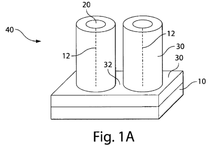
FIG. 1 A includes a schematic illustration of two-phase article 40. A
plurality of
nanostructures 20 is provided such that the long axes of the nanostructures,
indicated by
dashed lines 12, are substantially aligned relative to each other. Each
nanostructure is
positioned relative to an adjacent nanostructure at a distance so as to
together define an
average distance between adjacent nanostructures. Conformal coating 30 may be
formed
on the nanostructures 20 as well as on portions of substrate 10. As noted
above, an
advantage of some embodiments described herein is the ability to form
conformal
coatings on nanostructures having high density and/or aspect ratio. In cases
where the
density of nanostructures on a surface is such that at least some of the
substrate surface is
not covered with nanostructures, the conformal coating may substantially coat
the
exposed portions of the substrate surface as well. As shown in FIG. 1 A,
conformal
coating can be formed along a substantial length (e.g., entire length) of
nanostructures 20
and on portions 32 of the substrate, positioned in areas between closely
packed, high
aspect ratio nanostructures.
In some cases, the substrate may be substantially non-planar, with the
plurality of
nanostructures arranged radially around and/or uniformly over a substantial
majority of
the non-planar surface. FIG. 1 B shows an illustrative embodiment in which
nanostructures 50 are arranged on a cylindrical fiber 60, and conformal
coating 70 has
been formed on the nanostructures as well as exposed portions 72 of substrate
60.
In some embodiments, the two-phase article may include an assembly of carbon
nanotubes arranged on a substrate, and a conformal coating formed on the
carbon
nanotubes, wherein the conformal polymer coating comprises a conducting
polymer such
as PEDOT.
Additional components may also be incorporated into articles of the invention,
as
described more fully below. For example, at least one support material may be
associated with the plurality of nanostructures, i.e., as a conformal or non-
conformal
coating. In some embodiments, a "three-phase article" is demonstrated. The
three-phase
article may include a nanostructure assembly (e.g., "first phase"),
conformally coated by
a second material (e.g., "second phase"), as well as an additional support
material (e.g.,
CA 02747168 2011-06-02
WO 2010/120273 PCT/US2009/006352
11
"third phase"). In some embodiments, the support material may comprise a
polymer,
such as a thermoset polymer or a thermoplastic polymer (e.g., epoxy, PTFE).
FIG. 2 illustrates a three-phase article according to one embodiment of the
invention. The three-phase article can include a plurality of nanostructures
80 grown on
substrate 90 and having a conformal coating 100. A support material 110 may be
applied to the coated nanostructures to form a three-phase article. In some
embodiments,
the support material extends substantially along the entire length of the
nanostructures.
The support material may also fill essentially all of the void space between
the
nanostructures. In some embodiments, the support material may not completely
cover
the nanostructures. For instance, the support material may be applied such
that the
nanostructures extend above the surface of the support material.
In other embodiments, the support material may be formed on portions of the
nanostructures. For example, the support material may be formed along a
substantial
length at least some nanostructures. In some embodiments, the support material
may be
formed partially along the length of the nanostructures, for example, leaving
portions of
the nanostructures closest to the substrate surface substantially free of
support material.
In some cases, the support material may be formed as a conformal coating on
the
nanostructures.
In some embodiments, the three-phase article may include an assembly of carbon
nanotubes arranged on a substrate, a conformal coating comprises a conducting
polymer
such as PEDOT formed on the carbon nanotubes, and a support material
comprising a
thermoset or thermoplastic polymer (e.g., epoxy) formed on the conformal
coating.
In one set of embodiments, three-phase articles described herein may be useful
as
high surface area electrochemical devices (e.g., capacitors). For example, as
shown in
FIG. 2, an assembly of electrically conductive nanostructures 80 (e.g.,
nanotubes) may
be arranged on the surface of substrate 90, which may be optionally
electrically
conductive, to provide an electrically active component. A first coating 100
comprising
a dielectric material (e.g., a insulating polymer) may be conformally
positioned on the
electrically conductive nanostructures 80. A second coating 110 comprising an
electrically conductive material may be arranged, conformally or non-
conformally, in
contact with first coating 100, to form another electrically active component,
such that
nanostructures 80 and second coating 110 may be in electrical communication
with one
another through first coating 100. Such an arrangement may provide
electrochemical
CA 02747168 2011-06-02
WO 2010/120273 PCT/US2009/006352
12
devices with active components having high surface area and enhanced
electrical
properties.
Articles described herein may be readily tailored to suit a particular
application.
For example, the aspect ratio, length, diameter, spacing, and type of
nanostructures may
be varied, as well as the type of conformal coating material(s). Articles
having
additional components or phases may also be produced using methods described
herein.
For example, articles including any number of phases may be fabricated in any
arrangement.
Some embodiments (e.g., arrangements such as those described in association
with FIGS. lA-1B and FIG. 2) may allow for relatively efficient operation in
electrodes.
For example, the use of thin nanostructures (e.g., nanotubes) can result in a
large surface
area to volume ratio. Not wishing to be bound by any theory, the relatively
low amount
of bulk volume can reduce the amount of recombination of electrons and holes
as they
are generated in the electrode, which may lead to a relative increase in the
amount of
electrons that are transported away from the electrode. Such operation can
increase the
amount of work done by the electrode, relative to electrodes with larger
amounts of bulk
material.
Some embodiments may find particular use as part of a capacitor (e.g., an
ultracapacitor). Not wishing to be bound by any particular theory, the
capacitance of a
capacitor can be proportional to the electrode surface area and inversely
proportional to
the distance between the electrodes. In some embodiments, conductive layers
(e.g., a
plurality of nanotubes on a conductive substrate, an electrically conductive
layer over a
pluarlity of nanotubes, and the like) can have relatively high surface area.
In addition, in
some embodiments, the distance between conductive layers can be controlled in
some
cases (e.g., by depositing a relatively thin layer of non-conducting polymer
over a
conductive entity such as a plurality of conductive nanostructures) such that
it is
relatively small (e.g., less than about 80 nm, less than about 60 rim, less
than about
40 rim, less than about 30 rim, less than about 20 rim, less than about 10
rim, less than
about 5 rim, less than about 1 rim, or smaller). Such embodiments can produce
capacitors with relatively high capacitance.
Methods for producing the articles and materials described herein are also
provided. The methods may include providing a plurality of nanostructures, as
described
herein, and forming a conformal coating on the nanostructures. The
nanostructures may
CA 02747168 2011-06-02
WO 2010/120273 PCT/US2009/006352
13
be arranged such that the long axes of the nanostructures are substantially
aligned
relative to each other. In some cases, the nanostructures may be fabricated by
uniformly
growing the nanostructures on the surface of a substrate, such that the long
axes are
aligned and non-parallel to the substrate surface (e.g., substantially
perpendicular to the
substrate surface). In some cases, the long axes of the nanostructures are
oriented in a
substantially perpendicular direction with respect to the surface of a
substrate, forming a
nanostructure "forest." In some embodiments, at least some of the
nanostructures may
have a length (e.g., a dimension along the long axis of the nanostructure) of
at least 10
microns.
The nanostructures may be catalytically formed on the surface of a substrate.
For
example, a nanostructure precursor material (e.g., a hydrocarbon gas such as
C2H4, H2,
hydrogen, argon, nitrogen, combinations thereof, and the like) may be
contacted with a
catalyst material (e.g., nanoparticles of Fe), for example, positioned on the
surface of a
substrate. Examples of suitable nanostructure fabrication techniques are
discussed in
more detail in International Patent Application Serial No. PCT/US2007/0 1 1 9
1 4, filed
May 18, 2007, entitled "Continuous Process for the Production of
Nanostructures
Including Nanotubes," published as WO 2007/136755 on November 29, 2007, and
International Patent Application Serial No. PCT/US2007/011913, filed May 18,
2007,
entitled "Nanostructure-Reinforced Composite Articles," published as
WO/2008/054541,
on May 8, 2008, which are incorporated herein by reference in its entirety.
In some embodiments, the alignment of nanostructures in the nanostructure
"forest" may be substantially maintained, even upon subsequent processing
(e.g.,
application of a force to the forest, conformal coating of the forest,
transfer of the forest
to other surfaces, and/or combining the forests with secondary materials such
as
polymers, metals, ceramics, piezoelectric materials, piezomagnetic materials,
carbon,
and/or fluids, among other materials).
As noted above, conformal coatings may be formed on a plurality of
nanostructures, as well as portions of the substrate on which the
nanostructures are
arranged, i.e., the exposed portions of the substrate. For example, the
conformal coating
may be formed along a substantial length of nanostructures having high aspect
ratio and
on portions of an underlying substrate positioned between adjacent
nanostructures, as
shown in FIGS. 1A and 1B. The conformal coating may be formed using various
methods, including chemical vapor deposition (CVD). That is, the
nanostructures may
CA 02747168 2011-06-02
WO 2010/120273 PCT/US2009/006352
14
be exposed to one or more conformal coating precursors (e.g., monomeric
species) in
vapor phase, such that a conformal coating is formed on the surface of the
nanostructures.
The use of CVD may be advantageous in that substantially uniform coatings may
be formed on a wide range of substrate materials, i.e., formation of conformal
coating
use in CVD may be substrate-independent. Additionally, CVD may be performed at
relatively low temperatures (e.g., less than 500 C, less than 300 C, less
than 100 C,
less than 50 C, less than 30 C). In some embodiments, dry chemical vapor
deposition
methods may be used. Some embodiments involve use of a chemical vapor
deposition
method at room temperature and/or without use of a hot filament to activate
polymerization of monomeric species.
In some embodiments, oxidizing chemical vapor deposition (oCVD) methods
may be used, wherein both an oxidant and a monomeric material are provided in
the
vapor phase for deposition. For example, a solid oxidant may be sublimed in
vapor
phase prior to contacting the nanostructures. In an illustrative embodiment,
an iron
chloride oxidizing agent is heated to 350 C for sublimation process, and the
substrate to
be coated is maintained at 70 C, with a coating duration of about 15 minutes
and a flow
rate of monomer (e.g., EDOT monomer) of 5 sccm.
In some embodiments, initiated chemical vapor deposition (iCVD) methods may
be used, wherein an initiator is included in addition to one or more monomers.
In some
embodiments, relatively low energies can be employed when using an initiator,
which
may be useful when depositing polymer on, for example, relatively delicate
substrates
(e.g., very thin metal foils, tissue paper, etc.). In some such embodiments,
the initiator
can be thermally decomposed. For example, in some cases, an array of
resistively heated
filaments within a vacuum chamber can be heated to drive the pyrolysis of the
initiator
while allowing the substrate to remain cool enough to promote the adsorption
of the
species required for film growth. Examples of suitable initiators can include,
but are not
limited to, perfluorooctane sulfonyl fluoride, triethylamine, tert-butyl
peroxide,
2,2'-azobis (2methylpropane), and benzophenone.
In some embodiments, the formation of a conformal coating does not
substantially change the average distance between adjacent nanostructures or
the
alignment of the nanostructures. For example, prior to the formation of the
conformal
coating, the nanostructures may have a first average distance between adjacent
CA 02747168 2011-06-02
WO 2010/120273 PCT/US2009/006352
nanostructures, and, after formation of the conformal coating, the
nanostructures may
have a second average distance between adjacent nanostructures, wherein the
first and
second average distances are substantially the same. As used herein, average
distances
which are "substantially the same" are differ from one another by less than
10%, less
than 5%, less than 1%, or, in some cases, less than 0.5%. In some cases, the
average
distance may refer to the distance between the centers of adjacent
nanostructures or
coated nanostructures (e.g., distance 82 in FIG. 2). In some cases, the
average distance
may refer to the intertube distance between adjacent coated nanostructures,
i.e., the
distance between outer surfaces or edges of two adjacent coated nanostructures
(e.g.,
distance 84 in FIG. 2).
The formation of a conformal coating may, in some embodiments, change the
average distance between adjacent nanostructures. In some embodiments,
formation of a
conformal coating can reduce the average spacing between nanostructures by at
least
about 10%, at least about 25%, at least about 50%, at least about 75%, at
least about
90%, between about 10% and about 99%, between about 10% and about 90%, between
about 10% and about 75%, between about 10% and about 50%, between about 10%
and
about 25%, between about 25% and about 99%, between about 50% and about 99%,
or
between about 75% and about 99%. The ability to change the average distance
between
adjacent nanostructures can be useful in producing a plurality of
nanostructures with a
relatively close, and in some cases substantially uniform, average distance
between
adjacent nanostructures. For example, in some cases, formation of a conformal
coating
can produce an average spacing between a plurality of nanostructures of less
than about
1 micron, less than about 500 nm, less than about 100 nm, less than about 80
nm, less
than about 60 nm, less than about 40 nm, less than about 30 nm, less than
about 20 nm,
less than about 10 nm, or less than about 5 nm. The ability to produce
uniformly closely
spaced nanostructures can be useful, for example, in embodiments where
consistent and
close spacing of the nanostructures, prior to formation of a coating, is
difficult to
achieve. In some embodiments, the thickness of the conformal coating may be
selected
(e.g., by varying a coating formation parameter such as temperature, pressure,
type of
coating precursor, or concentration of coating precursor) to achieve a
predetermined
average spacing between adjacent coated nanostructures.
The ability to control the average distance between adjacent nanostructures
(e.g.,
via deposition of a conformal polymer coating) can allow one to fabricate, for
example,
CA 02747168 2011-06-02
WO 2010/120273 PCT/US2009/006352
16
filters that are able to separate out a specific range of particle sizes
(e.g., nanoparticle
sizes) upon passing a fluid including a wide range of particle sizes through
the
nanostructures. For example, in some embodiments, a flow of a fluid containing
first
and second populations of particles can be established through the plurality
of
nanostructures (e.g., conformally coated nanostructures). The first population
can
include particles with maximum cross-sectional dimensions greater than the
average
distance between adjacent nanostructures, and the second population can
include
particles with maximum cross-sectional dimensions smaller than the average
distance
between adjacent nanostructures. After establishing a flow of a fluid
containing the first
and second populations toward the nanostructures, the first population may be
at least
partially separated from the second population. In some embodiments, at least
a portion
of the first population can be retained by the nanostructures while at least a
portion of the
second population is passed through the nanostructures. In some embodiments,
the first
and second populations can be substantially completely separated.
The embodiments described herein can be used to at least partially separate a
variety of types of particles. For example, in some cases, the particles can
comprise
quantum dots, biological molecules, and the like. As a specific example, some
embodiments can be useful as relatively inexpensive water filters that can be
used to
separate harmful bacteria such as E. coli.
As used herein, the "maximum cross-sectional dimension" refers to the largest
distance between two opposed boundaries of an individual structure (e.g., a
particle) that
may be measured. The "average maximum cross-sectional dimension" of a
plurality of
structures refers to the number average.
In some embodiments (e.g., where stimulus-responsive polymers are used), the
average distance between adjacent nanostructures may change with a variation
in a
stimulus condition (e.g., electromagnetic radiation, temperature, pH, chemical
species
concentration, etc.). In some cases, the polymer may have a first dimension
(e.g.,
thickness) upon exposure to a first stimulus condition, and the polymer may
have a
second dimension (e.g., thickness) that can be different from the first
dimension upon
exposure to a second stimulus condition that is different from the first
stimulus
condition. The change in the dimension of the polymer may produce a change in
the
average distance between adjacent nanostructures. As a specific example, in
some
embodiments, a plurality of nanostructures may have a first average distance
between
CA 02747168 2011-06-02
WO 2010/120273 PCT/US2009/006352
17
adjacent nanostructures at a first pH and a second average distance between
adjacent
nanostructures (that can be different from the first average distance) at a
second pH that
is different from the first pH. In some instances, a plurality of
nanostructures may have a
first average distance between adjacent nanostructures at a first temperature
and a second
average distance between adjacent nanostructures (that can be different from
the first
average distance) at a second temperature that is different from the first
temperature. As
another example, a plurality of nanostructures may have a first average
distance between
adjacent nanostructures upon exposure to a first wavelength of electromagnetic
radiation
and a second average distance between adjacent nanostructures (that can be
different
from the first average distance) upon exposure to a second wavelength of
electromagnetic radiation that is different from the first wavelength of
electromagnetic
radiation. In some embodiments, variations in moisture level, concentration of
a
chemical species, or any other suitable stimulus can be used to produce a
similar effect.
Controlling the average spacing between adjacent nanostructures using a
stimulus
condition can be useful, for example, in creating a tunable filter. In such
embodiments,
the sizes of the particles that are separated can be dependent upon the
stimulus condition
to which the nanostructures are exposed. For example, in some embodiments, a
flow of
a fluid containing first, second, and third populations of particles can be
established
through the plurality of nanostructures (e.g., conformally coated
nanostructures). The
first population can include particles with relatively large maximum cross-
sectional
dimensions, the second population can include particles with maximum cross-
sectional
dimensions smaller than the particles in the first population, and the third
population can
include particles with maximum cross-sectional dimensions smaller than the
particles in
the first and second populations. Upon exposing the nanostructures to a first
stimulus
condition (e.g., a first temperature, a first pH, a first wavelength of
electromagnetic
radiation, etc.) a first average distance between adjacent nanostructures can
be
established. The first average distance between adjacent nanostructures can be
smaller
than the maximum cross-sectional dimensions of the particles in the first
population, but
larger than the maximum cross-sectional dimensions of the particles in the
second and
third populations. Upon flowing a fluid mixture of the first, second, and
third
populations through the nanostructures, the first population can be at least
partially
separated from the second and third populations. In some cases, the first
population may
CA 02747168 2011-06-02
WO 2010/120273 PCT/US2009/006352
18
be at least partially retained by the nanostructures while the second and
third populations
are at least partially passed through the nanostructures.
Upon exposure to a second stimulus condition (e.g., a second temperature, a
second pH, a second wavelength of electromagnetic radiation, etc.) a second
average
distance between adjacent nanostructures (e.g., different from the first
average distance
between adjacent nanostructures) can be established. The second average
distance
between adjacent nanostructures can be smaller than the maximum cross-
sectional
dimensions of the particles in the second population, and larger than the
maximum cross-
sectional dimensions of the particles in the third population. Upon flowing a
fluid
containing the second and third populations through the nanostructures, the
second
population may be at least partially separated from the third population. In
some cases,
the second population can be at least partially retained by the nanostructures
while the
third population can be at least partially passed through the nanostructures.
In some
embodiments, substantially complete separation of the second and third
populations can
be achieved. Such a process can be repeated for any number of stimulus
conditions and
can be used to separate (partially or substantially completely) any number of
populations
of particles.
Some embodiments of the invention may further comprise treating the
nanostructures, for example, to change the density of the nanostructures. In
some cases,
the densification (e.g., uniaxial or biaxial densification) is performed prior
to forming the
conformal coating on the nanostructures. The nanostructure assembly be treated
via
chemical, mechanical, or other methods, to change (e.g., increase, decrease)
the average
distance between adjacent nanostructures. For example, the nanostructures
treated by
mechanical means to increase the density of nanostructures, and may
subsequently be
conformally coated as described above. Methods for changing the density of
nanostructures are described in U.S. Provisional Patent Application Serial No.
61/114,967, filed November 14, 2008, entitled "Controlled-Orientation Films
and
Nanocomposites Including Nanotubes or Other Nanostructures," which is
incorporated
herein by reference.
In some instances, a force with a component normal to the long axes of the
nanostructures may be applied to the plurality of nanostructures reduce their
spacing, i.e.,
to reduce the average distance between adjacent nanostructures. In some
embodiments, a
second force may be applied to the nanostructures. The second force may
include a
CA 02747168 2011-06-02
WO 2010/120273 PCT/US2009/006352
19
second component that is normal to the long axes of the nanostructures and
orthogonal to
the first component of the first force. The method may also include additional
densification steps, if needed. Application of such force(s) may produce a
material
comprising a high volume fraction or mass density of nanostructures.
The force described herein may be applied using any method known in the art.
In
some embodiments, a mechanical tool is used to apply the force to the
plurality of
nanostructures. For example, an operator may apply a flat surface of a tool
(e.g., a
plastic plunger) against the side of a plurality of nanostructures, and
compress the
nanostructures by hand. In some embodiments, the force may be applied using
compression springs. For example, the plurality of nanostructures may be
situated in an
enclosed or semi-enclosed containment structure with one or more compression
springs
situated between the side of the plurality of nanostructures and an adjacent
wall of the
containment structure. Forces may be applied using other elements including,
but not
limited to, weights, machine screws, and/or pneumatic devices, among others.
For
example, in one set of embodiments, a plurality of nanostructures is arranged
between
two plates. A device (e.g., a machine screw, a spring, etc.) may be used to
apply
pressure against the sides of the nanostructures via the plates. In the case
of a machine
screw, for example, the nanostructures may be compressed between the plates
upon
rotating the screw. In still other embodiments, a liquid may be applied to the
plurality of
nanostructures and dried; upon drying, capillary forces may pull the
nanostructures
together, resulting in a reduction of the average distance between
nanostructures. Other
methods of applying forces to the plurality of nanostructures can be
envisioned by one of
ordinary skill in the art.
The application of a first and/or second force may reduce the average distance
between adjacent nanostructures by varying amounts. In some cases, the average
distance between adjacent nanostructures is reduced by at least about 25%. In
some
instances, the average distance between adjacent nanostructures is reduced by
at least
about 50%, at least about 70%, at least about 80%, at least about 90%, at
least about
95%, at least about 99%, or more.
As noted above, the methods described herein may be used to produce materials
with high volume fractions of nanostructures. As used herein, the volume
fraction of
nanostructures within a material (e.g., a plurality of nanostructures, a
nanocomposite,
etc.) is calculated by dividing the sum of the volumes defined by the
nanostructures by
CA 02747168 2011-06-02
WO 2010/120273 PCT/US2009/006352
the total volume defined by the material. It should be noted that the volume
defined by a
nanostructure may contain some void space. For example, in the case of a
hollow
nanotube, the volume defined by the nanotube would include the interior void
space
within the tube.
Additional components may be incorporated within articles described herein. In
some cases, at least one support material may be applied to the nanostructures
to provide
mechanical, chemical, or an otherwise stabilizing support for the plurality of
nanostructures. In some cases, the support material may be a monomer, a
polymer, a
fiber, a ceramic, or a metal, and may be further processed to support the
nanostructures.
In some embodiments, a support material precursor may be added to the
nanostructures
and may be treated to form a support material associated with the
nanostructures. For
example, a mixture of monomeric species may be added to the nanostructures,
and
subsequent polymerization of the monomeric species may produce a polymer
matrix
comprising the nanostructures disposed therein. In another example, a
polymeric species
may be added to the nanostructures, and subsequent hardening of the polymeric
species
may produce a polymer matrix comprising the nanostructures disposed therein.
Examples of suitable support materials are described more fully below.
The support material precursor may be added to the nanostructures using
various
methods. In some embodiments, the support material precursor may be
transported
between the nanostructures via capillary forces. For example, the
nanostructure
assembly (e.g., nanotube "forest") may contact the surface of a pool or
solution of the
support material precursor, such that the support material precursor infuses
into the
nanostructure assembly, filling in the spaces between individual
nanostructures while
maintaining alignment of and spacing between the nanostructures. In some
cases, the
nanostructure assembly may be submerged within the support material precursor.
Capillary-induced wetting may be performed at various rates, depending on the
characteristics of the nanostructures assembly (e.g., volume fraction, surface
conditions)
and the type of support material (e.g., viscosity). In some embodiments,
articles
comprising nanostructures of lengths exceeding 1 mm and volume fractions
greater than
20% may be wetted with support material, or precursors thereof. In an
illustrative
embodiment, the plurality of nanocomposites is transported by a z-stage and
submerged
in a pool of epoxy precursor. The epoxy precursor is transported between
nanostructures
via capillary action, and the nanostructures are removed from the epoxy pool.
In other
CA 02747168 2011-06-02
WO 2010/120273 PCT/US2009/006352
21
embodiments, the support material precursor may be transported between the
nanostructures by pressure driven flow, molding, or any other known technique.
In other embodiments, the support material precursor may be solidified or
hardened using any suitable method. The epoxy may be cured, for example, by
allowing
the precursor material to set, or optionally by applying heat. In some
embodiments,
hardening may comprise the polymerization of the support material precursor.
In some cases, the support material precursor may be applied to a plurality of
nanostructures that form a self-supporting structure, or the support material
precursor
may be applied to a plurality of nanostructures that are attached to a
substrate. In
addition, nanostructures may be solidified while attached to or apart from a
substrate
and/or any other support material.
In some cases, the nanostructures are dispersed substantially uniformly within
the
hardened support material. For example, the nanostructures may be dispersed
substantially uniformly within at least 10% of the hardened support material,
or, in some
cases, at least 20%, 30%, 40%, 50%, 60%, 70%, 80%, 90%, 95%, or. 100% of the
hardened support material. As used herein, "dispersed uniformly within at
least X% of
the hardened support material" refers to the substantially uniform arrangement
of
nanostructures within at least X% of the volume of the hardened support
material. The
ability to arrange nanostructures essentially uniformly throughout structures
comprising
plurality of fibers allows for the enhanced mechanical strength of the overall
structure.
The nanostructures may be further treated to improve the properties of the
nanostructure material at any step of the fabrication process. In some cases,
the
nanostructures may be annealed.
In some cases, the method may comprise the act of removing the nanostructures
from a substrate. In some cases, the nanostructures may be covalently bonded
to the
substrate, and the removal step comprises breaking at least some of the
covalent bonds.
The act of removing may comprise transferring the nanostructures directly from
the
surface of a first substrate (e.g., a growth substrate) to a surface of a
second substrate
(e.g., a receiving substrate). Removal of the nanostructures may comprise
application of
a mechanical tool, mechanical or ultrasonic vibration, a chemical reagent,
heat, or other
sources of external energy, to the nanostructures and/or the surface of the
substrate. For
example, a scraping ("doctor") or peeling blade, and/or other means such as an
electric
field may be used to initiate and continue delamination of the nanostructures
from the
CA 02747168 2011-06-02
WO 2010/120273 PCT/US2009/006352
22
substrate. In some cases, the nanostructures may be removed by application of
compressed gas, for example. In some cases, the nanostructures may be removed
(e.g.,
detached) and collected in bulk, without attaching the nanostructures to a
receiving
substrate, and the nanostructures may remain in their original or "as-grown"
orientation
and conformation (e.g., in an aligned "forest") following removal from the
substrate.
In one set of embodiments, the attachment between the nanostructures and a
substrate may be altered by exposing the nanostructures and/or substrate to a
chemical
(e.g., a gas). Exposing the nanostructures and/or substrate to the chemical
may, in some
cases, substantially reduce the level of attachment or adhesion between the
nanostructures and the substrate. Examples of chemicals that are useful in
reducing the
level of attachment between the nanostructures and the substrate include, but
are not
limited to, hydrogen, oxygen, and air, among others. In some cases, elevated
temperatures (e.g., temperatures greater than about 100 C) may be used to
expedite the
detachment of nanostructures from the substrate. For example, nanostructures
(e.g.,
carbon nanotubes) may be grown on a substrate and subsequently exposed to
hydrogen
gas while they remain in the processing chamber. Exposing the nanostructures
to
hydrogen may, in some cases, result in the delamination of the nanostructures
from the
substrate. In some embodiments, exposing the nanostructures to hydrogen may
not
result in the complete delamination of the plurality of nanostructures, but
may, for
example, result in the breaking of a large enough fraction of the bonds such
that the force
required to remove the plurality of nanostructures is reduced by at least
about 50%, at
least about 70%, at least about 90%, at least about 95%, at least about 99%,
or more.
Removal of the nanostructures may also comprise application of a mechanical
tool, mechanical or ultrasonic vibration, a chemical reagent, heat, or other
sources of
external energy, to the nanostructures and/or the surface of the substrate. In
some cases,
the nanostructures may be removed by application of compressed gas, for
example. In
some cases, the nanostructures may be removed (e.g,. detached) and collected
in bulk,
without attaching the nanostructures to a receiving substrate, and the
nanostructures may
remain in their original or "as-grown" orientation and conformation (e.g., in
an aligned
"forest") following removal from the substrate.
An external force may be used to initiate and continue delamination of the
layer
from the first substrate, and to direct the layer toward the second substrate.
For example
a scraping ("doctor") or peeling blade, and/or other means such as an electric
field may
CA 02747168 2011-06-02
WO 2010/120273 PCT/US2009/006352
23
be used to initiate and continue delamination. In some cases, the layer may be
delaminated and/or handled as a film, tape, or web. Alternatively, the film
may be
suspended, handled, and optionally mechanically (e.g., rolled, compacted,
densified),
thermally or chemically (e.g., purified, annealed) treated in a continuous
fashion prior to
being transferred to the second substrate.
Methods described herein may be used to control the dimensions and other
properties of a plurality of nanostructures. As described herein, the
nanostructures may
be coated conformally with a material that imparts a particular property
(e.g., electrical
property) onto the nanostructures. In some embodiments, a plurality of
nanostructures
may be provided such that the long axes of the nanostructures are
substantially aligned,
and the plurality has a thickness defined by the long axes of the
nanostructures (e.g., by
the average length of the long axes of the nanostructures). The average length
of the
long axes of the plurality of nanostructures may be controlled, for example,
by adjusting
parameters (e.g., type of reactant used, time over which the nanostructures
are grown,
etc.) of the growth process. In some cases, the average length of the long
axes of the
plurality of nanostructures may be controlled by a post processing step such
as polishing
(e.g., chemical-mechanical polishing), chemical treatment, or some other step.
In some
embodiments, the average spacing between adjacent nanostructures may be
controlled by
the application of a force with a component normal to the long axes of the
nanostructures.
In some embodiments, the conformal coating, as well as the length, thickness,
and density of the nanostructures are together selected to form an article
having a desired
level of absorption of electromagnetic radiation, conductivity, resistance,
modulus, or
some other property. Articles described herein may also comprise tunable multi-
functional properties. For example,
As noted above, the presence of nanostructures within articles described
herein
may impart desirable properties such as improved mechanical strength and/or
toughness,
thermal and/or electrical conductivity, heat transfer, and surface
characteristics (e.g.,
hydrophobicity, hydrophilicity). For example, in some cases a composite
material may
exhibit a higher mechanical strength and/or toughness when compared to an
essentially
identical material lacking the set of substantially-aligned nanostructures,
under
essentially identical conditions, while the alignment or morphology of
nanostructures
remain essentially unaffected. In some embodiments, the nanostructures may be
CA 02747168 2011-06-02
WO 2010/120273 PCT/US2009/006352
24
arranged to enhance the intralaminar interactions of components within a
material or
substrate, to enhance the interlaminar interactions of two substrates or plies
within a
composite structure, or to mechanically strengthen or otherwise enhance the
binding
between the two substrates, among other functions. In some cases, the thermal,
electrical
conductivity, and/or other properties (e.g., electromagnetic properties,
specific heat, etc.)
of articles described herein may be selected to be directionally dependent
(e.g.,
anisotropic).
As used herein, the term "nanostructure" refers to elongated chemical
structures
having a diameter on the order of nanometers and a length on the order of
microns to
millimeters or more, resulting in an aspect ratio greater than 10, 100, 1000,
10,000, or
greater. The term "long axis" is used to refer to the imaginary line drawn
parallel to the
longest length of the nanostructure and intersecting the geometric center of
the
nanostructure. In some cases, the nanostructures may have an average diameter
of less
than about 1 m, less than about 500 nm, less than about 250 nm, less than
about
100 nm, less than about 75 nm, less than about 50 nm, less than about 25 nm,
less than
about 10 nm, or, in some cases, less than about 1 nm. In some instances, the
nanostructure has a cylindrical or pseudo-cylindrical shape. The nanostructure
may be,
for example, a nanotube (e.g., a carbon nanotube), a nanowire, or a nanofiber,
among
others. In some embodiments, the nanostructures used in the systems and
methods
described herein may be grown on a substrate. In other embodiments, the
nanostructures
may be provided separately from the substrate, either attached to another
substrate, or as
a self-supporting structure detached from any substrate.
In some embodiments, the articles and methods described herein comprise
carbon-based nanostructures. Examples of carbon-based nanostructures include
carbon
nanotubes, carbon nanowires, carbon nanofibers, and the like. It should be
understood
that the nanostructures described herein may include atoms other than carbon.
Materials described herein may also be formed over a large surface area. In
some
embodiments, the originally provided plurality of nanostructures extends a
distance at
least 10 times greater than the average distance between adjacent
nanostructures in each
of two orthogonal directions, each direction perpendicular to the long axes.
In some
cases, the plurality of nanostructures extends, in two orthogonal directions
each
perpendicular to the long axes, a distance at least 100 times greater, at
least 1000 times
CA 02747168 2011-06-02
WO 2010/120273 PCT/US2009/006352
greater, at least 10,000 times greater, at least 100,000 times greater, at
least 1,000,000
times greater, or longer than the average distance between adjacent
nanostructures.
In some embodiments, the plurality of nanostructures may be provided as a self-
supporting material. In other cases, the nanostructures may be attached to a
substrate
(e.g., a growth substrate). In some embodiments, the long axes of the
nanostructures are
substantially aligned and non-parallel to the substrate surface, having a
thickness defined
by the long axes of the nanostructures.
The nanostructures may comprise any desirable aspect ratio. In some cases, a
plurality of nanostructures may be provided such that the plurality extends,
in at least one
dimension (e.g., in one dimension, in two orthogonal dimensions, etc.)
substantially
perpendicular to the long axes, a distance at least about 1.5 times greater,
at least about 2
times greater, at least about 5 times greater, at least about 10 times
greater, at least about
25 times greater, at least about 100 times greater, or more than a dimension
substantially
parallel to the long axes of the nanostructures. As a specific example, the
plurality of
nanostructures may constitute a thin-film such that the long axes of the
nanostructures
are substantially perpendicular to the largest surface of the film. A
plurality of
nanostructures may be provided, in some instances, such that the plurality
extends, in at
least one dimension substantially parallel to the long axes, a distance at
least about 1.5
times greater, at least about 2 times greater, at least about 5 times greater,
at least about
10 times greater, at least about 25 times greater, at least about 100 times
greater, or more
than a dimension substantially perpendicular to the long axes of the
nanostructures.
In some cases, at least 10%, at least about 20%, at least about 30%, at least
about
40%, at least about 50%, at least about 60%, at least about 70%, or more of
the
nanostructures extend substantially through thickness of the plurality of
nanostructures.
As used herein, the term "nanotube" is given its ordinary meaning in the art
and
refers to a substantially cylindrical molecule or nanostructure comprising a
fused
network of primarily six-membered aromatic rings. In some cases, nanotubes may
resemble a sheet of graphite formed into a seamless cylindrical structure. It
should be
understood that the nanotube may also comprise rings or lattice structures
other than six-
membered rings. Typically, at least one end of the nanotube may be capped,
i.e., with a
curved or nonplanar aromatic group. Nanotubes may have a diameter of the order
of
nanometers and a length on the order of millimeters, or, on the order of
tenths of
microns, resulting in an aspect ratio greater than 100, 1000, 10,000, or
greater. In some
CA 02747168 2011-06-02
WO 2010/120273 PCT/US2009/006352
26
cases, the nanotube is a carbon nanotube. The term "carbon nanotube" refers to
nanotubes comprising primarily carbon atoms and includes single-walled
nanotubes
(SWNTs), double-walled CNTs (DWNTs), multi-walled nanotubes (MWNTs) (e.g.,
concentric carbon nanotubes), inorganic derivatives thereof, and the like. In
some
embodiments, the carbon nanotube is a single-walled carbon nanotube. In some
cases,
the carbon nanotube is a multi-walled carbon nanotube (e.g., a double-walled
carbon
nanotube). In some cases, the nanotube may have a diameter less than I m,
less than
100 nm, 50 nm, less than 25 nm, less than 10 nm, or, in some cases, less than
1 nm. In
one set of embodiments the nanotubes have an average diameter of 50 nm or
less, and
are arranged in composite articles as described herein. The inorganic
materials include
semiconductor nanowires such as silicon (Si) nanowires, indium-gallium-
arsenide
(InGaAs) nanowires, and nanotubes comprising boron nitride (BN), silicon
nitride
(Si3N4), silicon carbide (SiC), dichalcogenides such as (WS2), oxides such as
titanium
dioxide (Ti02) and molybdenum trioxide (MoO3), and boron-carbon-nitrogen
compositions such as BC2N2 and BC4N.
Substrates suitable for use in the invention include prepregs, polymer resins,
dry
weaves and tows, inorganic materials such as carbon (e.g., graphite), metals,
alloys,
intermetallics, metal oxides, metal nitrides, ceramics, and the like. In some
cases, the
substrate may be a fiber, tow of fibers, a weave, and the like. The substrate
may further
comprise a conducting material, such as conductive fibers, weaves, or
nanostructures. In
some embodiments, the substrates used herein are substantially transparent to
electromagnetic radiation. For example, in some cases, the substrate may be
substantially transparent to visible light, ultraviolet radiation, or infrared
radiation. In
other cases, the nanostructures may be provided as a self-supporting structure
free of a
substrate and/or any other material. In some embodiments, the substrate may
comprise
alumina, silicon, carbon, a ceramic, or a metal.
In some cases, the substrate may be hollow and/or porous. In some
embodiments, the substrate is porous, such as a porous A1203. As used herein,
a
"porous" material is defined as a material having a sufficient number of pores
or
interstices such that the material is easily crossed or permeated by, for
example, a fluid
or mixture of fluids (e.g., liquids, gases). In some embodiments, the
substrate is a fiber
comprising A1203, Si02, or carbon. In some embodiments, the substrate may
comprise a
CA 02747168 2011-06-02
WO 2010/120273 PCT/US2009/006352
27
layer, such as a transition metal oxide (A1203) layer, formed on surface of an
underlying
material, such as a metal or ceramic.
In some cases, the substrates as described herein may be prepregs, that is, a
polymer material (e.g., thermoset or thermoplastic polymer) containing
embedded,
aligned, and/or interlaced (e.g., woven or braided) fibers such as carbon
fibers. As used
herein, the term "prepreg" refers to one or more layers of thermoset or
thermoplastic
resin containing embedded fibers, for example fibers of carbon, glass, silicon
carbide,
and the like. In some embodiments, thermoset materials include epoxy, rubber
strengthened epoxy, BMI, PMK-15, polyesters, vinylesters, and the like, and
preferred
thermoplastic materials include polyamides, polyimides, polyarylene sulfide,
polyetherimide, polyesterimides, polyarylenes, polysulfones,
polyethersulfones,
polyphenylene sulfide, polyetherimide, polypropylene, polyolefins,
polyketones,
polyetherketones, polyetherketoneketone, polyetheretherketones, polyester, and
analogs
and mixtures thereof. Typically, the prepreg includes fibers that are aligned
and/or
interlaced (woven or braided) and the prepregs are arranged such the fibers of
many
layers are not aligned with fibers of other layers, the arrangement being
dictated by
directional stiffness requirements of the article to be formed by the method.
The fibers
generally can not be stretched appreciably longitudinally, thus each layer can
not be
stretched appreciably in the direction along which its fibers are arranged.
Exemplary
prepregs include TORLON thermoplastic laminate, PEEK (polyether etherketone,
Imperial Chemical Industries, PLC, England), PEKK (polyetherketone ketone,
DuPont)
thermoplastic, T800H/3900-2 thermoset from Toray (Japan), and AS4/3501-6
thermoset
from Hercules (Magna, Utah).
Substrates described herein may be any material capable of supporting catalyst
materials and/or nanostructures as described herein. The substrate may be
selected to be
inert to and/or stable under sets of conditions used in a particular process,
such as
nanostructure growth conditions, nanostructure removal conditions, and the
like. In
some embodiments, the substrate may be selected to be conductive. In some
cases, the
substrate comprises a substantially flat surface. In some cases, the substrate
comprises a
substantially nonplanar surface. For example, the substrate may comprise a
cylindrical
surface (e.g., fiber).
As described herein, the invention may comprise use or addition of one or more
binding materials or support materials. The binding or support materials may
be
CA 02747168 2011-06-02
WO 2010/120273 PCT/US2009/006352
28
polymer materials, fibers, metals, or other materials described herein.
Polymer materials
for use as binding materials and/or support materials, as described herein,
may be any
material compatible with nanostructures. For example, the polymer material may
be
selected to uniformly "wet" the nanostructures and/or to bind one or more
substrates. In
some cases, the polymer material may be selected to have a particular
viscosity, such as
50,000 cPs or lower, 10,000 cPs or lower, 5,000 cPs or lower, 1,000 cPs or
lower, 500
cPs or lower, 250 cPs or lower, or 100 cPs or lower. In some embodiments, the
polymer
material may be selected to have a viscosity between 150-250 cPs. In some
cases, the
polymer material may be a thermoset or thermoplastic. In some cases, the
polymer
material may optionally comprise a conducting material, including conductive
fibers,
weaves, or nanostructures.
Examples of thermosets include Microchem SU-8 (UV curing epoxy, grades
from 2000.1 to 2100, and viscosities ranging from 3 cPs to 10,000 cPs),
Buehler Epothin
(low viscosity, -150 cPs, room temperature curing epoxy), West Systems 206 +
109
Hardener (low viscosity, -200 cPs, room temperature curing epoxy), Loctite
Hysol 1 C
(20-min curing conductive epoxy, viscosity 200,000 - 500,000cPs), Hexcel RTM6
(resin
transfer molding epoxy, viscosity during process -10 cPs), Hexcel HexFlow VRM
34
(structural VARTM or vacuum assisted resin transfer molding epoxy, viscosity
during
process -500 cPs). Examples of thermoplastic include polystyrene, or Microchem
PMMA (UV curing thermoplastic, grades ranging from 10 cPs to 1,000 cPs).In one
embodiment, the polymer material may be PMMA, EpoThin, WestSystems EPON,
RTM6, VRM34, 977-3, SU8, or Hysol I C.
In some cases, the support material may be a monomeric species and/or a
polymer comprising cross-linking groups, such that polymerization and/or cross-
linking
of the polymers may form a hardened structure comprising the aligned
nanostructures.
In other embodiments, the support material may be a metal or a metal powder
such as a
metal nanoparticles having diameter on the order of the diameter of the
nanostructures or
the spacing between the nanostructures on the substrate. The metal may be
softened,
sintered, or melted when added to the aligned nanostructures, such that
cooling of the
metal may form a metal structure comprising the aligned nanostructures. As
used herein,
an "integrally self-supporting structure" is defined as a non-solid structure
having
sufficient stability or rigidity to maintain its structural integrity (e.g.,
shape) without
external support along surfaces of the structure. Solid and/or self-supporting
structures
CA 02747168 2011-06-02
WO 2010/120273 PCT/US2009/006352
29
comprising aligned nanostructures may be useful as substrate or other
components for
composite materials, as described herein.
Polymers or polymer materials, as used herein, refer to extended molecular
structures comprising a backbone (e.g., non-conjugated backbone, conjugated
backbone)
which optionally contain pendant side groups, where "backbone" refers to the
longest
continuous bond pathway of the polymer. In one embodiment, at least a portion
of the
polymer is conjugated or pi-conjugated, i.e. the polymer has at least one
portion along
which electron density or electronic charge can be conducted, where the
electronic
charge is referred to as being "delocalized." Each p-orbital participating in
conjugation
can have sufficient overlap with adjacent conjugated p-orbitals. In one
embodiment, at
least a portion of the backbone is conjugated. In one embodiment, a
substantial majority
of the backbone is conjugated and the polymer is referred to as a "pi-
conjugated
polymer" or "conjugated polymer." Polymers having a conjugated pi-backbone
capable
of conducting electronic charge may be referred to as "conducting polymers."
In some
cases, the conjugated pi-backbone may be defined by a plane of atoms directly
participating in the conjugation, wherein the plane arises from a preferred
arrangement of
the p-orbitals to maximize p-orbital overlap, thus maximizing conjugation and
electronic
conduction. In some cases, the pi-backbone may preferably have a non-planar or
twisted
ground state conformation, leading to decreased conjugation and a higher
energy
conduction band.
The polymer can be a homo-polymer or a co-polymer such as a random co-
polymer or a block co-polymer. In one embodiment, the polymer is a block co-
polymer.
An advantageous feature of block co-polymers is that they may mimic a multi-
layer
structure, wherein each block may be designed to have different band gap
components
and, by nature of the chemical structure of a block co-polymer, each band gap
component is segregated. As described herein, the band gap and/or selectivity
for
particular analytes can be achieved by modification or incorporation of
different polymer
types. The polymer compositions can vary continuously to give a tapered block
structure
and the polymers can be synthesized by either step growth or chain growth
methods.
The following applications and patents are incorporated herein by reference in
their entirety for all purposes: International Patent Application Serial No.
PCT/US2007/011914, filed May 18, 2007, entitled "Continuous Process for the
Production of Nanostructures Including Nanotubes," published as WO 2007/136755
on
CA 02747168 2011-06-02
WO 2010/120273 PCT/US2009/006352
November 29, 2007; International Patent Application Serial No. PCT/US07/11913,
filed
May 18, 2007, entitled "Nanostructure-reinforced Composite Articles and
Methods,"
published as WO 2008/054541 on May 8, 2008; U.S. Patent Application Serial No.
11/386,378, filed March 22, 2006, entitled "Nano-Engineered Material
Architectures:
Ultra-Tough Hybrid Nanocomposite System"; U.S. Patent Application Serial No.
11/895,621, filed August 24, 2007, entitled "Nanostructure-Reinforced
Composite
Articles," published as U.S. Patent Application Publication No. 2008/0075954
on March
27, 2008; International Patent Application Serial No. PCT/US2008/009996, filed
August
22, 2008, entitled "Nano structure-reinforced Composite Articles and Methods,"
published as WO 2009/029218 on March 5, 2009; U.S. Patent No. 7,537,825,
issued on
May 26, 2009, entitled "Nano-Engineered Material Architectures: Ultra-Tough
Hybrid
Nanocomposite System;" U.S. Provisional Patent Application Serial No.
61/114,967,
filed November 14, 2008, entitled "Controlled-Orientation Films and
Nanocomposites
Including Nanotubes or Other Nanostructures;" U.S. Patent Application Serial
No.
12/618,203, filed November 13, 2009, entitled "Controlled-Orientation Films
and
Nanocomposites Including Nanotubes or Other Nanostructures;" U.S. Provisional
Patent
Application Serial No. 61/119,673, filed on December 3, 2008, entitled
"Multifunctional
Composites Based on Coated Nanostructures;" U.S. Provisional Patent
Application
61/230,267, filed July 31, 2009, entitled "Systems and Methods Related to the
Formation
of Carbon-Based Nanostructures;" and U.S. Provisional Patent Application
61/264,506,
filed November 25, 2009, entitled "Systems and Methods for Enhancing Growth of
Carbon-Based Nanostructures;" each of which is incorporated herein in its
entirety.
The following examples are intended to illustrate certain embodiments of the
present invention, but do not exemplify the full scope of the invention.
EXAMPLES
Example 1
This example demonstrates the fabrication of a two-phase composite of CNTs
and conducting polymers. The fabrication process is shown schematically in
FIG. 19,
wherein (1) carbon nanotubes are grown on a silicon substrate, (2) a conformal
polymer
coating is formed on the carbon nanotubes and silicon substrate, (3) the
coated carbon
nanotubes are removed from the substrate, and (3) characterization using SEM,
TEM,
FTIR, and other methods, is performed.
CA 02747168 2011-06-02
WO 2010/120273 PCT/US2009/006352
31
Multi-walled carbon nanotubes (MWNTs) were grown by thermal chemical
vapor deposition (CVD) method on silicon wafers using a thin catalyst layer of
Fe/A1203
(1/10 nm) deposited by electron beam evaporation. CNT growth was performed in
a
quartz tube furnace (22 mm ID) at atmospheric pressure. Ethylene was employed
as the
source of carbon for obtaining the CNTs. The typical growth temperature was
750 C,
and the growth rate was 2 microns/second. Typically, CNT forests were grown on
1 cm2
silicon wafers, which resulted in well aligned CNTs having densities of about
109-1010
CNTs/cm2. Following the growth of CNTs, a H2/He gas mixture was flushed at 750
C
for 5 min to achieve easier delamination of CNTs arrays from Si substrate.
Deposition of PEDOT on CNT arrays was accomplished using the oxidative
chemical vapor deposition process (oCVD). Briefly, the CNT arrays were held
face
down in a vacuum chamber, facing the oxidizing agent. Mere heating of the
oxidizing
agent allowed for its sublimation onto the substrate. Further reaction of this
incoming
oxidizing agent with the EDOT monomer (supplied through the vapor phase)
resulted in
the formation of PEDOT film on the CNT array substrate. All PEDOT deposition
experiments were performed at a substrate temperature of 70 T. The samples
were
gently rinsed in isopropanol following PEDOT deposition to remove any excess
oxidizing agent present on the samples.
A scanning electron cross-sectional micrograph of PEDOT coated CNT arrays is
presented in FIG. 3. As observed in FIG. 3, the orientation and the shape of
the CNT
array was not disturbed by the oCVD PEDOT coating process. In order to confirm
that
each individual CNT was coated with PEDOT, these CNTs were removed from the
substrate, dispersed in isopropanol, and high resolution microscopy was
performed. A
high magnification image of the dispersed CNTs showed that the diameter of
individual
CNTs was 30 nm after PEDOT deposition (FIG. 4) indicating that there was a 10
nm
PEDOT coating around each nanotube.
To confirm further the presence of PEDOT around the CNTs, energy dispersive
analysis (EDS) was performed along the length of the PEDOT coated CNT array.
Micrographs of PEDOT coated CNT arrays along with a line profile of sulfur are
presented in FIGS. 5 and 6, respectively. The analysis showed the presence of
sulfur
along the length of the array. Further, the concentration of sulfur was found
to be
uniform along the length of the array (FIG. 6). It is worthwhile to note here
that sulfur
comes only from the PEDOT component of the composite.
CA 02747168 2011-06-02
WO 2010/120273 PCT/US2009/006352
32
Transmission electron microscopy before deposition (FIG. 7) and after
deposition
(FIG. 8) also showed that the CNTs are coated with PEDOT. The thick coating at
the
edge of each tube is indicative of the presence of PEDOT around CNTs (FIG. 8).
A high
magnification TEM image shown in the inset to FIG. 8 shows the thickness
contrast
between the edge and the center of a CNT.
Additional evidence that PEDOT conformally coated the CNTs came from the
observed presence of PEDOT on the silicon substrate supporting the CNT arrays,
which
was observed only on the regions of the substrate devoid of any carbon
nanotubes (In
this example, 1% volume fraction CNTs had an inter-tube distance of 80 nm). A
micrograph showing the presence of PEDOT on the silicon substrate after
removal of
CNTs is shown in FIG. 9. The dot pattern observed is indicative of the
presence of
PEDOT on the substrate. FT-IR analysis of the silicon substrate confirmed the
presence
of PEDOT on the substrate. A comparison of an FTIR spectrum of a PEDOT coating
on
top of the silicon substrate (supporting the carbon nanotubes) with an FTIR
spectrum of
a standard PEDOT film deposited on pristine silicon wafers is presented in
FIG. 10. As
observed in FIG. 10, the spectrum of PEDOT present on the silicon substrate
supporting
the carbon nanotubes displayed the modes typically observed in PEDOT films.
The
vibration modes of the C-S bond at 689 cm-1, 842 cm-1 and 979 cm-1 and the
ethylenedioxy ring deformation mode at 922 cm -1 are observed in the spectrum
shown in
FIG. 10. The absence of a C-H mode at 890 cm"1 indicated that the
polymerization
occurred at the 2 and 5 positions.
FIG. 17 shows images of contact angle measurements of water droplets on
various surfaces including (i) un-coated carbon nanotubes, (ii) PEDOT-coated
carbon
nanotubes, and (iii) PEDOT. The resulting contact angle measurements
demonstrated
that the hydrophobicity of PEDOT-coated 1% volume fraction CNTs was
intermediate
(93 ) in comparison to 1% volume fraction CNTs (125 ) and PEDOT coated silicon
(65 )
(FIG. 17). The wetting behavior of the coated carbon nanotubes is also
expected to be
directional dependant.
Example 2
This example demonstrates the fabrication of three-phase composites.
Following the deposition of PEDOT on the CNT arrays, the two-phase
composites were lowered into a pool of epoxy and cured to obtain three-phase
CA 02747168 2011-06-02
WO 2010/120273 PCT/US2009/006352
33
composites (comprising CNTS, PEDOT, and epoxy). CNT forests were biaxially
compressed and then coated with PEDOT. The PEDOT coated forests were then
lowered into a pool of uncured epoxy. An aero grade epoxy, RTM 6 (epoxy has a
viscosity of 33 cP at 90 C), was employed for this purpose. The epoxy infused
into the
CNT arrays through capillary driven wetting. Following the infusion of the
epoxy, the
entire composites were cured at 200 C in air. As-obtained CNT arrays are
referred to as
I% volume fraction, the densified CNT arrays are referred to as 5%, 8%, and
20%
volume fraction. The intertube distance between conformally coated
nanostructures
corresponding to the volume fractions is presented in FIG. 13. As used in this
Example,
the "intertube distance" refers to the distance between the outer surfaces
(e.g., outer
surface of the conformal coating) of two, adjacent conformally coated
nanostructures.
FIG. 16 shows scanning-electron micrograph cross-sectional images of three-
phase composites comprising carbon nanotubes conformally coated with PEDOT,
with
an additional epoxy layer formed on and between the coated carbon nanotubes.
The
three-phase composite was cut and the cross-section was observed under SEM. As
shown in FIG. 16, individual nanostructures can be observed after fabrication
of the
three-phase composite. The diameter of the individual conformally coated
nanotubes
was measured to be about 50 nm, indicating that the carbon nanotubes did not
agglomerate, i.e., were not "bundled up," during the composite fabrication
process.
Rather, the observed diameter of an individual nanostructure indicated the
presence of an
individual carbon nanotube having a diameter of about 10 nm, a PEDOT coating
formed
on the individual carbon nanotube with a thickness of about 10 nm, giving an
overall
outer diameter of the coated nanotube of about 30 nm, and an epoxy component.
Example 3
This example demonstrates the electrical characterization of PEDOT coated CNT
three-phase composites using two-point probe electrical measurements.
In order to understand the electrical behavior of the composites, the change
in the
resistance of the composites with temperature was studied. The resistance
measurements
were performed using two-point probe measurements without the use of any
additional
metal contact pads. The obtained resistances were then converted into
conductivity.
FIG. 11 shows schematic representations of (a) a two-phase composite and (b) a
three-
phase composite, with the radial direction indicated by arrows. FIG. 14 shows
schematic
CA 02747168 2011-06-02
WO 2010/120273 PCT/US2009/006352
34
representations of (a) a two-phase composite and (b) a three-phase composite,
with the
axial direction indicated by arrows.
For a semi-infinite sample, the resistivity (p) can be obtained from the
resistance
(R) using the relationship p = RAIL. Here, L is the distance between the
probes and A is
the cross-sectional area. The conductivity could then be obtained from
resistivity using
the relationship 6 = 1/p. The data along the radial (transverse to CNT long
axis)
direction (FIG. 11) of the composite samples showed that the variation of
resistivity with
temperature followed the VRH model and that the resistivity was proportional
to T-li3
According to the VRH variable range hopping model, conductivity occurs by
hopping of
charge carriers and the resistivity (p) follows the following relationship
with
temperature: p = poe{(To/T)^[1/(n+1)]}. Here, To is the characteristic
temperature and n
is the dimensionality of the conduction. The variation of resistivity with
temperature is
observed to be fit best when n = 3. This result indicated that the
conductivity along the
radial direction in the composites was two-dimensional.
An Arrhenius plot of the variation of conductivity with inverse of temperature
in
the radial direction (FIG. 12A) showed that the activation energy required for
the
creation of mobile charge carriers was inversely proportional to the volume
fraction (i.e.,
proportional to the intertube distance). This activation energy (FIG. 12B) was
also lower
in three-phase composites as compared to two-phase composites. Further, the
decrease
in activation energy between the two-phase and three-phase composites was
higher in
lower volume fraction composites as compared to higher volume fraction
composites.
As the volume fraction of the composites increased (i.e., the intertube
distance
decreased), the effect of the introduction of the conducting polymers on the
activation
energy was expected to be lower than that observed due to the reduction in
intertube
distance. The variation of resistivity with temperature (FIG. 12C) in the
radial direction
indicates that the conductivity is three-dimensional in these composites.
In contrast, in the axial direction, the conduction was primarily along the
length
of the CNTs. (FIG. 15A) Hence, the activation energy was not expected to vary
considerably with variation in intertube distance. As shown in FIG. 15B, the
activation
energy was lower in two-phase composites as compared to three-phase
composites. The
introduction of conducting polymer was also not expected to vary the
activation energy
as the contribution to conductivity was dominated by the CNTs themselves. FIG.
15C
shows a plot of resistivity of various composites as a function of temperature
in the axial
CA 02747168 2011-06-02
WO 2010/120273 PCT/US2009/006352
direction. The activation energies in the axial direction were found to
considerably lower
than those observed in the radial direction (FIG. 12C). The activation
energies were
found to be very low for all samples (0.009 to 0.098 eV) (FIG. 13).
This analysis indicated that the composites exhibited directional dependant
behavior and that the alignment of the CNT forests was not disturbed by the
conducting
polymer deposition process. The wetting behavior of the CNT forests was also
found to
be directional dependant.
Example 4
This example describes the fabrication of three-phase composite including an
Al
cloth (e.g., fibers), carbon nanotubes, and a PEDOT conformal coating. Using
the
methods described herein, a three-phase composite was fabricated by growing
carbon
nanotubes on an Al cloth and then conformally coating the carbon nanotubes and
Al
cloth with PEDOT. FIG. 18A shows an SEM image of an Al cloth with carbon
nanotubes without a conformal polymer coating. FIG. 18B shows SEM images of an
Al
cloth with carbon nanotubes prior to conformally coating with PEDOT (left
images) and
after to conformally coating with PEDOT (right images).
While several embodiments of the present invention have been described and
illustrated herein, those of ordinary skill in the art will readily envision a
variety of other
means and/or structures for performing the functions and/or obtaining the
results and/or
one or more of the advantages described herein, and each of such variations
and/or
modifications is deemed to be within the scope of the present invention. More
generally,
those skilled in the art will readily appreciate that all parameters,
dimensions, materials,
and configurations described herein are meant to be exemplary and that the
actual
parameters, dimensions, materials, and/or configurations will depend upon the
specific
application or applications for which the teachings of the present invention
is/are used.
Those skilled in the art will recognize, or be able to ascertain using no more
than routine
experimentation, many equivalents to the specific embodiments of the invention
described herein. It is, therefore, to be understood that the foregoing
embodiments are
presented by way of example only and that, within the scope of the appended
claims and
equivalents thereto, the invention may be practiced otherwise than as
specifically
described and claimed. The present invention is directed to each individual
feature,
CA 02747168 2011-06-02
WO 2010/120273 PCT/US2009/006352
36
system, article, material, kit, and/or method described herein. In addition,
any
combination of two or more such features, systems, articles, materials, kits,
and/or
methods, if such features, systems, articles, materials, kits, and/or methods
are not
mutually inconsistent, is included within the scope of the present invention.
The indefinite articles "a" and "an," as used herein in the specification and
in the
claims, unless clearly indicated to the contrary, should be understood to mean
"at least
one."
The phrase "and/or," as used herein in the specification and in the claims,
should
be understood to mean "either or both" of the elements so conjoined, i.e.,
elements that
are conjunctively present in some cases and disjunctively present in other
cases. Other
elements may optionally be present other than the elements specifically
identified by the
"and/or" clause, whether related or unrelated to those elements specifically
identified
unless clearly indicated to the contrary. Thus, as a non-limiting example, a
reference to
"A and/or B," when used in conjunction with open-ended language such as
"comprising"
can refer, in one embodiment, to A without B (optionally including elements
other than
B); in another embodiment, to B without A (optionally including elements other
than A);
in yet another embodiment, to both A and B (optionally including other
elements); etc.
As used herein in the specification and in the claims, "or" should be
understood
to have the same meaning as "and/or" as defined above. For example, when
separating
items in a list, "or" or "and/or" shall be interpreted as being inclusive,
i.e., the inclusion
of at least one, but also including more than one, of a number or list of
elements, and,
optionally, additional unlisted items. Only terms clearly indicated to the
contrary, such
as "only one of" or "exactly one of," or, when used in the claims, "consisting
of," will
refer to the inclusion of exactly one element of a number or list of elements.
In general,
the term "or" as used herein shall only be interpreted as indicating exclusive
alternatives
(i.e. "one or the other but not both") when preceded by terms of exclusivity,
such as
"either," "one of," "only one of," or "exactly one of." "Consisting
essentially of," when
used in the claims, shall have its ordinary meaning as used in the field of
patent law.
As used herein in the specification and in the claims, the phrase "at least
one," in
reference to a list of one or more elements, should be understood to mean at
least one
element selected from any one or more of the elements in the list of elements,
but not
necessarily including at least one of each and every element specifically
listed within the
list of elements and not excluding any combinations of elements in the list of
elements.
CA 02747168 2011-06-02
WO 2010/120273 PCT/US2009/006352
37
This definition also allows that elements may optionally be present other than
the
elements specifically identified within the list of elements to which the
phrase "at least
one" refers, whether related or unrelated to those elements specifically
identified. Thus,
as a non-limiting example, "at least one of A and B" (or, equivalently, "at
least one of A
or B," or, equivalently "at least one of A and/or B") can refer, in one
embodiment, to at
least one, optionally including more than one, A, with no B present (and
optionally
including elements other than B); in another embodiment, to at least one,
optionally
including more than one, B, with no A present (and optionally including
elements other
than A); in yet another embodiment, to at least one, optionally including more
than one,
A, and at least one, optionally including more than one, B (and optionally
including other
elements); etc.
In the claims, as well as in the specification above, all transitional phrases
such as
"comprising," "including," "carrying," "having," "containing," "involving,"
"holding,"
and the like are to be understood to be open-ended, i.e., to mean including
but not limited
to. Only the transitional phrases "consisting of' and "consisting essentially
of shall be
closed or semi-closed transitional phrases, respectively, as set forth in the
United States
Patent Office Manual of Patent Examining Procedures, Section 2111.03.
What is claimed is: