Note: Descriptions are shown in the official language in which they were submitted.
CA 02747540 2011-06-17
PCT/JP2008/003870
SPECIFICATION
SOLAR CELL MODULE AND METHOD FOR PRODUCING THE SAME
TECHNICAL FIELD
[0001]
The present invention relates to a solar cell module and its manufacturing
method in which, by adhering a plurality of spherical solar cells to narrow
lead strings of an electrically conductive connecting mechanism and by
adhering a plurality of bypass diodes to wide lead pieces of that electrically
conducting mechanism, these are arranged in the form of a matrix having a
plurality of rows and a plurality of columns, and a transparent panel
member in a pair of panel members is integrally provided at least on an
incident side of sunlight.
BACKGROUND TECHNOLOGY
[0002]
In the prior art, various solar cell modules have already been
implemented in which solar cells are installed in a window material. For the
solar cells installed in these solar cell modules, solar cells made in flat
plate
form from flat silicon crystal plates, or spherical solar cells made from
spherical silicon crystals, or thin layer type solar cells made by forming
layers on a glass substrate or the like have been employed.
[0003]
Now, the inventor of the present application has proposed a spherical
solar cell as disclosed in Patent Document #1. This spherical solar cell
includes a p type or n type spherical silicon single crystal of diameter 1 mm
to 2 mm, a pn junction formed near the outer surface of this spherical silicon
1
CA 02747540 2011-06-17
PCT/JP2008/003870
single crystal and shaped as a partially spherical surface, and positive and
negative electrodes in spot form that respectively make low resistance
contact with center portions of the p type and n type surface regions on
opposite sides of the center of the sphere. Since the positive and negative
electrodes are provided at the two end portions of the solar cell, accordingly
not only is this solar cell capable of receiving light directly incident from
any
direction without any bias, but also the efficiency of utilization of external
light is remarkably enhanced over that of a solar cell which is formed as a
flat plate, since this solar cell can receive light that is reflected or
diffused
from its surroundings.
[0004]
Furthermore, the inventor of the present application has proposed a
solar cell module as disclosed in Patent Document #2. With this solar cell
module, for example, 25 spherical solar cells whose electrically conductive
directions are all aligned are arranged as a matrix form having 5 rows and 5
columns, they are held by an electrically conductive construction made from
six metallic lead frames, and the external periphery thereof is molded with
transparent resin (a covering material). Solar cell modules of similar types
to
the above are also described in Patent Documents #3 and #4.
[0005]
Now, for the spherical solar cells described above, spherical silicon
single crystals of diameter 1 mm to 2 mm are employed in order to enhance
the output per unit weight of the spherical silicon single crystals. Since the
output of each of the spherical solar cells is low (for example approximately
0.5 mW), in order to increase the output of the module, it is necessary to
increase the number of the spherical solar cells that are connected in series
2
CA 02747540 2011-06-17
PCT/JP2008/003870
and the number of the spherical solar cells that are connected in parallel.
However, it is difficult to connect up such a large number of small spherical
solar cells, so that the manufacturing cost is high. For this reason, there is
a
demand for a manufacturing method for connecting up a large number of
spherical solar cells simply and at low cost.
[0006]
Thus, with the method for producing solar cell modules described in
the above Patent Documents #2 to #4, first, five spherical solar cells, with
their electrically conductive directions aligned, are connected at regular
intervals on each of three lead strings that are formed as a flat plate shaped
lead frame. Next, a lead frame of the same shape is mounted over this
structure and is connected to it, and furthermore five spherical solar cells
are
connected to each of the lead strings on this lead frame. Subsequently,
further lead frames and solar cells are successively mounted and connected
in a similar manner to that described above, and thereby three solar cell
groups are manufactured in which the solar cells are arranged in five rows,
and in five columns in the direction orthogonal to the lead frames. And three
solar cell modules are manufactured by resin molding these cell groups.
[0007]
Since, in the solar cell modules described in the above Patent
Documents #2 to #4, the plurality of spherical solar cells are connected in
series and also in parallel by a connection circuit like a mesh, accordingly,
even if the output current of each of the solar cells fluctuates to a certain
extent, it can still be anticipated that the current distribution is equalized
via the parallel connections. And even if a portion of these solar cells are
in
the shade so that their output current decreases, it may be anticipated that
3
CA 02747540 2011-06-17
PCT/JP2008/003870
the current distribution will be equalized in a similar manner.
Patent Document #1: International Publication WO 98/15983;
Patent Document #2: International Publication WO 02/35613;
Patent Document #3: International Publication WO 03/017382;
Patent Document #4: International Publication WO 03/017383.
DISCLOSURE OF THE INVENTION
PROBLEMS TO BE SOLVED BY THE INVENTION
[00081
However while, in the solar cell modules of Patent Documents #2 to
#4 described above, the construction is one in which a plurality of sub
arrays including solar cells are laminated together in several stages, since
the width of the lead strings is made as a fixed width that is narrower than
the radius of the solar cells, accordingly manufacturing by the method of
laminating together the sub arrays in several stages is impossible after the
sub arrays have been assembled. The reason for this is because there are no
portions on the sub arrays by which they can be grasped by the hand of an
automatic assembly device, and also it is not possible to form any
engagement portions that are suitable for setting the positions of the sub
arrays. Due to this, it is necessary to develop a method of some special type
for production, and the manufacturing cost becomes high.
[00091
And since, in the above described manufacturing method for producing
a solar cell module, a plurality of assembled groups each having of a
plurality of rows and a plurality of columns of solar cells are made by
installing a plurality of spherical solar cells between metallic plates that
are
formed with a plurality of lead strings, and thereafter these are held in dies
4
CA 02747540 2011-06-17
PCT/JP2008/003870
and resin molded, accordingly dies of complex structures are required, so
that the manufacturing cost becomes high.
[0010]
Moreover, since it is necessary to insert the dies between the plurality
of assembled groups during the resin molding, accordingly it is necessary to
ensure space between the assembled groups. For this reason, it is
necessary for the metallic plates on which the plurality of lead strings are
formed to be large sized metallic plates, and the manufacturing cost becomes
high, because a great deal of scrap is created by punching out slots from the
metallic plates.
[0011]
Thus, objects of the present invention are to provide a solar cell module
that can be assembled efficiently, and its manufacturing method for
producing it, and also to provide a solar cell module that is advantageous
from the point of view of resin sealing.
MEANS TO SOLVE THE PROBLEM
[0012]
The present invention presents a solar cell module comprising a
plurality of spherical semiconductor elements arranged in a matrix form
having a plurality of rows and a plurality of columns and having a function of
photoelectric conversion respectively, in which plural spherical
semiconductor elements in each row are arranged to be a solar cell array so
that their electrically conductive directions are aligned along the column
direction of the matrix form and electrically connected in parallel via lead
members, characterized in that: the spherical semiconductor elements
comprises a p type or an n type spherical semiconductor, and a pn junction
5
CA 02747540 2011-06-17
PCT/JP2008/003870
like a partially spherical surface formed on an outer layer portion of the
spherical semiconductor; the solar cell array comprises plural spherical
semiconductor elements, at least a pair of bypass diodes, and a pair of lead
members that electrically connect the plural spherical semiconductor
elements and plural bypass diodes in parallel; and the lead member
comprises one or plural lead strings, having a width less than or equal to the
radius of the spherical semiconductor element, to which the plural spherical
semiconductor elements are electrically connected, and plural lead pieces,
having a width larger than or equal to the width of the bypass diodes,
formed integrally with the lead strings at least at both end portions of the
lead member, to which the bypass diodes are electrically connected in inverse
parallel with the spherical semiconductor elements.
[00131
Further, the present invention presents a manufacturing method for
manufacturing a solar cell module comprising a plurality of spherical
semiconductor elements arranged in a matrix form having a plurality of rows
and a plurality of columns and having a function of photoelectric conversion
respectively, in which spherical semiconductor elements in each row
arranged to be a solar cell array so that their electrically conductive
directions are aligned with the column direction of the matrix form and
electrically connected in parallel via lead members, characterized by
comprising: a first process of preparing in advance a plurality of spherical
semiconductor elements, each having a p type or n type spherical
semiconductor and a pn junction like partially spherical surface on an outer
layer portion of the spherical semiconductor, and of also preparing in
advance plural spherical bypass diodes of similar size to that of the
spherical
6
CA 02747540 2011-06-17
PCT/JP2008/003870
semiconductor elements; a second process of forming a plurality of openings
in slit form in plural rows and plural columns in a thin metallic sheet, and
forming band portions that are continuous along a column direction at both
end portions in a row direction and between columns of the openings, and
thereby forming a plurality of lead strings each having a width less than or
equal to a radius of the spherical semiconductor element between the plural
openings; a third process of applying a first conductive connection material
in the semi solid state on each of the plurality of lead strings in the form
of a
plurality of spots in order to electrically connect the plurality of spherical
semiconductor elements, and of also applying a second conductive connection
material in the semi solid state at sites on the band portions corresponding
to the plurality of lead strings in form of plural spots in order to
electrically
connect the plural bypass diodes; a fourth process of connecting the positive
electrodes or negative electrodes of the plurality of spherical semiconductor
elements to the plurality of spots of first conductive connection material,
and
also connecting cathodes or anodes of the plural bypass diodes to the
plurality of spots of second conductive connection material; a fifth process
of
applying the first conductive connection material in form of spots to summit
portions of the plurality of spherical semiconductor elements on the plurality
of lead strings, and of also applying the second conductive connection
material in form of spots to summit portions of the plural bypass diodes on
the plural band portions; a sixth process of applying heat to the thin
metallic
sheet with the plurality of spherical semiconductor elements and the plural
bypass diodes disposed thereon, and hardening the spots of first and second
conductive connection material, thus forming first and second electrically
conductive connection portions; a seventh process of, by making lead pieces
7
CA 02747540 2011-06-17
PCT/JP2008/003870
by dividing the band portions of the thin metallic sheet into sections at
positions corresponding to intermediate points between lead strings adjacent
each other, manufacturing a plurality of solar cell sub arrays each including
a plurality of spherical semiconductor elements, plural bypass diodes, and a
single lead member; an eighth process of applying conductive adhesive
material to first electrically conductive connection portions at summit
portions of the pluralities of spherical semiconductor elements, and to second
electrically conductive connection portions at summit portions of the
pluralities of bypass diodes, in the solar cell sub arrays; a ninth process of
sequentially laminating together the plurality of solar cell sub arrays and
thus assembling the plurality of spherical semiconductor elements and the
plurality of bypass diodes into a cell assembly in matrix form having a
plurality of rows and a plurality of columns, while guiding the pair of lead
pieces at the both ends of the solar cell sub arrays with a pair of guide
members of a predetermined assembly jig; and a tenth process of hardening
the conductive adhesive material by performing heating processing on the
cell assembly in matrix form.
ADVANTAGES OF THE INVENTION
[0014]
According to the solar cell module of the present invention, the lead
member comprises one or plural lead strings to which a plurality of spherical
semiconductor elements are electrically connected and the lead string has a
width less than or equal to the radius of the spherical semiconductor
element, and the plurality of lead pieces are formed integrally with the lead
strings at least at both end portions of the lead member, and bypass diodes
are electrically connected to lead pieces, and the lead piece has a width
8
CA 02747540 2011-06-17
PCT/JP2008/003870
larger than or equal to the width of the bypass diode.
Therefore, solar cell sub arrays can be manufactured in each of which a
plurality of spherical semiconductor elements and plural bypass diodes are
attached to a single lead member that includes the lead string or strings and
the lead pieces, and, when a plurality of these sub arrays are to be laminated
together into a multi layer structure solar cell arrays, it is possible for
the
lead pieces to be grasped by the hand of an automatic assembly device.
Furthermore, since it is also possible to form any desired type of engagement
portions for positional determination on the lead pieces for determining the
positions of the sub arrays while they are being laminated, accordingly the
solar cell module can be assembled in an efficient manner with an automatic
assembly device.
[0015]
Moreover, since the pair of panel members are provided to the solar
cell module, and since it is possible to set the gap between the pair of panel
members by sandwiching the plurality of lead pieces between the pair of
panel members when the module main body portion (a plurality of solar cell
arrays) of the solar cell module is to be sandwiched between these panel
members and sealed with resin, accordingly an advantage is obtained during
the resin sealing process.
[0016]
Moreover since, according to the manufacturing method for
manufacturing a solar cell module according to the present invention, a
plurality of solar cell sub arrays are manufactured, and these are
sequentially laminated together and assembled into a cell assembly in
matrix form like a panel, accordingly it becomes possible to sandwich the cell
9
CA 02747540 2011-06-17
PCT/JP2008/003870
assembly in matrix form between the panel members and to seal them with
resin. Due to this, it becomes possible to resin seal this cell assembly
between the pair of panel members without using any die of a complicated
construction. For this reason, it is possible to reduce the manufacturing cost
of the solar cell module, and it also becomes possible to increase the size of
the solar cell module.
[0017]
Moreover, since the lead pieces at both ends of the lead string are
formed integrally therewith, accordingly it is possible to grasp the lead
pieces with the hands of an automatic assembly device when, after having
manufactured a plurality of the solar cell sub arrays, these are being
laminated together and assembled; and, since it is possible to perform
positioning of the sub arrays using the lead pieces, accordingly it is
possible
to assemble the solar cell module efficiently and with good accuracy. And,
when resin sealing the solar cell assembly, it is possible to set the gap
between the pair of panel members by sandwiching the plurality of lead
pieces between the pair of panel members.
[0018]
In addition to the constitution of the present invention as described
above, it would also be acceptable to arrange to employ the following various
constitutions.
(1) The spherical semiconductor elements may be electrically
connected to lead strings via a pair of first conductive connection portions
that are formed as dots at both end portions of the spherical semiconductor
elements on an axial line through the center of the spherical semiconductor
element and parallel to the column direction, and that are electrically
CA 02747540 2011-06-17
PCT/JP2008/003870
connected to both ends of the pn junction with low resistance.
(2) The bypass diodes may be electrically connected to lead pieces via a
pair of second conductive connection portions that are formed at both end
portions of bypass diodes on an axial line through the center of the bypass
diode and parallel to the column direction, and that are electrically
connected to both ends of the pn junction of the bypass diodes with low
resistance.
[00191
(3) The directions of electrical conductivity of all of the plurality of
spherical semiconductor elements in the plurality of rows may all be aligned
in the same direction; solar cell arrays adjacent in the column direction may
share the lead member positioned between those solar cell arrays; and the
plurality of spherical semiconductor elements in each column and the plural
bypass diodes along column direction may be connected in series via the
plurality of lead members.
(4) The directions of electrical conductivity of all of the plurality of
spherical semiconductor elements in the plurality of rows may all be aligned
in the same direction; one or plural spacers made from an insulating
material may be provided between solar cell arrays adjacent in the column
direction; and an external lead may be formed integrally with at least one
end portion of the lead member.
[00201
(5) The plurality of solar cell arrays may be made in a form of a flat
plate; and a pair of parallel panel members may be provided so as to close
both sides of the plurality of solar cell arrays; transparent synthetic resin
may be charged between the pair of panel members so as to seal the plurality
11
CA 02747540 2011-06-17
PCT/JP2008/003870
of spherical semiconductor elements and the plurality of lead members; and
at least the panel member on an incident side of sunlight may be made from
a transparent material.
[0021)
(6) The plurality of solar cell arrays may be made in the shape of a
plurality of partially cylindrical surfaces connected at one or plural
inflexion
points dividing equally the plurality of rows of the matrix form, or in a
shape
of a single partially cylindrical surface; and there are provided a first
curved
panel member, made from a transparent material, that closes the surface of
the plurality of solar cell arrays on an incident side of sunlight, and has a
shape of one or plural partially cylindrical surfaces, a second curved panel
member that closes the surface of the plurality of solar cell arrays on an
opposite side to the incident side of sunlight, and has a shape of one or
plural
partially cylindrical surfaces, and transparent synthetic resin charged
between the first and second curved panel members for sealing the plurality
of spherical semiconductor element and the plurality of lead members.
[00221
(7) One or plural intermediate lead pieces similar to the lead pieces
may be formed integrally with one or plural intermediate portions of the lead
members in the row direction of the matrix form, and one or plural bypass
diodes may be provided corresponding to the one or plural intermediate lead
pieces in each row.
(8) It may be arranged for a gap between the pair of panel members to
be set by the plurality of lead pieces being sandwiched between the pair of
panel members.
[00231
12
CA 02747540 2011-06-17
PCT/JP2008/003870
(9) It may be arranged for a gap between the first and second curved
panel members to be set by the plurality of lead pieces being sandwiched
between the first and second curved panel members.
(10) Engagement portions for engaging with external guide members
during assembly of the solar cell module may be formed at the outer end
portions of the lead pieces.
(11) A reflective layer or a printed layer that has been ornamented
may be formed on an inner surface or on an outer surface of the panel
member, among the pair of panel members, that is on a side opposite to the
incident side of sunlight.
[0024]
(12) After the tenth process, there may be provided with an eleventh
process of, along with arranging the cell assembly in matrix form between a
pair of panel members at least one of which is transparent, charging
transparent synthetic resin between the pair of panel members, and then
performing heat application processing.
(13) In the second process, along with forming openings in circular are
shapes as the openings in slit form, the lead strings for each column may be
formed in circular arc shapes.
(14) After the tenth process, there may be provided with an eleventh
process of, along with arranging the cell assembly in matrix form between
first and second curved panel members at least one of which is transparent,
charging transparent synthetic resin between the first and second curved
panel members, and then performing heat application processing.
BRIEF EXPLANATION OF THE DRAWINGS
[0025]
13
CA 02747540 2011-06-17
PCT/JP2008/003870
Fig. 1 is an elevation view of a solar cell module according to a first
embodiment of the present invention;
Fig. 2 is a sectional view taken along lines II II of Fig. 1;
Fig. 3 is a sectional view taken along lines III III of Fig. 1;
Fig. 4 is an elevation view of a solar cell assembly;
Fig. 5 is a plan view of the solar cell assembly;
Fig. 6 is a bottom view of the solar cell assembly;
Fig. 7 is a sectional view taken along lines VII VII of Fig. 4;
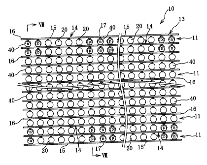
Fig. 8 is an equivalent circuit diagram of the solar cellassembly;
Fig. 9 is an enlarged sectional view of a plurality of spherical solar cells
and of the essential portions of a plurality of lead members;
Fig. 10 is an enlarged sectional view of plural bypass diodes and of the
essential portions of a plurality of lead members;
Fig. 11 is a plan view of a thin metallic sheet that is formed with a
plurality of openings;
Fig. 12 is a plan view of the thin metallic sheet after a plurality of
spots of electrically conductive paste have been applied to a plurality of
lead
strings and band portions;
Fig. 13 is a plan view of the thin metallic sheet after a plurality of
spherical solar cells and plural bypass diodes have been placed on a plurality
of spots of electrically conductive paste;
Fig. 14 is a plan view of the thin metallic sheet after spots of
electrically conductive paste have been applied to the summit portions of a
plurality of spherical solar cells and plural bypass diodes;
Fig. 15 is a plan view of a plurality of solar cell sub arrays that have
been made by dividing the thin metallic sheet into sections;
14
CA 02747540 2011-06-17
PCT/JP2008/003870
Fig. 16 is an elevation view of a solar cell assembly in matrix form
made by laminating and adhering together the plurality of solar cell sub
arrays;
Fig. 17 is a sectional view of a partially modified embodiment of the
solar cell module;
Fig. 18 is a sectional view of a partially modified embodiment of the
solar cell module;
Fig. 19 is an elevation view of a solar cell module according to a second
embodiment;
Fig. 20 is a sectional view taken along lines XX XX of Fig. 19;
Fig. 21 is a plan view of a thin metallic sheet that is formed with plural
slit shaped openings arranged in plural rows and plural columns;
Fig. 22 is a plan view of the thin metallic sheet after a plurality of
spherical solar cells and plural bypass diodes have been placed on a plurality
of spots of electrically conductive paste;
Fig. 23 is a plan view of the thin metallic sheet after spots of
electrically conductive paste have been applied to the summit portions of the
plurality of spherical solar cells and the plural bypass diodes;
Fig. 24 is a plan view of a plurality of solar cell sub arrays made by
dividing the thin metallic sheet into sections;
Fig. 25 is a side view of a cell assembly in matrix form in which a
plurality of solar cell arrays are laminated and adhered together;
Fig. 26 is an elevation view of a solar cell module according to a third
embodiment;
Fig. 27 is a sectional view taken along lines XXVII XXVII of Fig. 26;
Fig. 28 is an elevation view of a solar cell assembly;
CA 02747540 2011-06-17
PCT/JP2008/003870
Fig. 29 is a plan view of the solar cell assembly;
Fig. 30 is a bottom view of the solar cell assembly;
Fig. 31 is a sectional view taken along lines XXXI XXXI of Fig. 28;
Fig. 32 is an equivalent circuit diagram of the solar cell assembly;
Fig. 33 is an elevation view of the solar cell assemblyin a state in which
a plurality of solar cell arrays are connected in series;
Fig. 34 is an elevation view of the solar cell assembly in a state in
which a plurality of solar cell arrays are connected in parallel; and
Fig. 35 is an elevation view of a solar cell assembly in which the solar
cell group according to the third embodiment has been partially modified.
DESCRIPTION OF NUMERALS
[00261
1, 1A, 1B: solar cell modules
3, 4: panel members
6, 66: transparent synthetic resin
10, 10A, 10B, 10C: solar cell assembly
11, 11A, 11B, 11C: solar cell arrays
12, 12A: solar cell sub arrays
13, 13A, 13B: electrically conductive connecting mechanisms
14, 14B: lead members
15: lead string
16: lead piece
17: intermediate lead piece
20: spherical solar cell
21: p type spherical semiconductor
31: positive electrode
16
CA 02747540 2011-06-17
PCT/JP2008/003870
32: negative electrode
40: bypass diode
41: n type spherical semiconductor
47: anode
48: cathode
50, 50A: thin metallic sheets
63, 64: curved panel members
BEST MODE FOR IMPLEMENTING THE INVENTION
[00271
In the following, a best mode for implementing the present invention
will be explained on the basis of embodiments.
EMBODIMENT 1
[00281
First, the constitution of a solar cell module 1 will be explained.
As shown in Figs. 1 to 3, this solar cell module 1 is a module in the
form of a rectangular panel that, for example, is disposed in a vertical
attitude. The solar cell module 1 comprises a pair of panel members 3, 4 that
are formed as flat transparent plates, a solar cell assembly 10 made from a
plurality of solar cell arrays 11 that are sandwiched between the panel
members 3, 4, transparent synthetic resin 6 that is charged between the
panel members 3, 4, and a plurality of external leads 8p, 8n for outputting
the electric output of the plurality of spherical solar cells 20 to the
exterior.
With this solar cell module 1, the external leads 8p at the lower side are the
positive electrodes and the external leads 8n at the upper side are the
negative electrodes. It should be noted that up, down, left and right in Fig.
1
are explained as being up, down, left and right, and it is supposed that the
17
CA 02747540 2011-06-17
PCT/JP2008/003870
front side of the drawing paper is the incident side of sunlight.
[0029]
The panel members 3, 4 are provided in parallel for protecting both
sides of the plurality of solar cell arrays 11. The panel members 3, 4, for
example, may be made from any material selected from transparent glass,
transparent polycarbonate, acrylic, silicon resin, or the like. The gap
between
the panel members 3, 4 is set by a plurality of lead pieces 16 and a plurality
of intermediate lead pieces 17 that will be described later, which are
sandwiched and held between the panel members 3, 4. Among panel
members 3, 4, at least the panel member on the incident side of sunlight
should be made from a transparent material.
[0030]
The transparent synthetic resin 6 that seals the solar cell assemblylO
is charged between the panel members 3, 4. A material such as, for example,
EVA resin or silicon resin or the like is used as this transparent synthetic
resin 6. As shown in Figs. 17, 18, for the panel members 3, 4, it would also
be acceptable to provide a reflective layer 4a or a printed layer 4a that is
made to be ornamental on the inner surface of the panel member 4 on the
opposite side to the incident side of sunlight; or it would also be acceptable
to
provide a reflective layer 4b or a printed layer 4b that is made to be
ornamental on the outer surface of the panel member 4.
[0031]
As shown in Fig. 1, the end portions 8a of the plurality of external leads
8p at the lower end portion of the solar cell module 1 are each adhered by an
electrically conducting junction member 8b to the lower surface of a lead
piece 16 or of an intermediate lead piece 17 of a lead member 14 at the
18
CA 02747540 2011-06-17
PCT/JP2008/003870
lowermost edge of the cell assembly 10. Due to this, the external leads 8p at
the lower edge portion are electrically connected to the lead member 14 at
the lowermost edge of the cell assembly 10.
[0032]
And the end portions 8a of the plurality of external leads 8n at the
upper end portion of the solar cell module 1 are each adhered by an
electrically conducting junction member 8b to the upper surface of a lead
piece 16 or of an intermediate lead piece 17 of a lead member 14 at the
uppermost edge of the cell assembly 10. Due to this, the external leads 8n at
the upper edge portion are electrically connected to the lead member 14 at
the uppermost edge of the cell assembly 10.
[0033]
When manufacturing a large sized solar cell panel (module), a
constitution is adopted in which a plurality of modules similar to the above
module 1 are arranged in a plurality of rows and a plurality of columns, the
modules 1 that are vertically adjacent are electrically connected in series
together by connecting their external leads 8p, 8n, these plurality of modules
is attached to an external peripheral frame made from aluminum, and
electrical power is taken out from output terminals on this external
peripheral frame.
[0034]
Next, the solar cell assemblylO will be explained.
As shown in Figs. 4 to 8, the solar cell assembly 10 comprises: a plurality of
spherical solar cells 20 (corresponding to the "spherical semiconductor
elements") that are endowed with the function of photoelectric conversion
respectively, and that are arranged in the matrix form having a plurality of
19
CA 02747540 2011-06-17
PCT/JP2008/003870
rows and a plurality of columns, with their directions of electrical
conductivity being aligned along the column direction of the matrix; plural
bypass diodes 40 whose directions of electrical conductivity are arranged
along the column direction of the matrix and that are connected in inverse
parallel with the spherical solar cells 20; and an electrically conductive
connecting mechanism 13 in which the plural spherical solar cells 20 and the
plural bypass diodes 40 in each row are connected in parallel, while the
plurality of spherical solar cells 20 in each column and the plurality of
bypass diodes 40 for each column are connected in series respectively. The
cell assembly 10, which is built up from the plurality of solar cell arrays
11,
is made in the form of a flat plate. It should be understood that the
plurality
of spherical solar cells 20 and the plurality of bypass diodes 40 are arranged
in the matrix form having a plurality of rows and a plurality of columns.
[00351
The plurality of solar cell arrays 11 make up the solar cell assembly 10
, and each solar cell array 11 comprises a plurality of spherical solar cells
20
for that row, plural bypass diodes 40 for that row, and a pair of lead members
14, 14 that connect the plurality of spherical solar cells 20 and the plural
bypass diodes 40 in parallel . The electrically conductive directions of all
of
the pluralities of spherical solar cells 20 for the plurality of rows are all
aligned in the same direction (i.e. column direction). Solar cell arrays 11
that
are adjacent in the column direction of the matrix form share the lead
members 14 that are positioned between those solar cell arrays 11. The
pluralities of spherical solar cells 20 for each column and the pluralities of
bypass diodes 40 for each column are connected in series via the plurality of
lead members 14. At least a pair of bypass diodes 40 are included in each
CA 02747540 2011-06-17
PCT/JP2008/003870
solar cell array 11.
[00361
Next, the electrically conductive connecting mechanism 13 will be
explained. As shown in Figs. 4 to 7, the electrically conductive connecting
mechanism 13 includes a plurality of rectilinear lead members 14 that are
disposed at a plurality of positions between rows of the matrix and at both
end positions of the matrix in its column direction. Each of these lead
members 14 includes a pair of lead pieces 16 that are formed at both ends of
the lead member 14 and one or plural intermediate lead pieces 17 that are
formed at intermediate portions thereof, with the plural lead pieces 16, 17
having of a width larger than or equal to the diameter (i.e. the width) of the
bypass diode 40 respectively, and also includes plural lead strings 15 that
are formed between these lead pieces 16, 17 and having a width less than or
equal to the radius of the solar cell 20 respectively.
[00371
One or plural intermediate lead pieces 17 are provided at intermediate
portions of the lead member 4 along the row direction of the matrix. The lead
pieces 16 and the intermediate lead pieces 17 are disposed orthogonally to
the column direction of the matrix, and their width in the direction
orthogonal to the row direction of the matrix is preferably larger than the
diameter of the bypass diode 40. The lead members 14 are made from
metallic plate of, for example, iron nickel alloy (56% Fe, 42% Ni) having
thickness of 0.3 mm. The surfaces of the lead members 14 are plated with
silver or nickel. And the width of the lead strings is, for example, 0.5 mm to
0.7 mm. The width of the lead pieces 16 and of the intermediate lead pieces
17 may be, for example, 2.6 mm to 3.0 mm.
21
CA 02747540 2011-06-17
PCT/JP2008/003870
[0038]
Except for the lead member 14 at the uppermost edge of the cell
assembly 10, the positive electrodes 31 of the plurality of solar cells 20 are
adhered to the upper surface of each of the lead strings 15. And, except for
the lead member 14 at the lowermost edge of the cell assembly 10, the
negative electrodes 32 of the plurality of solar cells 20 are adhered to the
lower surface of each of the lead strings 15 with electrically conductive
adhesive material 19 (refer to Fig. 9). Thus, this electrically conductive
connecting mechanism 13 is made as a circuit connected in the form of a
mesh, in which the solar cells 20 are connected in series and also in
parallel.
[0039]
Moreover, except for the lead member 14 at the uppermost edge of the
cell assembly 10, the cathodes 48 of plural bypass diodes 40 are adhered to
the upper surfaces of the lead pieces 16 and of the intermediate lead pieces
17. And, except for the lead member 14 at the lowermost edge of the cell
group 10, the anodes 47 of the plurality of bypass diodes 40 are adhered to
the upper surfaces of the lead pieces 16 and of the intermediate lead pieces
17 with electrically conductive adhesive material 19 (refer to Fig. 10).
[0040]
The plurality of lead pieces 16 and the plurality of intermediate lead
pieces 17 of the cell assembly 10 described above are oriented in the
direction
orthogonal to the panel members 3, 4, and, since they are sandwiched and
held between the panel members 3, 4, accordingly the gap between the panel
members 3, 4 is set by the plurality of lead pieces 16 and the plurality of
intermediate lead pieces 17. Engagement portions 16a consisting of
semicircular notches are formed at the outer edge portions of the lead pieces
22
CA 02747540 2011-06-17
PCT/JP2008/003870
16, for engaging with and being guided by guide members of an automatic
assembly device while the solar cell sub arrays 12 are being laminated
together in a plurality of layers during assembly of the solar cell module 1,
as
will be described hereinafter.
[00411
Next, the construction of the spherical solar cells 20 will be explained.
As shown in Fig. 9, one solar cell 20 comprises: a spherical semiconductor 21
made from a p type semiconductor (a single silicon crystal); a flat surface 22
made by grinding a portion of the surface of the spherical semiconductor 21;
a pn+junction 25 in the form of a spot, made by forming an n+ diffused layer
24 as a spot on a portion of the outer layer of the spherical semiconductor 21
that is on the opposite side of the center of the spherical semiconductor 21
from the flat surface 22; a pn junction 27 in the form of a partially
spherical
surface, made by forming an n type diffusion layer 26 on a portion of the
outer layer of the spherical semiconductor 21; a pair of positive and negative
electrodes 31, 32 (corresponding to the "first conductive connection
portions")
attached to the pn+ junction 25 and to the pn junction 27 formed on parts of
the outer layer of the spherical conductor 21 on opposite sides relative to
its
center, i.e. at its both ends; and a reflection prevention layer 34 that is
formed over all portions except the positive and negative electrodes 31, 32.
The positive electrode 31 is electrically connected with low resistance to the
central portion of the flat surface 22 of the spherical semiconductor 21, and
the negative electrode 32 is electrically connected with low resistance to the
surface of the n type diffusion layer 26.
[00421
Since the positive and negative electrodes 31 and 32 are located in
23
CA 02747540 2011-06-17
PCT/JP2008/003870
symmetrical positions on opposite sides of the center of the spherical
semiconductor 21, and are made in the form of small spots, accordingly it is
possible for this spherical solar cell 20 to receive directly incident light
that
arrives at the surface of the spherical semiconductor 21, as well as reflected
light and diffused light, and accordingly its light utilization efficiency is
high.
And, since it is possible to connect the spherical solar cells 20 together
with
the lead members and the other electrically conductive members as a three
dimensional solid body, accordingly it is possible to provide a solar cell
module 1 whose freedom of design and design quality are outstanding.
[0043]
Next, a method for producing these spherical solar cells 20 will be
explained simply. First, a p type spherical silicon single crystal 21 is
prepared. For manufacturing this silicon single crystal 21, for example, after
silicon including a p type impurity has been melted in an upper melting pot,
drops of this molten silicon are allowed to fall freely. After these drops
have
been formed into spherical shapes by surface tension while falling, they are
cooled and solidified, so that they become spherical crystals. The various
conditions are set so that the diameter of these spherical crystals becomes
around 1.6 mm, and, since quite often small projections are formed on their
surfaces, accordingly finishing processing is performed so as to eliminate
these projections, thus producing spherical shapes of high dimensional
accuracy, for example of diameter around 1.5 mm.
[0044]
Next, a portion of this spherical silicon crystal 21 is processed by
grinding, so that the flat surface 22 of diameter 0.7 mm to 0.9 mm is
provided. This flat surface 22, along with preventing rolling of the spherical
24
CA 02747540 2011-06-17
PCT/JP2008/003870
crystal during subsequent manufacturing processing, is also used for
positioning when forming electrodes on it and connecting them with external
conductors, and so on. Next, heat is applied to the p type silicon single
crystal
21 in an atmosphere containing oxygen, so that its entire surface is covered
with a silicon oxide layer and thus a mask is formed against diffusion of
impurities .
[0045]
Next, the silicon oxide layer on the surface of the p type silicon single
crystal opposite to the flat surface 22 is eliminated by etching, so that
silicon
is exposed over a diameter of 0.7 mm to 0.9 mm. And next, phosphorus
diffusion is performed on the exposed surface of the silicon single crystal,
so
that a n+ type region 24 of depth 1 um is provided in the form of a spot, and
thereby a deep pn+ junction 25 is formed. Next, phosphorus diffusion is
performed again for a short time while omitting the flat surface 22 and the
silicon oxide layer on a portion around it, and thereby a new n type diffusion
layer 26 is provided on the greater portion of the spherical surface up to a
position around 0.3 um in depth, so that a shallow partially spherical pn
junction 27 is formed. And finally, a SiN layer is formed over the entire
spherical surface by a known CVD method, so that a reflection prevention
layer 34 is formed that also serves for passivation.
[0046]
Next, the construction of the spherical bypass diodes 40 will be
explained. As shown in Fig. 10, the bypass diode 40 comprises: a spherical
semiconductor 41 made from an n type semiconductor (a single silicon
crystal); a flat surface 42 made by grinding a portion of the surface of this
spherical semiconductor 41; a p+n junction 45 in the form of a partially
CA 02747540 2011-06-17
PCT/JP2008/003870
spherical surface, made by forming a p+ type diffusion layer 44 on a portion
of the outer layer of the spherical semiconductor 41; a pair of an anode 47
and a cathode 48 (corresponding to the "second electrically conductive
connection portions"), formed on the outer layer portion of the spherical
semiconductor 41 on opposite sides of its center, thus electrically connected
to both end of p+n junction 45 at its two ends; and a protective surface layer
49 that is formed over all portions except for the anode 47 and the cathode
48. The cathode 48 is connected with low resistance to the central portion of
the flat surface 42 of the spherical semiconductor 41, and the anode 47 is
connected with low resistance to the p+ type diffusion layer 44.
[0047]
These bypass diodes 40 are connected in inverse parallel to a plurality
of spherical solar cells 20 via the lead pieces 16 at both ends of each row of
the matrix, and via the plurality of intermediate lead pieces 17. These
bypass diodes 40 are spherical, and of similar size to the spherical solar
cells
20. Since it will be acceptable if, at least, bypass diodes 40 are provided at
the both end portions of each row, accordingly the bypass diodes that are
connected to the intermediate lead pieces 17 may be omitted, and, instead of
them, solar cells 20 may be provided.
[0048]
Next, a method for producing these spherical bypass diodes 40 will be
explained simply.
First, an n type spherical silicon single crystal 41 is prepared, having a
similar diameter to that of the spherical solar cell 20. And a flat surface 42
is
formed on a portion of this spherical n type silicon single crystal. Then, in
a
similar manner to that described above, an Si02 layer is provided as an
26
CA 02747540 2011-06-17
PCT/JP2008/003870
impurity diffusion mask on the surface of the lower hemispherical portion of
the n type silicon single crystal 41, centered around this flat surface 42.
Boron is then diffused into the remaining exposed surface of the n type
semiconductor 41, so that a p+ type region 44 is provided of depth around 10
lim. Due to this, a p+n junction 45 is formed. Furthermore, a surface layer of
Si3N4 is formed over the entire spherical surface in a similar manner to that
described above, so that a protective layer 49 is formed that also serves for
passivation.
[00491
This bypass diode 40 is endowed with the function of a rectification
diode, and is not required to generate any photoelectromotive force. For this
reason, it would also be possible to use a rectification diode having a planar
p
n junction, instead of the spherical bypass diode 40. However it is necessary
for it to be of a type having a characteristic in the forward direction at a
level
that, when a reverse voltage is applied by a solar cell with which it is
connected in inverse parallel, can bypass that current.
[00501
In this manner, , the solar cell 20 is electrically connected to the lead
strings 15 by the pair of the positive and negative electrodes 31 and 32 (the
first electrically conductive connection portions) that are formed in the
shape
of dots at the both ends of the spherical semiconductor 21 on the axial line
parallel to the column direction through its center and connected with low
resistance at the both ends of the pn+ junction 25 and the pn junction 27.
And, the bypass diode 40 is electrically connected to the lead pieces 16, 17
by
the pair of the anode 47 and the cathode 48 (the second electrically
conductive portions) that are formed on the axial line parallel to the column
27
CA 02747540 2011-06-17
PCT/JP2008/003870
direction through its center in the shape of dots at the both ends of the
bypass diode 40.
[0051]
Next, an equivalent circuit diagram for this solar cell module 1 will be
explained. Fig. 8 is an equivalent circuit diagram for a solar cell module 1
having a plurality of solar cells 20 and a plurality of bypass diodes 40
arranged in the matrix form having a plurality of rows and a plurality of
columns. An example will be explained of a case in which the plurality of
solar cells 20 provided to this solar cell module 1 are arranged in 15 rows
and
12 columns.
[0052]
If, for example, the open circuit voltage of a single solar cell 20 is 0.6 V,
then a voltage of 9.0 V will be generated, since 15 solar cells 20 are
connected
in series between the positive electrode 14p and the negative electrode 14n.
And, if the current generated by a single solar cell 20 is termed I, then a
current of 12-1 will be outputted from the positive electrode 14p to an
external circuit, since 12 of the solar cells 20 are connected in parallel.
In order to increase the output voltage of the module 1, the number of
solar cells 20 that are connected in series should be increased. And, in order
to increase the output current of the module 1, the number of solar cells 20
that are connected in parallel should be increased.
[0053]
Next, a manufacturing method for manufacturing this solar cell
module 1 will be explained on the basis of Figs. 11 to 16.
First, in a first process, a plurality of the spherical solar cells 20 are
prepared
in advance, each having a p type spherical semiconductor 21, a pn+ junction
28
CA 02747540 2011-06-17
PCT/JP2008/003870
25 made in spot form on a part of the outer layer of this spherical
semiconductor 21, a pn junction 27 like partially spherical surface, and a
reflection prevention layer 34. In parallel with this, a plurality of the
spherical bypass diodes 40 of similar size to the solar cells 20 are prepared
in
advance. It should be understood that, at this time, the solar cells 20 are in
their states before the positive and negative electrodes 31, 32 are connected
with low resistance to both ends of the pn+ junction 25 and the pn junction
27, and the bypass diodes 40 are in their states before the anodes 47 and
cathodes 48 are connected with low resistance to both ends of the pn
junctions 45.
[0054]
Next in a second process, as shown in Fig. 11, a plurality of openings
51 are made in the form of slits arranged in a plurality of rows and a
plurality of columns by performing a punching out process or an etching
process on a thin metallic sheet 50 of, for example, iron nickel alloy (of
thickness approximately 0.3 mm) whose surface is plated with silver or
nickel, so that a plurality of lead strings 15 each having a width less than
or
equal to the radius of the spherical solar cell 20 are formed between these
plurality of openings 51, with one or more wider band portions 52 that are
continuous along the column direction being formed at both end portions and
between adjacent columns along the row direction, and with yet wider band
portions 53 being formed at the upper edge portion and at the lower edge
portion.
[0055]
During punching out process or etching process, engagement portions
16a that consist of semicircular notches are formed on the external
29
CA 02747540 2011-06-17
PCT/JP2008/003870
peripheral portion, corresponding to the lead strings 15 of the band portions
52. These engagement portions 16a are used in subsequent processes for
forwarding the thin metallic sheet 50, and for positioning of a solar cell
array
11 that will be described later.
[0056]
Next, in a third process, as shown in Fig. 12, in order to connect a
plurality of the spherical solar cells 20 on each of the lead strings 15,
except
for the lead string 15 at the uppermost edge, an electrically conductive paste
in the semi solid state (this is a paste of Ag to which Al and glass frit have
been added, and corresponds to the "first conductive connection material") is
applied thereto in the form of a plurality of spots 31a.
[0057]
At the same time, in order to connect a plurality of the bypass diodes
40 at a plurality of sites on the band portions 52 corresponding to the
plurality of lead strings 15, except for the lead string 15 at the uppermost
edge, an electrically conductive paste in the semi solid state (this is a
paste of
Ag to which glass frit has been added, and corresponds to the "second
conductive connection material") is applied thereto in the form of a plurality
of spots 48a. The thickness at which these electrically conductive paste spots
31a, 48a is applied is around 0.3 mm to 0.5 mm.
[0058]
Next, in a fourth process, as shown in Fig. 13, the flat surfaces 22 of a
plurality of the solar cells 20 are connected respectively to each of the
plurality of spots 31a of electrically conductive paste that have been applied
on the lead strings 15. At the same time, the flat surfaces 42 of a plurality
of
the bypass diodes 40 are connected respectively to each of the plurality of
CA 02747540 2011-06-17
PCT/JP2008/003870
spots 48a of electrically conductive paste that have been applied on the band
portions 52.
[00591
Next, in a fifth process, as shown in Fig. 14, an electrically conductive
paste (this is a paste of Ag to which glass frit has been added, and
corresponds to the "first conductive connection material") is applied to the
summit portion of each of the plurality of solar cells 20, in the form of a
plurality of spots 32a. At the same time, an electrically conductive paste
(this
is a paste of Ag to which Al and glass frit has been added, and corresponds to
the "second conductive connection material") is applied to the summit
portion of each of the plurality of bypass diodes 40, in the form of a
plurality
of spots 47a. These spots 32a, 47a of electrically conductive paste that are
applied to the summit portions are of diameter about 0.5 mm and thickness
0.2 mm to 0.3 mm.
[00601
Next, in a sixth process, the thin metallic sheet 50 with the plurality
of solar cells 20 and the plurality of bypass diodes 40 thus arranged on it is
placed in an atmosphere of nitrogen gas at around 750 C, and thereby heat
is rapidly applied over a short time period, thus hardening the spots of
electrically conductive paste 31a, 32a, 47a, and 48a. At this time, the spots
31a, 32a of electrically conductive paste pierce through the reflection
prevention layers 34 of the solar cells 20, and are electrically connected at
low resistance to the surface of the semiconductor directly under them. In a
similar manner, the spots 47a, 48a of electrically conductive paste pierce
through the surface protective layers 49 of the bypass diodes 40, and are
connected at low resistance to the surface of the semiconductor directly
31
CA 02747540 2011-06-17
PCT/JP2008/003870
under them. By doing this, the positive and negative electrodes 31, 32 of the
solar cells 20 (i.e., the "first conductive connection portions") are formed,
and also the anodes 47 and cathodes 48 of the bypass diodes 40 (i.e., the
"second conductive connection portions") are formed.
[0061]
Next, in a seventh process, as shown in Fig. 15, the band portions 52 of
the thin metallic sheet 50 are made into the lead pieces 16 and the
intermediate lead pieces 17 by dividing them into sections by die punching or
with a laser beam, at intermediate positions corresponding to the openings
between the lead strings 15. Thus, a plurality of solar cell sub arrays 12 are
manufactured having the same shape and also the same dimensions,
including, for each row, a plurality of spherical solar cells 20, plural
bypass
diodes 40, plural lead strings 15, plural lead pieces 16, and one or plural
intermediate lead pieces 17.
[0062]
Next, in an eighth process, for each of these solar cell sub arrays 12, an
electrically conductive material 19 in paste form is applied to each of the
negative electrodes at the summit portions of the plurality of spherical solar
cells 20, and to each of the anodes 47 at the summit portions of the plural
bypass diodes 40.
[0063]
Next, in a ninth process, by the lead pieces 16 at both ends of the solar
cell sub arrays 12 being grasped by a pair of hands of an automatic assembly
device, and by the engagement portions 16a of the lead pieces 16 being
engaged to a pair of guide members of the automatic assembly device, the
plurality of solar cell sub arrays 12 are sequentially laminated together
32
CA 02747540 2011-06-17
PCT/JP2008/003870
while being guided and positioned via the pairs of lead pieces 16. Finally the
lead member 14 at the upper edge portion, on which no solar cells 20 or
bypass diodes 40 are provided, is laminated on to the assembly, and thereby
the plurality of spherical solar cells 20 and the plurality of bypass diodes
40
are assembled into a solar cell assemblylO in the matrix form having a
plurality of rows and a plurality of columns.
[0064]
Next, in a tenth process, as shown in Fig. 16, a weight W is mounted on
the upper edge of the cell assembly 10 in matrix form, and the electrically
conductive connection material 19 is hardened and the solar cell assembly 10
is manufactured by subjecting the cell assembly 10 to heating processing in
the state in which it is being compressed by the weight W in the column
direction. Thereafter, a plurality of external leads 8p, 8n are connected to
the
lead members 14 along the upper and the lower edge of the solar cell
assembly 10 by solder (the electrically conducting junction members) using a
laser beam.
[0065]
Next, in an eleventh process, in order to seal the solar cell assembly 10
between a pair of panel members 3, 4, it is disposed between the panel
members 3, 4 together with a transparent sheet of synthetic resin. Among
the panel members 3, 4, at least one of the panel members that is positioned
on the incident side of sunlight will be is made from a transparent material.
The panel members 3, 4 with this solar cell assembly 10 sandwiched between
them are loaded into the lower chamber of a predetermined laminator device
that has upper and lower containment chambers, and heat is applied with a
heater while vacuum exhausting these upper and lower chambers.
33
CA 02747540 2011-06-17
PCT/JP2008/003870
[0066]
After a fixed time period a gas is introduced into the upper chamber,
heat is applied at around 150 C while applying pressure to the panel
members 3, 4 on both sides due to the pressure difference between the upper
chamber and the lower chamber, and then the apparatus is returned to a
normal temperature. Due to this, the transparent synthetic resin sheet is
melted and hardened, so that the solar cell assembly 10 which is disposed
between the panel members 3, 4 is resin sealed with the transparent filler
material 6, along with the panel members 3, 4 on both sides being adhered
thereto. In this manner, it is possible to manufacture a single solar cell
module 1.
[0067]
Next, the advantages of the solar cell module 1 and its manufacturing
method of the present invention will be explained. According to this solar
cell module 1, the lead members 14 include one or plural lead strings 15
respectively to which the plurality of spherical solar cells 20 are
electrically
connected and that have width less than or equal to the radius of the
spherical solar cell 20, and the plurality of lead pieces 16, 17 that are
formed
integrally with the lead strings 15 at least at both end portions of the lead
members 14 and to which the bypass diodes 40 are electrically connected,
and that have width greater than or equal to the width of the bypass diodes
40. Therefore, when the solar cell sub array 12 is manufactured in which the
plurality of spherical solar cells 20 and the plural bypass diodes 40 are
attached to the single lead member that includes plural lead strings 15 and
plural lead pieces 16, 17, and when laminating together a plurality of these
soar cell sub arrays 12 in multiple layers, it is possible for the lead pieces
16
34
CA 02747540 2011-06-17
PCT/JP2008/003870
to be grasped by the hands of an automatic assembly device. Since it is also
possible to form engagement portions 16a or positional determination on the
lead pieces 16, for guiding the sub arrays 12 and determining their positions
during lamination, accordingly a solar cell module 1 can be assembled
efficiently by an automatic assembly device.
[00681
Moreover there is an advantage during the resin sealing process when
resin sealing the cell assembly 10 (i.e. the module main body portion) while
it
is sandwiched between panel members 3, 4, since it is possible to set the gap
between the pair of panel members 3, 4 by sandwiching the plurality of lead
pieces 16 and the plurality of intermediate lead pieces 17 between the pair of
panel members 3, 4.
[00691
Since the plurality of spherical solar cells 20 are installed, accordingly
the solar cell module 1 is capable of photoelectrically converting incident
light received in directions over a very wide range. Due to this, the light
utilization efficiency becomes greater, since it is possible to generate
electricity not only from light that is directly incident, but also from light
that is reflected and scattered internally to the solar cell module 1 and from
diffused light. If both of these flat shaped panel members 3, 4 are made from
a transparent material, then the solar cell module is produced that is capable
of generating electricity by receiving light from both sides.
[00701
Since, along with connecting the plurality of solar cells 20 in series and
also in parallel with the electrically conductive connecting mechanism 13
that is formed like a mesh and in which the plurality of lead strings 15 are
CA 02747540 2011-06-17
PCT/JP2008/003870
arranged in the form of a matrix having a plurality of rows and a plurality of
columns, also the bypass diodes 40 are connected in inverse parallel to the
plurality of solar cells 20 of each row, accordingly, even if this solar cell
module 1 is partially shielded from the sunlight and the output from some of
its solar cells 20 ceases, due to the bypass diodes 40, no hindrance is caused
to the output of the other spherical solar cells 20, and it is possible to
prevent
excessively great reverse voltage from being applied to some of the spherical
solar cells 20 that are shielded from the sunlight.
[0071]
Since it is possible to keep the amount of shielding of sunlight that is
directly incident on the solar cell module 1 small due to the lead strings 15
having width less than or equal to the radius of the spherical solar cell 20,
accordingly it is possible to enhance the efficiency of light utilization.
Since,
in the case of this solar cell module 1 that is formed as a flat plate, both
lighting and through vision are possible via the gaps between the solar cells
20, therefore, according to the density of the plurality of solar cells 20
with
respect to the module 1, free design becomes possible for selection of the
electricity generation capability, and for selection of the ratio between
illumination capability and light shielding capability. Moreover, it is
possible
to use this solar cell module 1 for a window material, i.e. as laminated glass
that is capable of generating electricity from sunlight, and furthermore it is
possible to reduce the overall material costs and the costs of installation
[0072]
Since, according to the manufacturing method for producing the solar
cell module 1 as described above, a plurality of the solar cell sub arrays 12
are manufactured, and these sub arrays 12 are sequentially laminated
36
CA 02747540 2011-06-17
PCT/JP2008/003870
together and are assembled into the cell assembly 10 in matrix form Hike a
panel, accordingly it becomes possible to sandwich those matrix form cell
assembly 10 between the panel members 3, 4 and to perform resin sealing
thereof. Due to this, it becomes possible to resin seal this cell assembly 10
between the pair of panel members 3, 4 without using any die having a
complicated construction. For this reason, it is possible to reduce the
manufacturing cost of the solar cell module 1, and it becomes possible to
increase the size of the solar cell module 1.
[0073]
Since the lead pieces 16 are integrally formed at both end portions of
the lead members 14, and thus, after having manufactured the plurality of
solar cell sub arrays 12, during lamination and assembly thereof, it is
possible for the lead pieces 16 to be grasped by the hands of an automatic
assembly device, and for positioning of the sub arrays 12 to be performed by
using the lead pieces 16, accordingly it is possible to assemble the solar
cell
module 1 efficiently and with good accuracy. And, during the process of resin
sealing the cell assembly 10, it is possible to set the gap between the pair
of
panel members 3, 4 by sandwiching the plurality of lead pieces 16, 17
between the pair of panel members 3, 4.
EMBODIMENT 2
[0074]
In this Embodiment #2, an example is shown of a solar cell module 1A
that is partially altered from that of Embodiment #1; thus, to elements that
are similar to ones of Embodiment #1, reference symbols that are the same
or similar are appended and explanation thereof is omitted, with only those
constitutions that are different from those of Embodiment #1 being
37
CA 02747540 2011-06-17
PCT/JP2008/003870
explained. This solar cell module 1A has a light reception surface that is
made in the form of a plurality of partially cylindrical surfaces, and is one
that can be applied as a solar cell module that also serves as a roof tile.
[0075]
As shown in Figs. 19, 20, this solar cell module 1A comprises: first and
second curved panel members 63, 64 that have a plurality of partially
cylindrical surfaces; a solar cell assembly 10A that is sandwiched between
the curved panel members 63, 64; transparent synthetic resin 66 charged
between the curved panel members 63, 64; and a plurality of external leads
68p, 68n for outputting the electric output of the plurality of spherical
solar
cells 20 to the exterior. Up, down, left and right in Fig. 19 are explained as
being up, down, left and right, and it is supposed that the front side of the
drawing paper in Fig. 19 is the incident side of sunlight.
[0076]
As shown in Fig. 20, the first curved panel member 63 closes over the
surface of the solar cell module 1A on the incident side of sunlight, and is
made from transparent material in a shape along a plurality of partially
cylindrical surfaces. And the second curved panel member 64 closes over the
surface of the solar cell module 1A on the side opposite to the incident side
of
sunlight, and moreover is made from transparent material in a shape along a
plurality of partially cylindrical surfaces.
[0077]
The gap between the curved panel members 63, 64 is set by a plurality
of lead pieces 76 and a plurality of intermediate lead pieces 77 being
sandwiched between the curved panel members 63, 64. A reflective layer
64a or a printed layer 64a on which ornamentation has been performed is
38
CA 02747540 2011-06-17
PCT/JP2008/003870
provided on the parts of the outer surfaces of the second panel member 64
that follow the partially cylindrical surfaces. And transparent synthetic
resin 66 is charged between the curved panel members 63, 64, thus sealing
the cell assembly 10A with resin.
[0078]
The end portions of the two external leads 68p at the lower edge of the
solar cell module 1A are each adhered with an electrically conductive
adhesive material to engagement portions 76a of the lead pieces 76 at the
two end portions of the lead member 74 at the lowermost edge of the cell
assembly 10A, and thus are electrically connected to the positive electrodes
31 of the plurality of solar cells 20 and to the cathodes 48 of the plurality
of
bypass diodes 40 on the lowermost edge of the matrix. And the end portions
of the two external leads 68n at the upper edge of the solar cell module 1A
are each adhered with an electrically conductive adhesive material to
engagement portions 76a of the lead pieces 76 at the two end portions of the
lead member 74 at the uppermost edge of the cell assembly 10A, and thus
are electrically connected to the negative electrodes 32 of the plurality of
solar cells 20 and to the anodes 47 of the plurality of bypass diodes 40 on
the
uppermost edge of the matrix.
[0079]
Next, the solar cell assembly 10A will be explained.
The solar cell assembly 10A comprises a plurality of spherical solar cells 20
that are arranged in the matrix form having a plurality of rows and a
plurality of columns, a plurality of bypass diodes 40 that are connected in
inverse parallel with these spherical solar cells 20, and an electrically
conductive connecting mechanism 13 for connecting these in parallel and
39
CA 02747540 2011-06-17
PCT/JP2008/003870
also in series. A plurality of solar cell arrays are made in the form of a
plurality of partially cylindrical surfaces (refer to Fig. 20) that extend
along
the row direction of the matrix connected at one or plural inflection points
dividing equally along rows of the matrix form. It would also be acceptable to
make the solar cell assembly in the form of two partially cylindrical surfaces
or a single partially cylindrical surface with no inflexion point.
[0080]
A plurality of solar cell arrays 11A constitute the solar cell assembly
10A. In each solar cell array 11A, in each pair of lead members 74, seven (for
example) solar cells 20 are arranged on each of a plurality of lead strings 75
that are formed as circular arcs, bypass diodes 40 are arranged on lead
pieces 76 at both ends of the lead member 74 and on each of the plurality of
intermediate lead pieces 77, and these are sandwiched between a pair of lead
members 74, 74. The directions of electrical conduction of all of the
spherical
solar cells 20 in the plurality of rows are all aligned in the same direction
(the column direction). Solar cell arrays 11A that are adjacent in the column
direction of the matrix share the lead members 74 that are positioned
between those solar cell arrays 11A. The pluralities of spherical solar cells
20
for each column and the pluralities of bypass diodes 40 for each column are
connected in series via the plurality of lead members 74.
[0081]
Next, the electrically conductive connecting mechanism 13A will be
explained. As shown in Fig. 19, the electrically conductive connecting
mechanism 13A is a connection circuit like a mesh in which, via the plurality
of lead members 74 that are disposed at a plurality of positions between the
rows of the matrix and at both ends of the matrix in the column direction, the
CA 02747540 2011-06-17
PCT/JP2008/003870
plurality of solar cells 20 and the plurality of bypass diodes 40 for each row
are connected in parallel, and the plurality of solar cells 20 in each of the
plurality of columns are connected in series and the plurality of bypass
diodes 40 in each of the plurality of columns are connected in series. Each of
these lead members 74 includes plural lead strings 75 that are shaped as
circular arcs and that have width less than or equal to the radius of the
spherical solar cells 75, wider lead pieces 76 at both end portions of the
lead
member 74, and a plurality of intermediate wider lead pieces 77 at inflexion
point.
[00821
Lead pieces 76 are formed integrally with the lead strings 75 at both
end portions of each of the lead members 74, and are disposed orthogonally
to the column direction of the matrix and have width in the direction
orthogonal to the row direction of the matrix greater than or equal to the
width of the bypass diodes 40. And, in each of the lead members 74,
intermediate lead pieces 77 are formed integrally with the lead strings 75 at
intermediate portions corresponding to plural inflexion points dividing
equally in the row direction of the matrix. Since the construction of each row
for connecting the plurality of solar cells 20, the plurality of bypass diodes
40, and the pair of lead members 74 are the same as the electrically
conductive connecting mechanism 13 of Embodiment #1, accordingly
explanation thereof will be omitted.
[00831
Next a manufacturing method for manufacturing the solar cell module
1A will be explained on the basis of Figs. 21 to 25; but explanation of
features
that are the same as ones of Embodiment #1 above will be omitted.
41
CA 02747540 2011-06-17
PCT/JP2008/003870
First, in a first process, a plurality of the spherical solar cells 20 and a
plurality of the bypass diodes 40 are prepared in advance, in a similar
manner to Embodiment #1. Next, in a second process, as shown in Fig. 21, by
performing a punching out process or an etching process on a thin metallic
sheet 50A similar to the one used in Embodiment #1, a plurality of openings
81 are provided in the form of slits arranged in a plurality of rows and a
plurality of columns. Along with the openings 81 in the shapes of circular
arcs being formed in the form of slits, a plurality of lead strings 75 for
each
column are made in the shape of circular arcs, and pluralities of band
portions 82, 83 and a plurality of engagement portions 76a formed on the
plurality of band portions 82 are also made.
[00841
Next, in a third process, a plurality of spots 31a (not shown in the
figures) of an electrically conductive paste for connecting a plurality of the
spherical solar cells 20, are applied on the lead strings 75, and also a
plurality of spots 48a (not shown ) of an electrically conductive paste for
connecting a plurality of the bypass diodes 40 are applied on the band
portions 82 that correspond to these lead strings 75. And next, in a fourth
process, as shown in Fig. 22, a plurality of solar cells 20 and a plurality of
bypass diodes 40 are connected to the plurality of spots 31a, 48a. Next, in a
fifth process, as shown in Fig. 23, electrically conductive paste is applied
to
the summits of the plurality of solar cells 20 and of the plurality of bypass
diodes 40 in the form of spots 32a, 47a respectively.
[00851
Next, in a sixth process, heat is rapidly applied to the thin metallic
sheet 50A and the spots 31a, 32a, 47a, 48a are hardened. And next, in a
42
CA 02747540 2011-06-17
PCT/JP2008/003870
seventh process, as shown in Fig. 24, the plurality of band portions 82 on the
thin metallic sheet 50A are divided into sections by a punching out process or
with laser light, so that lead pieces 76 and intermediate lead pieces 77 are
formed, and thereby a plurality of solar cell sub arrays 12A having the same
shape and the same dimensions are manufactured. Next, in an eighth
process, in each of the solar cell sub arrays 12A, electrically conductive
connection material 19 is applied to each of the negative electrodes at the
summit portions of the plurality of spherical solar cells 20 and to each of
the
anodes 47 at the summit portions of the plurality of bypass diodes 40. And
next, in a ninth process, as shown in Fig. 25, the plurality of solar cell sub
arrays 12A are sequentially laminated together, so that the plurality of
spherical solar cells 20 and the plurality of bypass diodes 40 are assembled
into a solar cell assembly 10A in the form of a matrix having a plurality of
rows and a plurality of columns.
[00861
Next, in a tenth process, the finished solar cell assembly 10A is formed
by subjecting this cell assembly 10A to heating processing and by thus
hardening the electrically conductive adhesive material 19. Thereafter,
external leads 68p, 68n are soldered by a laser beam to the engagement
portions 76a of the lead pieces 76 at the top edge and at the bottom edge in
the column direction of the solar cell assembly 10A. And next, in an eleventh
process, the solar cell assembly 10A in the form of a matrix is positioned
between a pair of curved panel members 63, 64, transparent synthetic resin
66 is charged between the curved panel members 63, 64 via a transparent
synthetic resin sheet and is thereafter subjected to heating processing, and
thereby the solar cell module 1A is manufactured.
43
CA 02747540 2011-06-17
PCT/JP2008/003870
[0087]
Next, the operation and the advantages of the solar cell module 1A and
of the manufacturing method thereof will be explained.
Since, according to this solar cell module 1A, the light reception surfaces of
the curved panel members 63, 64 are formed in the shape of a plurality of
partially cylindrical surfaces, as contrasted with the panel members 3, 4 of
Embodiment #1 described above which are formed as flat plates, accordingly
the light reception surface is increased, and moreover it is possible to
suppress fluctuations of the electric output of the solar cell module 1A, even
if the direction of directly incident solar radiation changes along with the
passage of time. A solar cell module 1A having surfaces of this type shaped
as partial cylinders can be applied as a roof tile or as a wall material.
Thus, it
is possible to endow a solar cell module 1A of which the light reception
surface is formed as partial cylinders with good freedom of design
(designability).
[0088]
As the reflective layer 64a, for example, it would also be acceptable to
arrange to employ a thin layer made from metal whose reflectivity is high, or
to employ a method of applying white colored ceramic paint by silk screen
printing and then heat firing the result. It would also be acceptable to print
ceramic paint having a desired color or design pattern, although the
reflectivity would be reduced to a certain extent. In this case, apart from
light that is reflected from and scattered by the reflective layer being
received by the solar cells and thus increasing their photoelectric output,
application is also possible as a solar cell panel of a type integrated with a
building material in which an attractive design is incorporated, and which
44
CA 02747540 2011-06-17
PCT/JP2008/003870
controls the visibility, the solar radiation, and the heat to be moderate . It
should be understood that it would also be acceptable to apply this type of
reflective layer to Embodiment #1 described above. Explanation of other
features of the operation of this embodiment and of other benefits thereof
will be omitted, since they are the same as those of Embodiment #1.
EMBODIMENT 3
[00891
In this Embodiment #3, an example is shown of a solar cell module 1B
that is partially altered from that of Embodiment #1; thus, to elements that
are similar to ones of said Embodiment #1, reference symbols that are the
same or similar are appended and explanation thereof is omitted, with only
those constitutions that are different from those of Embodiment #1 being
explained. This solar cell module 1B in one in which, by wiring up a plurality
of lead terminals 81a, 81b that are provided on the exterior of the module 1B
to external connection leads as desired, it is possible to set the voltage and
the electric current outputted from the module 1B freely.
[00901
As shown in Figs. 26, 27, this solar cell module 1B comprises a pair of
panel members 3, 4 that are formed as flat plates, a solar cell assembly 10B
sandwiched between the panel members 3, 4, transparent synthetic resin 6
charged between the panel members 3, 4, and a plurality of external leads
8p, 8n for outputting the electric output of a plurality of spherical solar
cells
20 to the exterior. Up, down, left and right in Fig. 26 are explained as being
up, down, left and right, and it is supposed that the front side of the
drawing
paper in Fig. 26 is the incident side of sunlight.
[00911
CA 02747540 2011-06-17
PCT/JP2008/003870
The pair of panel members 3, 4 are provided in parallel, in order to
close both sides of a plurality of solar cell arrays 11B. The gap between the
panel members 3, 4 is set by a plurality of lead pieces 16 and a plurality of
intermediate lead pieces 17 that are sandwiched between the panel members
3, 4. The transparent synthetic resin 6 is charged between the panel
members 3, 4 in order to seal the solar cell assembly 10B with resin, and at
least the panel member 3 on the incident side of sunlight is made from a
transparent material. A plurality of pairs of lead terminals 81a, 81b that
will
be described later are provided on the left and right side edge portions of
the
module 1.
[0092]
Next, the solar cell group 10B will be explained.
As shown in Figs. 28 to 32, the cell assembly 10B comprises: a plurality of
spherical solar cells 20 that are endowed with the function of photoelectric
conversion, and that are arranged in the matrix form having a plurality of
rows and a plurality of columns, with their directions of electrical
conductivity being aligned along the column direction of the matrix; a
plurality of bypass diodes 40 arranged in a plurality of columns at both end
portions of rows of the matrix and at intermediate portions thereof, and an
electrically conductive connecting mechanism 13B in which the plurality of
spherical solar cells 20 in each row are connected in parallel. At least one
column of bypass diodes 40 may be provided.
[0093]
Each of the plurality of solar cell arrays 11B that make up the cell
assembly 10B comprises a plurality of spherical solar cells 20 and plural
bypass diodes 40 for that row, and the plurality of solar cell arrays 11B are
46
CA 02747540 2011-06-17
PCT/JP2008/003870
sandwiched between a pair of lead members 14B, 14B. The electrically
conductive directions of all of the pluralities of spherical solar cells 20
for the
plurality of rows are all aligned in the same direction (i.e.column
direction).
The cell assembly 10B is made by laminating a plurality of spacers 85 made
from insulating material between solar cell arrays 11B that are adjacent in
the column direction of the matrix. The spherical solar cells 20 are similar
to
the solar cells 20 of Embodiment #1 described above. It should be understood
that it is not necessary to provide a plurality of the spacers 85 for each
row; it
would also be acceptable to provide only one.
[0094]
Next, the electrically conductive connecting mechanism 13B will be
explained. This electrically conductive connecting mechanism 13B is a
mechanism that connects in parallel the plurality of cells 20 and the
plurality of bypass diodes 40 in each row via a pair of lead members 14B,
14B; the lead members 14B comprise a plurality of lead strings 15, a
plurality of lead pieces 16, and one or plural intermediate lead pieces 17,
and are similar to the lead members 14 of Embodiment #1. However, lead
terminals 81a, 81b (external leads) are provided to the lead pieces 16,
extending to the exterior in the row direction. It would be acceptable to form
a lead terminal 81a or a lead terminal 81b integrally at least at the one end
portions of the lead members 14B. The connection mechanism between the
plurality of solar cells 20, the plurality of bypass diodes 40, and the pair
of
lead members 14b for each row is the same as the electrically conductive
connecting mechanism 13 of Embodiment #1, and accordingly explanation
thereof is omitted.
[0095]
47
CA 02747540 2011-06-17
PCT/JP2008/003870
Next, the operation of this solar cell module 1B and the advantages
thereof will be explained. With this solar cell module 1B, the output
characteristics of the module can be varied as appropriate by altering the
connection mechanism of the plurality of lead terminals 81a, 81b by
changing over external switches. If the maximum output voltage is to be
extracted from the solar cell module 1B, then, as shown in Fig. 33, the arrays
11B in the plurality of rows may be connected in series via external leads 82.
On the other hand, if the maximum output current is to be extracted, then,
as shown in Fig. 34, the arrays 11B in the plurality of rows may be connected
in parallel via external leads 83 and 84.
[0096]
While, in the examples described above, examples were explained in
which the plurality of solar cell arrays 11B were connected in series or were
connected in parallel, it would also be possible to set the number of the
solar
cell arrays 11B that are connected in series appropriately in order to match
the desired output voltage, and to set the number of the solar cell arrays 11B
that are connected in parallel appropriately in order to match the desired
output current. Explanation of other features of the operation of this
embodiment and of other benefits thereof will be omitted, since they are
generally the same as those of Embodiment #1.
[0097]
It would also be possible to apply the following variant embodiments to
the solar cellassembly 10B described above.
As shown in Fig. 35, in a solar cell assembly 10C, the solar cell arrays 11B
and solar cell arrays 11C, in which the electrically conductive directions of
the spherical solar cells 20 and the bypass diodes 40 of the solar cell arrays
48
CA 02747540 2011-06-17
PCT/JP2008/003870
11B are inverted, are arranged alternately with a plurality of spacers 85
made from insulating material being sandwiched between them. Since the
arrays 11B, 11C are independent, it is thus possible to employ a
configuration in which the plurality of arrays 11B are inverted, as described
above, in consideration of convenience in wiring the lead terminals 81a, 81b.
to the exterior. It is also possible to set the gaps between the arrays 11B,
11C
freely, by varying the sizes of the spacers 85 and/or by omitting the spacers
85.
[0098]
Now, examples in which these embodiments are partially modified will
be explained.
[1] The ratio of lighting versus output electrical power provided by these
modules 1, 1A, and 1B principally depends on the output electrical power of
the plurality of solar cells 20 that are employed, versus the total area
shielded from light by the solar cells 20, the bypass diodes 40, and the
electrically conductive connecting mechanism 13. It is possible, by varying
the gaps between the solar cells and between the solar cell arrays for this
reason, appropriately to design the arrangement of the plurality of spherical
solar cells 20 that are used and the number thereof that are used, and the
shape and so on of the electrically conductive connecting mechanism 13, in
order to increase the freedom of design and to enhance the added value
during use as a window material.
[0099]
[2] It would also be possible to use spherical solar cells and bypass diodes
in
which the n type layers and the p type layers of the spherical solar cells 20
and the bypass diodes 40 of the above modules 1, 1A, and 1B are inverted. In
49
CA 02747540 2011-06-17
PCT/JP2008/003870
this case, the output of the module would be reversed.
[3] Apart from the above, for a person skilled in the art, it would be
possible
to implement alterations to the above embodiments in various other ways ,
provided that the distinguishing characteristics of the present invention are
not deviated from; so that the present invention is to be understood as also
including those variant embodiments.
INDUSTRIAL APPLICABILITY
[0100]
In addition to the above described solar cell panels or modules, the solar
cell module of the present invention could also be applied to various
structural materials such as, for example, a window material, a glass
window, an atrium, a top light, a curtain wall, a facade, a canopy, a louver,
a
double skin outer surface, a guard rail of a balcony, or a soundproofing wall
of a high speed road or a railroad or the like.