Note: Descriptions are shown in the official language in which they were submitted.
CA 02748369 2011-06-27
WO 2010/080736 PCT/US2010/020061
WIRELESS CHARGING SYSTEM WITH DEVICE POWER COMPLIANCE
BACKGROUND OF THE INVENTION
This application is related to U.S. Application No. 12/349,355, entitled
"Metered
Delivery of Wireless Power" filed January 6, 2009, now U.S. Patent No. , which
is
incorporated by reference.
The present invention relates to wireless power systems and more particularly
to
such systems capable of powering multiple devices simultaneously.
Wireless power or charging systems are well known and widely used. Such
systems typically include a primary power supply and one or more secondary
devices. The
primary inductively powers the secondary devices when they are brought into
proximity with the
primary.
While such systems are well known, a number of potential problems are
associated with such systems.
First, each primary supply is typically sized for a particular application
depending
upon the power to be drawn from the power supply. Issues arise when the power
requirements
of the secondary devices are greater than the power capacity of the primary
supply. The
secondary device may shut down, or the secondary device may attempt to charge
at the reduced
power level available which may not be appropriate for the device. Typically
either result
happens without feedback or warning to the user. Consequently, the device may
be charged
improperly or not at all.
1
CA 02748369 2011-06-27
WO 2010/080736 PCT/US2010/020061
Second, multiple power supplies typically are required for multiple secondary
devices - i.e. one for each device. This can result in a multitude of power
supplies, which are
expensive and difficult to store, use, and match with the secondary devices.
SUMMARY OF THE INVENTION
The aforementioned problems are overcome in the present invention in which the
various components within the wireless power system communicate power
requirements and
capabilities to one another so that power compliance can be managed. More
specifically, each
secondary device can communicate with the wireless power supply to provide an
indication of
the power requirements of each device; and conversely, the power supply can
communicate with
each secondary device to provide an indication of the power capacity of the
supply.
A wireless power control can then solve for power distribution requirements
among the power supply and the secondary units. The control can provide an
alert if the power
requirement of the secondary device exceeds the system capacity. The control
also enables
charging at a reduced power level. If multiple secondary devices are brought
into the charging
system, the control can distribute power among the devices.
Consequently, the present invention provides enhanced power compliance within
a wireless charging system. The system provides an indication of mismatches
between power
capacity and power requirements and also provides power distribution among
multiple devices to
enable multiple devices to be charged using a single power supply.
These and other objects, advantages, and features of the invention will be
more
fully understood and appreciated by reference to the description of the
current embodiments and
the drawings.
2
CA 02748369 2011-06-27
WO 2010/080736 PCT/US2010/020061
BRIEF DESCRIPTION OF THE DRAWINGS
Fig. 1 is a schematic illustration of a prior art wireless power or charging
system;
Fig. 1.5 is a state diagram for the wireless power control;
Fig. 2 is a schematic illustration of a wireless charging system constructed
in
accordance with a first embodiment of the invention;
Fig. 3 is a schematic illustration of the power supply side of the wireless
charging
system;
Fig. 4 is a schematic illustration of the wireless charging system in which
the third
wire communicates analog data;
Fig. 4.5 is a schematic illustration of the wireless charging system showing
the
communications used to communicate information between the primary and the
secondary;
Fig. 4.6 is a schematic illustration showing a first alternate embodiment of
the
power supply;
Fig. 4.7 is a schematic illustration of a second alternate embodiment of the
primary;
Fig. 4.8 is a schematic illustration of a third alternate embodiment of the
wireless
charging system;
Figs. 4.85, 4.86, and 4.87 are schematic illustrations of power accounting and
communications protocols;
Fig. 4.9 is a schematic illustration of another alternative embodiment of the
primary;
3
CA 02748369 2011-06-27
WO 2010/080736 PCT/US2010/020061
Fig. 5 is a schematic illustration showing how the power is reconciled by the
wireless power supply;
Fig. 6 is a schematic illustration of a power distribution system using the
placement of devices as the priority of the charging sequence;
Fig. 7 is a schematic illustration of a power distribution system managing
power
distribution by understanding power ratios from each device;
Fig. 8 shows an example of the analog output table to select the wattage of
the
power supply;
Fig. 9 is a data sequence between the primary source A and the secondary
device
B;
Fig. 10 shows a basic feedback mechanism that can be understood by touch or
sound;
Fig. 11 shows a placement sequence table that provides outcomes and events;
Fig. 12 is a schematic illustration of a fifth alternate embodiment of the
primary
providing a four-unit charger;
Fig. 13 shows how additional capacity can be added to the primary of Fig. 12;
and
Fig. 14 is a schematic illustration of the wireless charging system providing
further improved control, regulation, and anticipation of power fluctuations.
DESCRIPTION OF THE CURRENT EMBODIMENTS
A prior art wireless charging system 10 is illustrated in Fig. 1 and includes
a
wireless power supply (WPS) 12 and a portable secondary device 14. The
wireless power supply
12 in turn includes a rectifier 16, a DC/DC converter 18, an inverter 20, a
capacitor 22, an
4
CA 02748369 2011-06-27
WO 2010/080736 PCT/US2010/020061
inductive coil 24, and a control 26. The portable device 14 includes a
secondary coil 30, a
capacitor 32, a rectifier 34, a DC/DC converter 36, and a load 38. When the
secondary coil 30 is
brought into proximity to the primary coil 24, and when the primary coil is
powered, an
inductive link is established; and a voltage is induced in the secondary coil.
The wireless
charging system 10 as thus far described is well known and its structure and
function need not be
further described in detail.
Power systems such as that illustrated in Fig. 1 typically require the user to
understand and remember what devices and what power supplies work together.
Two different
power supplies with different power capacities, but also with the same
connector, can physically
connect to the same device. However, use of the incorrect supply with a device
can potentially
cause failure or improper operation. The user becomes aware of such failure or
improper
operation only through some type of failure mode, such as over-powering of the
device or failure
to charge the device.
The present invention enables the power systems and the secondary devices to
communicate with each other and to be configurable and to manage power
compliance among
the various components of the system.
In the past power systems have been dependant on the user to know and
understand what devices and power supplies work together. Two different power
supplies with
the same connector can easily connect to the same device. This can potentially
cause failure or
improper operation. The user knows this only by the failure mode.
This invention seeks to solve this issue by allowing power systems to
communicate and be configurable. Devices can communicate with power supplies
and supplies
with devices all communicating to the user.
CA 02748369 2011-06-27
WO 2010/080736 PCT/US2010/020061
Power supply compliance
The power supply and wireless power supply both communicate capacity
respectively and can solve for power distribution requirements. The
information from remote
power supplies or internal power supplies is communicated to the wireless
power control. The
system is designed to alert the user by way of primary to secondary
communications that the
device requires more power than the wireless power supply and the main power
supply are
capable of supplying.
Primary to secondary communications
There are multiple ways to communicate information from the primary to the
secondary, for example, as disclosed in this application. Some methods involve
small variances
- around 1% to 2% of the power to modulate a simple signal. Other methods stop
oscillation
completely for short periods to send very basic signals. These basic
communications enable the
following features:
Primary request for an authorization to charge - billing
Authentication for proper charge - authentication handshake
Not enough power available for this device - less than wattage required
available
Communications of sequence for charge - next to charge - 2n' in line for a
charge
Configuration of a device - mute, vibrate, radio off
Non compliance with the standard
Smaller power supplies charging multiple devices
As one example, the present invention enables a single five-watt power supply
to
charge several five-watt devices in sequence. Each device communicates charge
ratio (power in
vs. power used over time) and need for charge (present capacity). Using these
ratios from each
6
CA 02748369 2011-06-27
WO 2010/080736 PCT/US2010/020061
device, the charge can be split and sequenced allowing many devices to have
proper power with
a very limited charge. This approach is like passing the charge cable around
the table as needed,
but doing so only wirelessly. One exemplary use is a conference table with
several laptops.
Only one laptop really needs to be charged at a time. The sequencing
eliminates the need for
having the ability to cover the wattage of all the devices at maximum power
and lowers the cost
of implementation.
Wireless power enhancement utilizing power management interface
The wireless power supply includes the power management unit. In prior art
systems include backlighting, radios, hard drives, GSM pulses, and the like
that are turned on
and off, the power supply is designed to react to these systems and provide
stable power. The
present invention uses knowledge from the system when aspects of the system
that require power
are being turned on and off to efficiently manage the control by anticipating
a percentage of
change based on the power impact. This knowledge allows the power supply to
react directly to
the need. In prior art systems, a proportional-integral-derivative (PID)
control loop saves time
by eliminating multiple passes of the loop; and the system can respond more
quickly. By
connecting the power management unit (PMU) of the secondary device and
assigning error
values for each load, the sum of the change in load can be easily transferred
from the power
management unit to the secondary wireless power control and then communicated
to the wireless
power supply to improve loop reaction time.
General control description
The error-based control mode allows for a control loop configuration between
the
secondary control interface (SCI) and primary control interface (PCI). The PCI
responds to the
control error feedback packet from the SCI to determine the adjustment needed
to reach the
7
CA 02748369 2011-06-27
WO 2010/080736 PCT/US2010/020061
operating point. This provides for significant design freedom. A variety of
types of control can
be implemented on the secondary side. Examples of algorithms include constant
current,
constant voltage, or constant power. The state diagram in Fig. 1.5 sets forth
the algorithm used
in this control method.
Predictive PID Control
The PID system error and timing can be coordinated between the wireless power
primary control and the secondary receiver and the power management systems.
Table 1 shows
how this timing and power can be used to formulate the additional required
power that will be
required and the minimum timing used to coordinate these systems. Arbitrary
current and timing
are shown as an example. These values can be pre-measured for best overall
system
performance and stored in the secondary system for coordination with the power
management
system.
Power Management Table Portable Device
Power System Power System System
Enabled Delta
Main Processor 200ma
LCD Backlight 200ma X
GSM Radio 300ma X 550mA
Bluetooth Radio 50ma X
Commmunications 25ma
Camera LED 80ma
Table 1. Power management table for a portable device showing the control
values used when
the LCD, GSM and Bluetooth need to be enabled.
The Coil_Current_Setpoint is then calculated using the measured value plus the
sum of the new control value as a sum of Table 1. This allows the system to
have much faster
8
CA 02748369 2011-06-27
WO 2010/080736 PCT/US2010/020061
control by limiting the number of loops required for course control. This
coarse control allows
less ripple by limiting the time required for the PID to respond as this
allows predictive and
reactive input.
Timing of Control
Time
0 10 20 30 40 50 60
Priority PID Command
LCD Backlight
GSM Radio
Bluetooth Radio
Table 2. Timing of control for primary and secondary side power management
coordination. It
should be noted latency of power control for each system may be considered for
control.
PID Control
The control algorithm uses a PID method of control. The PID control algorithm
is
not run continuously, as this is more likely to result in corrupted data
communication. Instead,
the PID algorithm attempts to change the primary coil current to a calculated
operating point
between the reception of control feedback packets (CFP).
The SCI preferably does not attempt communication during the time in which the
PID algorithm is active. The minimum timing between control error feedback
packets is defined
within the Device ID payload.
A generic PID controller is represented in Table 3. This math is recreated
within
the PCI.
9
CA 02748369 2011-06-27
WO 2010/080736 PCT/US2010/020061
........................................
........................................
........................................
........................................
........................................
........................................
........................................
........................................
........................................
D--
0
Utput
........................................
Error
Table 3. Generic PID Controller
New Coil Current Calculation
The PCI coil current signal used by the PID control loop is sampled by the A/D
and a rolling average is calculated. The algorithm calculates a new target PCI
coil current each
time a non-zero control error feedback packet is received from the SCI using
the following
equation:
(Previous_Setpoint * Max_Error_Counts)
Coil_Current_Setpoint = (2)
(Feedback_Error + Max_Error_Counts)
The "Feedback_Error" is defined as the payload of the control error packet
transmitted by the SCI:
Feedback Error = Reactive Error + Predictive Error
If the Feedback_Error is zero, the PID control loop is not run, because no
adjustment to the
operating point is necessary.
CA 02748369 2011-06-27
WO 2010/080736 PCT/US2010/020061
The "Previous_Setpoint" is defined as the most recent stabilized primary coil
current for the initial run of the PID loop, or the last stabilized primary
coil current following an
adjustment.
The "Max_Error_Counts" is defined as the maximum error that can be reported
by the SCI. In the current embodiment, this is within a range of +/-127.
The coil current returns to a steady state prior to activating the PID so that
error
calculations are accurate and the required number of frequency adjustments is
minimized. The
algorithm waits for the coil current to stabilize following the reception of a
data packet from the
SCI, determined by the "PID Delay Time" parameter. The correct delay period is
based upon the
maximum amount of time required for the PCI coil current to return to its
steady state following
data communications and the filter delays of the feedback signal to the
primary A/D.
The following calculation is made to achieve the new operating point:
Calculated_Error = Previous_Setpoint - Coil_Current_Setpoint (2)
Proportional Calculation
The proportional term of the algorithm is calculated in the equation below.
P Proportional-Term = Calculated-Error *K (3)
Integral Calculation
The integral term of the algorithm is calculated in the equation below.
Integral Term = Calculated Error * K + Previous-Integral-Term (5)
Integral Update_Interval
Where Integral Update Interval is a gain adjustment based on the desired
integration rate. Wind-
up is controlled using the Integral Upper Limit and Integral Lower Limit
parameters.
11
CA 02748369 2011-06-27
WO 2010/080736 PCT/US2010/020061
Derivative Calculation
The derivative term of the algorithm is calculated in the equation below.
Derivative_Term (Calculated Error Previous _Calculated _Error) *K
= (6)
Derivative-Update-Interval
Where Derivative Update Interval is a gain adjustment based on the desired
differentiation rate.
Total PID Calculation
The total PID calculation is the sum of the proportional, integral, and
derivative
terms.
PID_Output = Proportional_Term + Integral-Term + Derivative-Term (6)
Maximum output is controlled using the PID Output Upper Limit and PID Output
Lower Limit
parameters.
Updated Operational Point Calculation
The final frequency adjustment is calculated in the equation below.
Frequency_Output = Frequency_Output + (PID_Output * GainCorrection_Factor) (7)
PID_Scale_Factor
The "Gain_Correction_Factor" divides the resonance curve into piecewise linear
functions.
The "PID_Scale_Factor" is used to help with the integer math in the PID
calculations.
Once the "PID Delay Time" has expired, the PID loop actively attempts to bring
the PCI coil current to the new target set-point using the equations above
during the "PID Active
Time".
12
CA 02748369 2011-06-27
WO 2010/080736 PCT/US2010/020061
Finally, the PID control is inhibited during the "PID Settle Time" so that an
accurate reading of PCI coil current can be recorded by the primary and an
accurate reading of
voltage or current by the SCI.
Error Based Control Loop Timing
The maximum allotted time between adjustments of the primary coil frequency
during the PID Active Time for the Error Based Control loop is 4 milliseconds
(ms). This
control loop is coordinated with the power management system and control
timing for powering
systems. The error and communications are communicated in conjunction with the
power
management system and timing control. Timing is controlled and coordinated by
the primary
wireless power supply using the Power and Control Latency value from the
table. The primary
and secondary systems coordinate the timing based on the value shared by the
maximum value
of the sum of the power delta being manipulated.
The current embodiment is one way to use the error control, and one skilled in
the
art will recognize that the described methodology can be used in many ways to
coordinate
wireless power control and device power management.
Fig. 2 shows a system where the power supply, the wireless power supply, and
the
secondary device all reconcile power to the device. The cable 218 provides a
hard-wired
connection between the power supply 212 and the wireless power supply 214. The
wireless
power supply 214 and the wireless power device 216 are inductively coupled as
in the prior art.
The wattage of the DC power supply 212 is communicated by way of an analog
voltage, a digital signal, or a frequency modulation to the wireless power
supply 214. The
wireless power supply includes a control 220 and indicators 222. The wireless
power supply 214
13
CA 02748369 2011-06-27
WO 2010/080736 PCT/US2010/020061
receives power capacity information from the power supply 212 and device power
requirements
from the secondary device 216.
The secondary 216 includes a secondary device control 224 and indicators 226.
The secondary device 216 receives system power capacity information from the
wireless power
supply 214 and can charge or indicate incompatibility in response to that
information.
It is possible that the power supply 212 has a lower voltage and/or power
capacity
than the wireless power supply 214. In such case, the wireless power control
220 configures
itself so that it is capable of supplying only the power received from the
power supply 212.
It also is possible that the voltage and/or power capacity of the power supply
214
is less than the voltage or power requirement of the secondary device 216. In
such case, an error
signal is indicated on the indicators 222 and/or 226. Additionally, the
secondary device control
224 can make a decision regarding whether to not charge at all or whether to
charge at the
reduced available power level. In response to the decision of the device
control 224, the wireless
power control 220 can configure itself to not provide power at all or to
provide power at the level
requested by the secondary device control 224.
Accordingly, the system 210 of Fig. 2 enables 1) power compliance between the
secondary device 216 and the wireless power supply 214, 2) communications
between the
secondary device 216 and the wireless power supply 214, 3) smaller wireless
power supplies for
charging multiple devices, and 4) use of the device's PMU.
Fig. 3 shows how the power supply uses the third wire to communicate the power
available from the power supply 312 to the wireless power supply 314. This
configuration uses a
data signal to communicate the power data to the wireless power supply 314.
The third wire 319
14
CA 02748369 2011-06-27
WO 2010/080736 PCT/US2010/020061
directly connects the power control circuit 328 of the power supply 312 with
the drive control
324 of the wireless power supply 314.
Fig. 4 shows the third wire 419 communicating analog data that represents the
power available from the power supply 412. Accordingly, the system 410 in Fig.
4 is an analog
implementation of the system 310 illustrated in Fig. 3. As in previous
embodiments, the wattage
is communicated by way of the analog voltage, data signal, or frequency. And
the power supply
412 communicates power capacity to the wireless power supply 414.
The system 410 illustrated in Fig. 4.5 shows the communications used to
communicate information from the power supply 412 and the wireless power
supply 414 to the
secondary device (not shown). The communications regard the proper power
available using a
remote power supply 412, a connector 419, and a table to modulate the power
within 1% to 2%
of expected levels. The power supply 412 changes the rail voltage as
illustrated at 430, and the
wireless power supply 414 modulates the primary signal as shown at 432 in
response to provide
communications with the secondary device. Consequently, the primary side
communication is
modulated from the command signal through communications or a control voltage
to a
programmable power supply causing the variation.
Fig. 4.6 shows a wireless power supply 414a with the power supply embedded
into the wireless power supply and using primary rail voltage modulation for
simple commands.
The power is varied by one or two percent based on the command signal. The
variation can be
positive or negative.
Fig. 4.7 shows a wireless power supply 414b including a primary coil shunt
434.
the shunt is used to vary the voltage at the primary coil to communicate to
the secondary device.
CA 02748369 2011-06-27
WO 2010/080736 PCT/US2010/020061
Fig. 4.8 shows a wireless power supply 414a providing a frequency modulated
(FM) version of communications using a frequency based controller. The command
signal 436,
the primary drive signal 438, and the modulated primary drive signal 440 are
all shown in
alignment time-wise to illustrate the signal variation during communication.
Exemplary ASCII
codes 442 also are shown. Using the illustrated embodiment, a single look-up
table could
provide management for multiple secondary devices, such as laptop computers.
Additionally,
charging may be sequenced for charging multiple devices "simultaneously".
Figs. 4.85, 4.86, and 4.87 show additional embodiments especially relevant in
communicating wireless power to consumers. These embodiments also make
wireless power
potentially more useable because a five-watt primary can charge a computer -
although it will
require a prolonged period to do so. Additionally, the computer could be
powered off during
charging for faster charging. Preferably, the power control system within each
secondary device
will shut off systems as needed upon knowing the capabilities and requirements
and
communicating and negotiating these accordingly. Additionally, the
communication of this
information directly to the user without requiring additional signage or
explanation enables a
simple "blind" interface to provide the information to the user appropriate to
understand the
functional limits. A simple logo as shown in 4.87 can represent a substantial
amount of
additional information to be gathered from the wireless power system.
Additionally, Fig. 4.85 also shows a system that needs additional current to
get a
very low battery restored. The system can increase the power required by
pausing other charging
to allow a low battery or additional system requirements to be addressed. This
dynamic load
management system uses wireless power and communications.
16
CA 02748369 2011-06-27
WO 2010/080736 PCT/US2010/020061
Fig. 4.9 shows a power modulated communications method that allows the
primary controller to stop the drive signal for designated periods of time to
send basic
information. Primary side communications are modulated by power transfer
pulses after the
secondary sends an identification string to the wireless power supply.
Exemplary pulses are
shown in the lower left-hand corner of the figure.
Fig. 5 shows a system 510 in which the power is reconciled by the wireless
power
supply 514. The system 510 allows lesser power supply components and
capabilities to drive
and to be utilized as shown. These systems can self configure and communicate
to the device
capacity and availability for charge. The power supply wattage W is
communicated by the
power supply controller 513 by way of analog voltage, data signal, or
frequency modulation to
the wireless power supply 514. The WPS 514 receives the DC power capacity from
the power
supply controller 513 and the device power requirements from the secondary
device controllers
524. The secondary device controls 524 receive system power capacity
information from the
wireless power control 520. The secondary device controllers can charge and/or
indicate
incompatibility in situations where the device power requirements exceed the
system capability.
Preset power values can be hard programmed or stored in non-volatile memory
systems of the
power supply 512, the wireless power supply 514, or the device 516. These
values could for
example represent factory tested limits, and this information can enable the
system and the user
to understand the system capacity.
Fig. 6 outlines a power distribution system 610 which uses the placement of
devices into proximity with the primary as the priority of the charging
sequence. If two devices
are placed on a pad that does not have adequate capacity to charge both
devices simultaneously,
17
CA 02748369 2011-06-27
WO 2010/080736 PCT/US2010/020061
then one secondary device will charge. When power is available for the next
unit it will then
start to charge as well. The system manages the power distribution within the
system limits.
The sequencing of charging depends on the sequence in which the devices are
placed on the WPS 614. As charging capacity becomes available, for example, as
the first or
subsequent devices become charged, the available additional capacity can be
used to charge
second and/or subsequent devices.
If the wireless power control has capacity C that is less than the combined
requirements of the secondary devices X, then an alert is provided on the
secondary devices
and/or by the WPS 614. In such case, the first device is charged and
subsequent devices receive
power only as capacity becomes available. Alternatively, the algorithm can be
modified to also
take into account the state of the battery on one or more of the secondary
devices 616. The
capacity information or battery state can also be used as a priority charge
indicator. For
example, if a battery is in a lower or critical state, that status or state
can affect priority. This
feature may be user selectable within the wireless power supply.
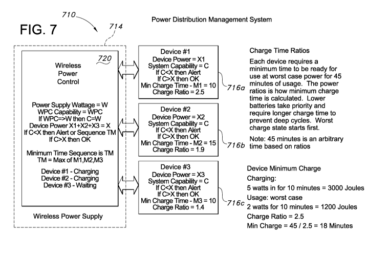
Fig. 7 shows yet another modification of the system in which power
distribution
from the wireless power supply 714 is managed by the wireless power control
720 at least
partially in response to power ratios from each secondary device 716a-c. This
embodiment
enables, for example, a single laptop charger to charge many laptops by
understanding the charge
status and by rotating the charge based on the charge ratio versus discharge.
For example, if
three laptops have a 2.5 charge ratio, each can be charged for 15 minutes and
get a 45 minute
use. This approach would enable a 15-minute cycle for all three units
consuming less overall
power and allowing a lower cost solution than device specific chargers.
18
CA 02748369 2011-06-27
WO 2010/080736 PCT/US2010/020061
The power ratio is how minimum charge time is calculated. Lower batteries take
priority and require longer charge time to prevent deep cycles. The worst-
charge state battery
starts charging first. The particular charge ratios and power times discussed
in this embodiment
are illustrative only. Existing secondary devices 716 are capable of
monitoring their respective
charge cycles.
Fig. 8 shows an example of the analog output used to select the wattage of the
power supply to implement the analog control method. The control wire 419
shown in Figure 4
carries the analog signal selected by the resistor configuration shown in the
table in Fig. 8. A
voltage is scaled, and the table is used to indicate the wattage capacity of
the power supply based
on the analog selection voltage on line 419 to wireless power supply 424. The
preferred method
is a digital communications signal for better resolution of limits and
capacity information.
Fig. 9 shows the data sequence between the wireless power supply 214 and the
device 216. Within the wireless power supply, the system powers up 901 and
reads the wattage
requested by the secondary devices. If a device is present 902, the device
identification is read
903. If a device is not present 902, then the system continues to monitor the
charger 904. If a
device identifier has been detected 903, then the device identification is
sent 904 to the
secondary device. If the device identification is not detected, the system
goes into standby mode
906 until the device wattage is greater than or equal to the load; and the
system indicates that the
load is incompatible.
Within the secondary device, if the device is compatible 907, then the
secondary
device is powered and/or charged 908. If the device is not compatible, a
decision 909 is made
regarding whether the device can charge at a lower rate. If the device cannot
charge at a lower
19
CA 02748369 2011-06-27
WO 2010/080736 PCT/US2010/020061
rate, then the device and/or the WPS indicate incompatibility 910. If the
device is capable of
charging at a lower rate, the device is powered 908 at that lower rate.
Fig. 10 shows a basic feedback mechanism including touch and/or sound. This
embodiment may be desirable when the user is driving and/or when the device is
set down to
charge. This method allows less interaction with the user and a positive
feedback for proper and
improper capacities.
As illustrated in Fig. 10, the current embodiment of the haptic feedback error
is
three vibrations with delays between each of the three vibrations. A haptic
feedback indicating
an acceptable condition is a single vibration. Of course, other numbers and/or
patterns of
vibrations could be used. These patterns would be different than ring, SMS, or
email indicators.
The present vibration motor used in a portable phone could easily be utilized
for such a feedback
device that could indicate compatibility or incompatibility without having to
see indicators. This
is especially favourable in automotive or driving environments.
As also illustrated in Fig. 10, feedback can be provided by way of sound such
as
beeps and/or tones with a specific intensity (loudness), frequency (pitch),
interval (pattern), and
timbre (sonority). The frequency, volume, pattern, and/or timber can change as
the secondary
gets closer to the primary. An exemplary error signal might be alternating
between low and high
pitch. As with the haptic feedback, indication of an acceptable match might be
provided with a
single beep, while indication of a incompatibility might be indicated by
multiple beeps such as
three beeps. If LEDs or other visual indicators are provided on the secondary
devices and/or the
WPS, one possible indication of compatibility is illuminating a visual
indicator continuously,
while an indication of incompatibility would be signed by cycling or flashing
the visual
indicator. Other indications might include display of one or more colors.
CA 02748369 2011-06-27
WO 2010/080736 PCT/US2010/020061
Fig. 11 shows a placement sequence table that provides exemplary outcomes and
events that can allow a complete charge for many situations while maintaining
system simplicity.
Fig. 11 is exemplary with all of the devices, wattages, sequencing, and other
variables being
readily variable as will be recognized by those skilled in the art.
Fig. 12 shows a four-unit charger using the present method. The wireless power
supply 1214 includes a plurality of primary coils LP1-LP4. Each coil includes
a switch
controlled by the WPS control 1220. The switches are controlled by the drive
control to
selectively charge the devices.
Fig. 13 shows a WPS 1314 in which additional capacity is provided without
needing full power supply coverage for proper distribution. Specifically, WPS
1314 includes
two drive controls 1320a and 1320b, each of which controls two primary coils.
Typically each
unit or coil would require the maximum power supply support per device. An
example of this
would be 4 to 5 watt devices or 20 watts. The example in Fig. 13 may provide
10 watts versus
Fig. 12 providing 5 watts. These are design configurable for best performance.
As one exemplary use, the WPS's 1214 and 1314 of Figs. 12 and 13 are
appropriate for conference room tables, airplane distribution systems,
automotive solutions, and
other applications with potentially limited power availability.
Fig. 14 shows a system 1410 and a related method of using the secondary device
power management unit (PMU) (not shown) in the secondary device 1416 to better
control,
regulate, and anticipate power fluctuations. These changes are communicated as
or before they
happen.
The system 1410 includes a power supply 1412, a wireless power supply 1414,
and a wireless power device 1416. All of these components are as previously
described.
21
CA 02748369 2011-06-27
WO 2010/080736 PCT/US2010/020061
Additionally, the PMU of the device 1416 communicates with the wireless power
control 1420
and the device control 1424.
Typical wireless power systems are reactive to the changes in load, and the
illustrated approach allows the systems to work together. Secondary commands
enable changes
based on expected variations. The wireless power supply 1414 uses the device
power
management unit (PMU) to track and respond to system needs by adjusting the
PID in
anticipation of the expected power required. This minimizes the time and
control issues noted
above associated with reacting to the new requirement.
One exemplary load requirement is illustrated in Fig. 14 in which the power is
stepped up from a basic power level to additionally sequentially power a
backlight and a hard
drive. Because the secondary device can anticipate such needs within the
device, the secondary
device control 1424 can let the wireless power control 1424 "know ahead of
time" when power
demands will change.
The wireless power control 1424 may communicate directly with the secondary
device's power management unit (PMU). That information may be injected into
the PID loop.
This approach enables the power supply to be built at a smaller capacity.
As described and illustrated, the current embodiments of the invention include
one or more of the following:
= A wireless power device with power reconciliation based on the capacity
of the primary
= A wireless power system that indicates power availability, warnings, and
charge sequence
22
CA 02748369 2011-06-27
WO 2010/080736 PCT/US2010/020061
= A wireless power distribution system that allocates power based on
available power, distribution, and device needs
= A device that can indicate power compatibility with a wireless power
supply
= A system having haptic, sound, and/or visual feedback for indicating
charging, sequencing (of secondary devices), or inability to charge a
secondary device
= A wireless power system that transmits wirelessly available capacity and
reads secondary device power needs, and reconciles power distribution,
sequencing, and availability
= A wireless power system capable of powering multiple secondary devices
on a single power supply using priority timing and charge ratios to manage
power sequencing
= A wireless power supply that can communicate basic commands from the
primary circuit to the secondary device for indicating power compatibility
to the user
= A wireless power supply that can sending simple commands for
configuring the secondary device for features such as mute, radio off,
vibrate, or fee required
= A wireless power supply that can communicate characteristics for
configuring the wireless power supply such as impedance and cord
resistance, and operating parameters such as voltage, current, and
tolerances
23
CA 02748369 2011-06-27
WO 2010/080736 PCT/US2010/020061
= A frequency-based wireless power supply using the rail voltage to control
power and send frequency modulated information from the primary to the
secondary control
= A frequency based wireless power supply that uses frequency modulation
to communicate to the secondary control
= A wireless power system that uses secondary device power management
information to control through a wireless link the response and
adjustments to changing load requirements
= A wireless power system that is connected to the secondary power
management system by way of a wireless link that is sent the PID error
information based on expected requirements and not measured error
anticipating changes as they happen by the power management unit
= A wireless power system having a PID control linked to the power
management system with preset error adjustments based on the devices
being used and the power required
= A wireless power supply using pre-calculated error percentages as a PID
control variable as power management systems are turned on and off
= A wireless power system including a basic indicator or logo on a charge
surface that has additional information that can be communicated to the
user for enhanced communications and understanding of the capabilities
of that system
24
CA 02748369 2011-06-27
WO 2010/080736 PCT/US2010/020061
The above descriptions are those of current embodiments of the invention.
Various alterations and changes can be made without departing from the spirit
and broader
aspects of the invention.