Note: Descriptions are shown in the official language in which they were submitted.
CA 02748597 2011-06-29
WO 2010/080694 PCT/US2010/000027
LIGHT EMITTING AND LASING SEMICONDUCTOR DEVICES
AND METHODS
FIELD OF THE INVENTION
This invention relates to methods and devices for producing light emission
and laser emission in response to electrical signals. An aspect of the
invention
also relates to methods for producing light emission and laser emission from
semiconductor transistor devices with improved efficiency. Another aspect of
the
invention relates to methods and devices for producing light emission and
laser
emission from two terminal semiconductor devices.
BACKGROUND OF THE INVENTION
A part of the background hereof lies in the development of wide bandgap
semiconductors to achieve high minority carrier injection efficiency in a
device
known as a heterojunction bipolar transistor (HBT). These transistor devices
are
capable of operation at extremely high speeds. For example, InP HBTs have, in
recent years, been demonstrated to exhibit operation at speeds above 500 GHz.
Another part of the background hereof lies in the development of
heterojunction bipolar transistors which operate as light-emitting transistors
and
transistor lasers. Reference can be made for example, to U.S. Patent Numbers
7,091,082, 7,286,583, 7,354,780, and 7,535,034; U.S. Patent Application
Publication Numbers US2005/0040432, US2005/0054172, US2008/0240173,
and US200910134939; and to PCT International Patent Publication Numbers
WO/2005/020287 and WO/2006/093883. Reference can also be made to the
following publications: Light-Emitting Transistor: Light Emission From
InGaP/GaAs Heterojunction Bipolar Transistors, M. Feng, N. Holonyak, Jr., and
W. Hafez, Appl. Phys. Left. 84, 151 (2004); Quantum-Well-Base Heterojunction
Bipolar Light-Emitting Transistor, M. Feng, N. Holonyak, Jr., and R. Chan,
Appl.
CA 02748597 2011-06-29
WO 2010/080694 PCT/US2010/000027
2
Phys. Lett. 84, 1952 (2004); Type-II GaAsSb/InP Heterojunction Bipolar Light-
Emitting Transistor, M. Feng, N. Holonyak, Jr., B. Chu-Kung, G. Walter, and R.
Chan, Appl. Phys. Lett. 84, 4792 (2004); Laser Operation Of A Heterojunction
Bipolar Light-Emitting Transistor, G. Walter, N. Holonyak, Jr., M. Feng, and
R.
Chan, Appl. Phys. Lett. 85, 4768 (2004); Microwave Operation And Modulation
Of A Transistor Laser, R. Chan, M. Feng, N. Holonyak, Jr., and G. Walter,
Appl.
Phys. Lett. 86, 131114 (2005); Room Temperature Continuous Wave Operation
Of A Heterojunction Bipolar Transistor Laser, M. Feng, N. Holonyak, Jr., G.
Walter, and R. Chan, Appl. Phys. Left. 87, 131103 (2005); Visible Spectrum
Light-Emitting Transistors, F. Dixon, R. Chan, G. Walter, N. Holonyak, Jr., M.
Feng, X. B. Zhang, J. H. Ryou, and R. D. Dupuis, Appl. Phys. Lett. 88, 012108
(2006); The Transistor Laser, N. Holonyak and M Feng, Spectrum, IEEE
Volume 43, Issue 2, Feb. 2006; Signal Mixing In A Multiple Input Transistor
Laser Near Threshold, M. Feng, N. Holonyak, Jr., R. Chan, A. James, and G.
Walter, Appl. Phys. Left. 88, 063509 (2006); and Collector Current Map Of Gain
And Stimulated Recombination On The Base Quantum Well Transitions Of A
Transistor Laser, R. Chan, N. Holonyak, Jr., A. James, and G. Walter, Appl.
Phys. Left. 88, 14508 (2006); Collector Breakdown In The Heterojunction
Bipolar
Transistor Laser, G. Walter, A. James, N. Holonyak, Jr., M. Feng, and R. Chan,
Appl. Phys. Left. 88, 232105 (2006); High-Speed (/spI ges/1 GHz) Electrical
And
Optical Adding, Mixing, And Processing Of Square-Wave Signals With A
Transistor Laser, M. Feng, N. Holonyak, Jr., R. Chan, A. James, and G. Walter,
Photonics Technology Letters, IEEE Volume: 18 Issue: 11 (2006); Graded-Base
InGaN/GaN Heterojunction Bipolar Light-Emitting Transistors, B. F. Chu-Kung et
al., Appl. Phys. Left. 89, 082108 (2006); Carrier Lifetime And Modulation
Bandwidth Of A Quantum Well AIGaAs/InGaP/GaAs/InGaAs Transistor Laser,
M. Feng, N. Holonyak, Jr., A. James, K. Cimino, G. Walter, and R. Chan, Appl.
Phys. Left. 89, 113504 (2006); Chirp In A Transistor Laser, Franz-Keldysh
Reduction of The Linewidth Enhancement, G. Walter, A. James, N. Holonyak,
Jr., and M. Feng, Appl. Phys. Lett. 90, 091109 (2007); Photon-Assisted
Breakdown, Negative Resistance, And Switching In A Quantum-Well Transistor
CA 02748597 2011-06-29
WO 2010/080694 PCT/US2010/000027
3
Laser, A. James, G. Walter, M. Feng, and N. Holonyak, Jr., Appl. Phys. Lett.
90,
152109 (2007); Franz-Keldysh Photon-Assisted Voltage-Operated Switching of
a Transistor Laser, A. James, N. Holonyak, M. Feng, and G. Walter, Photonics
Technology Letters, IEEE Volume: 19 Issue: 9 (2007); Experimental
Determination Of The Effective Minority Carrier Lifetime In The Operation Of A
Quantum-Well n-p-n Heterojunction Bipolar Light-Emitting Transistor Of Varying
Base Quantum-Well Design And Doping; H.W. Then, M. Feng, N. Holonyak, Jr.,
and C. H. Wu, Appl. Phys. Left. 91, 033505 (2007); Charge Control Analysis Of
Transistor Laser Operation, M. Feng, N. Holonyak, Jr., H. W. Then, and G.
Walter, Appl. Phys. Left. 91, 053501 (2007); Optical Bandwidth Enhancement By
Operation And Modulation Of The First Excited State Of A Transistor Laser, H.
W. Then, M. Feng, and N. Holonyak, Jr., Appl. Phys. Left. 91, 183505 (2007);
Modulation Of High Current Gain (0>49) Light-Emitting InGaN/GaN
Heterojunction Bipolar Transistors, B. F. Chu-Kung, C. H. Wu, G. Walter, M.
Feng, N. Holonyak, Jr., T. Chung, J.-H. Ryou, and R. D. Dupuis, Appl. Phys.
Left.
91, 232114 (2007); Collector Characteristics And The Differential Optical Gain
Of A Quantum-Well Transistor Laser, H. W. Then, G. Walter, M. Feng, and N.
Holonyak, Jr., Appl. Phys. Left. 91, 243508 (2007); Transistor Laser With
Emission Wavelength at 1544 nm, F. Dixon, M. Feng, N. Holonyak, Jr., Yong
Huang, X. B. Zhang, J. H. Ryou, and R. D. Dupuis, Appl. Phys. Left. 93, 021111
(2008); and Optical Bandwidth Enhancement Of Heterojunction Bipolar
Transistor Laser Operation With An Auxiliary Base Signal, H.W. Then, G.
Walter,
M. Feng, and N. Holonyak, Jr. Appl. Phys. Left. 93, 163504 (2008).
The basis of a fast transistor is in its ability to enhance electron-hole pair
recombination through the large build in majority carriers in the base, fast
transport of minority carriers through the base, and the collection mechanism
(electrical collector) that collects unrecombined minority carriers out of the
base
region; all of which supports the fast charging and discharging of charge
storage
capacitance in the base region.
Optical operation of a heterojunction bipolar light emitting transistor
(HBLET), as described in the above-referenced Patents and publications,
CA 02748597 2011-06-29
WO 2010/080694 PCT/US2010/000027
4
depends on the radiative recombination component in the base region which
typically occurs dominantly in an embedded quantum size region in the base,
for
example an undoped quantum well (QW). Together, the sum of the non-radiative
recombination current component (Inon-rad) which dominantly occurs in the
highly
doped region of the base, and radiative recombination component (Irad) in the
base, is equal to the supplied base current (lb= Inon-rad + Irad)=
The addition of a QW in a base region allows the incorporation of an
efficient radiative recombination center. From a 1-dimensional point of view,
carriers are captured in the QW and recombined radiatively, or swept out of
the
base into the electrical collector. However, in reality, captured carriers do
not
recombine immediately, resulting in potential charge build up in the quantum
well. Carriers that are accumulating in the quantum well region would
redistribute
through efficient lateral diffusion, spreading carriers and recombination
events
sideways and away from the optical cavity of the device. Captured carriers
could
also simultaneously re-thermalize back into the base region as they travel
laterally.
It is among the objects of an aspect hereof to overcome limitations of prior
art light-emitting transistors (LETs) and transistor lasers (TLs), for example
the
type of limitation described just above.
Another part of the Background hereof relates to the need for
improvement in two terminal light emitters for certain applications.
Due to the increasing demand for transfer and storage for high definition
digital video data, high speed communication links are starting to traverse
the
consumer electronic market at link speeds once demanded almost exclusively
only in the commercial market, via standards such as HDMI 1.3 and 1.4, USB
3.0, Displayport 2.0 and PCI2Ø However, the increasing higher data speed,
now
approaching -6.8 Gbps/channel for the new HDMI 1.4 standard, adds design,
technical and manufacturing complexity on the traditional transmission media
via
copper wire. The results are consumer products that are increasingly bulkier,
unaesthetic and inflexible.
CA 02748597 2011-06-29
WO 2010/080694 PCT/US2010/000027
Fiber based communication links have long since started to replace
copper media links, but mainly at non-consumer market distances of larger than
30 meters. At distances of less than 5 meters, where the bulk of the consumer
market is, VCSEL (vertical cavity surface emitting lasers) based optical
solutions
are unable to compete based on price and even power consumption.
The study of the transistor base transport mechanism led to the
emergence of a new class of high speed (>1 GHz) tilted charge spontaneous
light emitters as the quantum well light emitting transistor (QW-LET) and the
transistor laser (TL) that are promisingly much cheaper to manufacture or
operate than traditional diode laser devices (see e.g. the above-listed Patent
documents and publications). Unfortunately, widely available low cost high
speed driver ICs and biasing circuitry, and opto-manufacturing facilities are
built
upon two terminal devices such as LEDs and laser diodes. Therefore, the
transition from a two terminal devices to three terminal devices requires
supporting industry (e.g. IC designers, and manufacturing facilities) to also
transition, which then delays and increases the cost of implementing the QW-
LET and TL.
It is among the objectives of the present invention to devise a two terminal
semiconductor light emitter or laser that has advantages over existing
semiconductor light emitter and lasers, including simplicity of design, ease
of
fabrication, and the capability of efficient high speed light generation, and
which
also has certain attributes of three terminal light emitting transistors or
transistor
lasers, but which is compatible with applications that favor or require two
terminal
operation.
SUMMARY OF THE INVENTION
As above-indicated, captured carriers do not recombine immediately,
resulting in potential charge build-up in the quantum well (of, for example,
an LET
or TL), and accumulating carriers redistribute through lateral diffusion,
thereby
spreading carriers and recombination events sideways and away from the
CA 02748597 2011-06-29
WO 2010/080694 PCT/US2010/000027
6
device's optical cavity. Captured carriers could also simultaneously re-
thermalize
back into the base region as they travel laterally.
Applicant believes that one of the main factors leading to the saturation
behavior and reduced quantum efficiency in the described devices is the
rethermalization of carriers back towards the emitter side (back diffusion).
Therefore, in accordance with one aspect hereof, an asymmetric base design is
employed to minimize the non-radiative recombination component due to the
back diffusion of carriers.
In accordance with a form of the first aspect the invention, a method is set
forth for improving operation of a light emitting transistor, including the
following
steps: providing a light emitting transistor that includes emitter, base, and
collector semiconductor regions, and a quantum size region within the base
region, the base region comprising a first base sub-region on the emitter side
of
said quantum size region, and a second base sub-region on the collector side
of
said quantum size region; and providing said first and second base sub-regions
with asymmetrical band structures. In an embodiment of this form of the
invention, the step of providing the first and second base sub-regions with
asymmetrical band structures comprises providing the first base sub-region
with
a higher bandgap semiconductor material than the semiconductor material of the
second base sub-region. In one version of this embodiment, the step of
providing the first base sub-region with a higher bandgap semiconductor
material
than the semiconductor material of the second base sub-region includes
providing the first base sub-region with a graded bandgap semiconductor
material. The graded bandgap semiconductor material is graded to have a
gradually increasing bandgap in the direction of said emitter. In another
version
of this embodiment, the step of providing the first base sub-region with a
higher
bandgap semiconductor material than the semiconductor material of the second
base sub-region includes providing the first base sub-region with a stepped
bandgap semiconductor material. In a further versionof this embodiment, the
step of providing the first base sub-region with a higher bandgap
semiconductor
material than the semiconductor material of the second base sub-region
includes
CA 02748597 2011-06-29
WO 2010/080694 PCT/US2010/000027
7
providing the first base sub-region with a graded and stepped bandgap
semiconductor material.
In accordance with another form of the first aspect of invention, a
semiconductor light emitting device is provided, comprising: a heterojunction
bipolar light-emitting transistor having a base region between emitter and
collector regions; emitter, base, and collector electrodes for coupling
electrical
signals with the emitter, base, and collector regions, respectively; and a
quantum
size region in the base region; the base region including a first base sub-
region
on the emitter side of the quantum size region, and a second base sub-region
on
the collector side of the quantum size region; and the first and second base
sub-
regions having asymmetrical band structures. A resonant optical cavity can
enclose at least a portion of the base region, whereby the device can comprise
a
transistor laser. In an embodiment of this form of the invention, the quantum
size
region within the base region comprises at least one quantum well within the
base region. In another embodiment of this form of the invention, the quantum
size region within the base region comprises at least one layer of quantum
dots
within the base region.
Next, a second aspect of the invention is treated.
A transistor is a device having of two semiconductor junctions; the Base-
Emitter (BE) Junction and the Collector-Base (CB) Junction. To operate as a
transistor, the BE junction is required to be at low impedance (forward bias
(see
Fig 17a), typically VBE > 1.2 V), while the Collector-Base junction is
required to be
at high impedance ((See Fig. 17b), typically 0.8 > VCB > -5 V). Under common
collector configuration, a collector is generally grounded (0 V) and VE and VB
are
selected so that transistor bias is maintained (VBE > 1.2 V, and 0.8 > VCB > -
5 V),
as shown in Fig 18.
Applicant has noted, however, that there exists a special condition where
VB = VC = 0 (hence VCB = 0 V, see Fig. 19a), and therefore also fulfilling the
transistor requirement. that 0.8 > VCB > -5 V for high impedance operation in
a
typical high speed HBT (e g. InGaP/GaAs HBT). This condition also implies that
the base and collector terminals can be electrically connected (on the device
CA 02748597 2011-06-29
WO 2010/080694 PCT/US2010/000027
8
through fabrication or externally) while still maintaining transistor
operation (see
Fig 19b).
A transistor laser is a three terminal and two port electrical device, where
a first electrical input has low impedance, and current (known as collector
current) is drawn from the high impedance second electrical output. The device
also has an optical output port. [Reference can be made to the Patent
documents and publication documents referenced in the Background portion
hereof.] In a conventional transistor, this transfer of electrical impedance
(or
resistance) from low-to-high, was the genesis of its name; that is, the
"transfer
resistor" device or "transistor". A measurable collector current is critical
to the
operation of a transistor. However, a main factor that supports fast operation
of
the transistor laser (in an NPN transistor laser, for example) is the
mechanism
that helps eliminate injected electrons that did not recombine in the highly
doped
base region of the transistor - and this is achieved by the use of a high
impedance collector design.
However, having two electrical ports can complicate fabrication, affecting
both yield and cost. Also, for certain applications it is necessary or
desirable to
have only one electrical input port and an optical output.
It is possible, in accordance with a second aspect hereof, that the intrinsic
fast operation of the light emitting transistor or transistor laser can still
be
maintained in a two terminal device (i.e., single electrical input port
device) by
replacing the collector junction with a drain. The drain serves the same
purpose
of allowing excess electrons to exit the N-P (Emitter-Base) junction of the
device.
However, it eliminates the functionality of this excess current (since it is
no longer
excess current to be collected but rather eliminated) by draining the
electrons
towards non-radiative recombination at the common contact. The drain is
required to operate at high impedance mode, which can be achieved by having a
common bias with the P-terminal of the base.
In accordance with a form of the second aspect of the invention, a method
is set forth for producing light emission from a semiconductor structure,
including
the following steps: providing a semiconductor structure that includes a first
CA 02748597 2011-06-29
WO 2010/080694 PCT/US2010/000027
9
semiconductor junction between an emitter region of a first conductivity type
and
a base region of a second conductivity type opposite to that of said first
conductivity type, and a second semiconductor junction between said base
region and a drain region; providing, within the base region, a region
exhibiting
quantum size effects; providing an emitter electrode coupled with the emitter
region; providing a base/drain electrode coupled with the base region and the
drain region; and applying signals with respect to the emitter and base/drain
electrodes to obtain light emission from said semiconductor structure.
In a preferred embodiment of this form of the second aspect of the
invention, the step of providing the second semiconductor junction between the
base region and the drain region includes providing the drain region as a
drain
layer adjacent the base region and a sub-drain layer adjacent the drain layer,
and
wherein said step of providing a base/drain electrode coupled with the base
region and the drain region comprises providing a base/drain electrode coupled
with the base region and the sub-drain layer. In this embodiment, the step of
providing a semiconductor structure comprises providing planar semiconductor
layers, and the step of providing a base/drain electrode comprises providing a
conductive base/drain contact that contacts the periphery of the base region,
and
contacts the sub-drain layer. Also in this embodiment, the step of providing a
first semiconductor junction between the emitter region of the first
conductivity
type and the base region of a second conductivity type comprises providing the
first semiconductor junction as a heterojunction. The second semiconductor
junction can be provided as a homojunction or a heterojunction.
In accordance with another form of the second aspect of the invention, a
semiconductor device is set forth for producing light emission, comprising: a
semiconductor structure that includes a first semiconductor junction between
an
emitter region of a first conductivity type and a base region of a second
conductivity type opposite to that of said first conductivity type, and a
second
semiconductor junction between the base region and a drain region; a quantum
size region within the base region; an emitter electrode coupled with the
emitter
region; and a base/drain electrode coupled with the base region and the drain
CA 02748597 2011-06-29
WO 2010/080694 PCT/US2010/000027
region; whereby signals applied with respect to said emitter and base/drain
electrodes produce light emission from the base of the semiconductor device.
The two-terminal devices of the second aspect of the present invention
retain the fast transistor base transport mechanism of LETs and TLs while
allowing the device to be compatible with existing diode circuitries and
manufacturing facilities As a two terminal device it will also tend to be
cheaper to
manufacture and package than the three terminal devices. For example, it
requires fewer lithography steps, fewer bonding pads, and less fabrication
time,
and will provide a higher yield.
Further features and advantages of the invention will become more readily
apparent from the following detailed description when taken in conjunction
with
the accompanying drawings.
BRIEF DESCRIPTION OF THE DRAWINGS
Figure 1 is a graph showing measured photon output from a quantum
well-heterojunction bipolar light emitting transistor as a function of base
current.
Figure 2 is an energy band diagram for a typical quantum well in a base
region, which is useful in understanding the thermalization current phonomena.
Figure 3 is an energy band diagram for a Type 1 arrangement of the first
aspect hereof with the material of the first base sub-region on the emitter
side of
the quantum well having a larger bandgap than the material of the second base
sub-region on the collector side of the quantum well.
Figure 4 is an energy band diagram for a Type 2 arrangement of the first
aspect hereof, with a graded wide bandgap structure of the first base sub-
region.
Figure 5 is an energy band diagram for a Type 3 arrangement of the first
aspect hereof, with the first base sub-region having a stepped bandgap.
Figure 6 is an energy band diagram for a Type 4 arrangement of the first
aspect hereof, with the first base sub-region having a graded and then stepped
bandgap.
Figure 7 is an energy band diagram of a device in accordance with an
embodiment of the first aspect hereof which in this example is an npn light-
CA 02748597 2011-06-29
WO 2010/080694 PCT/US2010/000027
11
emitting transistor or transistor laser which includes a base region having a
quantum well and an asymmetrical band structure on opposite sides of the
quantum well.
Figure 8 is a cross-sectional view of a conventional QW-heterojunction
bipolar light emitting transistor (QW-HBLET) with a deep QW design and
homogenous doped base region. (Drawings are not to scale.)
Figure 9 is a cross-sectional view of a QW-HBLET structure in accordance
with an embodiment of the first aspect hereof, having an asymmetric base
design
in order to eliminate or reduce rethermalization of carriers towards the
emitter.
Figure 10 is a cross-sectional view of a QW-HBLET structure in
accordance with a further embodiment of the first aspect hereof, having an
asymmetric base design to reduce rethermalization of carriers towards the
emitter side and use of one or more shallow quantum well(s) [QW(s)] in order
to
limit the lateral diffusion of captured carriers.
Figure 11 is a diagram of the basic layer structure of a QW-HBLET with
asymmetric base in accordance with an embodiment of the first aspect of the
invention.
Figure 12 shows a Table with a more detailed example of the layer
structure of a QW-HBLET in accordance with an embodiment of the first aspect
of the invention, and which employs a first base sub-region graded to have a
gradually increasing bandgap in the direction of the emitter.
Figure 13 is a Table showing an example of the layer structure of a QW-
HBLET having asymmetrical base design, in accordance with the principles of
the first aspect hereof, and provided with a resonant cavity (RC) and called a
QW-RCLET.
Figure 14 is a Table showing an example of the layer structure of a
quantum well vertical cavity transistor laser (QW-VCTL), having an
asymmetrical
base design in accordance with the principles of the first aspect hereof.
Figure 15 is a Table showing an example of the layer structure of a
quantum well-heterojunction bipolar transistor laser (QW-HBTL) with an edge
emitting design (that can employ reflective edge facets) and having an
CA 02748597 2011-06-29
WO 2010/080694 PCT/US2010/000027
12
asymmetrical base design in accordance with the principles of the first aspect
hereof.
Figure 16 is a partially broken away diagram of the basic layer structure of
a QW-HBLET as in Figure 11, but modified to employ a tunnel junction
collector.
Figure 17a shows a simplified transistor I vs. VBE Plot.
Figure 17b shows a simplified transistor I vs. VCB Plot.
Figure 18 shows an example of a transistor in common collector
configuration.
Figure 19a shows a transistor in common collector configuration, in a
special biasing condition that still maintains transistor operation.
Figure 19b shows a transistor configuration with base and collector
terminals electrically connected, while maintaining transistor operation.
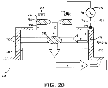
Figure 20 shows a cross-sectional view of a two junction light emitting
diode in accordance with an embodiment of the second aspect of the invention,
and which can be used in practicing an embodiment of the method of the
invention.
Figure 21 shows, on the left in (a), an equivalent DC circuit of a two
junction diode, and, on the right in (b), the IE vs. V characteristic. The
second
junction functions to reduce the overall resistance of the circuit by allowing
the
base layer to mainly conduct holes, and electrons are conducted by the N-type
drain.
Figure 22 shows, on the left in (a), an equivalent circuit of a single
junction
diode as in the prior art, and, on the right in (b), the IE VS. V
characteristic. The
base layer is responsible for both the flow of holes and minority electrons.
Figure 23 shows an oscillograph display of optical output (optical detector
voltage) as a function of time for an embodiment of the second aspect of
hereof.
The display shows a 5 Gbps eye at 15 degrees C at an emitter current of 70 mA.
The time scale is 50 picoseconds per division.
Figure 24 shows another oscillograph display of optical output as a
function of time for an embodiment of the second aspect of hereof. The display
CA 02748597 2011-06-29
WO 2010/080694 PCT/US2010/000027
13
shows a 10.3125 Gbps eye at an emitter current of 100 mA. The time scale is 20
picoseconds per division.
Figure 25 shows a cross-sectional view of another embodiment of the
second aspect of hereof.
DETAILED DESCRIPTION
Applicant has observed that the radiative recombination component does
not increase linearly with base current. Figure 1 shows measured photon output
from a QW-HBLET exhibiting saturation behavior (departure from linear curve)
at
higher base current indicating an increase in non-radiative recombination
component. In addition, Applicant has also observed that the radiative
recombination component is also a strong function of temperature. These
observations further suggest that non-radiative recombination activity, and
therefore bulk base recombination, also increases as a function of both
current
density and temperature.
Referring to Figure 2, which shows an energy band diagram for a typical
quantum well in a base region, the thermalization current (Ithemad) depends
mainly
on two variables, phonon energy (proportionate to temperature, T) and the
barrier height (V) in which the carriers are confined, as seen from the
following
relationships:
qV1
(X El
GVz:
e des.
'.7 a man
e k7
{.tharmad2
where q is the coulomb charge 1.6 x 10"19 C, and k is the Boltzman constant.
Captured carriers in the quantum well thermalize out of the quantum well
through
the assistance of phonons. For a symmetrical quantum well (AV = V1-V2= 0), the
probability of the carriers thermalizing to either side of QW is equal, "hor'
is =
, Wade
The equations above also show that a deep QW (large V1,V2) reduces the
CA 02748597 2011-06-29
WO 2010/080694 PCT/US2010/000027
14
thermal current as a whole. However, a deeper QW increases the QW ability to
store charge which will significantly decrease the high speed capability of
the
device. Due to better confinement of captured carriers, a deep QW is also more
efficient regarding lateral diffusion of captured carriers. On the other
extreme, the
use of shallow well increases the rethermalization rate of captured carriers
that
competes with the recombination rate of the QW, which could lead to a high
gain
device. In accordance with a feature hereof, one or more relatively shallow
QWs
can be employed, thereby achieving advantages of speed and high gain, but
without the concomitant re-thermalization problems that might normally dictate
against the use of shallow well(s) - since the relatively higher bandgap first
base
sub-region will tend to reduce re-thermalized carriers movement toward the
emitter region. These carriers will tend to flow back into the QW(s). In an
embodiment hereof, the shallow well(s) used in conjunction with the
asymmetrical base feature are limited to have a single energy state; that is,
the
ground state.
Figure 3 shows a Type 1 arrangement with the material of the first base
sub-region on the emitter side having a larger bandgap than the material of
the
second base sub-region on the collector side. This arrangement provides the
largest possible Ithermall/Ithermal2 ratio. However, most large bandgap
materials have relatively lower mobility that reduces the transit time of
carriers.
Figure 4 shows a Type 2 arrangement. A graded wide bandgap structure
for the first base sub-region allows a built-in field that assists in the
transit of
carriers, therefore reducing the impact of lower intrinsic mobility of higher
bandgap material. The graded field also assists any rethermalized carriers in
the
first base sub-region to flow back into the quantum well. The effective
barrier
height (Vi) is lower than that in the Type 1 structure due to the graded
effect.
Figure 5 shows a Type 3 arrangement with the first base sub-region
having a stepped bandgap. In this example, the wide bandgap material is grown
after an undoped or low doped buffer layer is grown. A buffer layer may be
necessary for material growth purposes.
CA 02748597 2011-06-29
WO 2010/080694 PCT/US2010/000027
Figure 6 shows a Type 4 arrangement with the first base sub-region
having a graded and then stepped bandgap. The wide bandgap material is
grown after an undoped or low doped graded buffer layer is grown. A graded
buffer helps thermalized carriers to be swept back into the quantum well,
minimizing the recombination event in the buffer layer. Low doped or undoped
layers minimizes the non-radiative recombination capability of that layer.
Referring to Figure 7, there is shown an energy band diagram of a device
in accordance with an embodiment of a first aspect hereof hereof which in this
example is an npn light-emitting transistor or transistor laser which includes
a
base region having a quantum well and an asymmetrical band structure on
opposite sides of the quantum well. Under ideal conditions, thermalization of
carriers should only be towards the collector where it can be collected. The
widest bandgap region of the base is chosen in such that the valence band
discontinuity (OVv) is still larger than 0 V in order to prevent the diffusion
of holes
into the emitter. The graded bandgap of the base assists, through a built-in
electric field, in drifting electrons toward the electrical and optical (QW)
collectors.
It also assists in drifting built-in holes towards the collector.
Referring to Figure 8, there is shown a conventional QW-heterojunction
bipolar light emitting transistor (QW-HBLET) with a deep QW design and
homogenous doped base region. Reference can be made, for example, to the
Patents and publications referenced in the Background portion hereof. In
Figure
8, the base region 840 is disposed between emitter region 850 and collector
region 830, the base region including quantum well 841. Below collector 830 is
a
sub-collector region 825 which has collector electrode 826 thereon. Above the
emitter is the emitter confining and contact region 860 and oxide-defined
aperture 855. The base region has base electrode 843 thereon, and the emitter
region has emitter electrode 853 thereon. Appropriate biasing and excitation
signals are applied to the electrodes as described, for example, in the
Patents
and publications listed in the Background portion hereof. The relatively deep
QW
assists captured carriers to spread laterally and recombine away from the
optical
cavity (shaded region 802 for this vertical cavity device). In addition to
that, as
CA 02748597 2011-06-29
WO 2010/080694 PCT/US2010/000027
16
the carriers spread laterally (see arrows), the carriers can also rethermalize
and
carriers that rethermalize towards the emitter (back diffusion) are mostly
lost to
non-radiative recombination.
Figure 9 shows a QW-HBLET structure in accordance with an
embodiment of the first aspect hereof, having an asymmetric base design in
order to eliminate or reduce rethermalization of carriers towards the emitter.
In
Figure 9, the emitter region 850, collector region 830, subcollector 825,
emitter
confining and contact region 860, oxide-defined aperture 855, emitter
electrode
853, base electrode 843, and collector electrode 826, are all similar to
elements
of like reference numerals in Figure 8. However, in Figure 9, the base 940 is
provided with a relatively wider bandgap base sub-region 948 on the emitter
side
as compared to a relatively narrow bandgap sub-region 947 on the collector
side.
The Figure 9 arrows (i.e., the absence thereof in the base upper sub-region)
represent the reduction in back diffusion. As described above, the higher
bandgap sub-region can preferably be achieved by providing the sub-region with
a graded bandgap semiconductor materials and/or stepped bandgap
semiconductor materials.
Figure 10 shows a QW-HBLET structure in accordance with a further
embodiment of the first aspect hereof, having an asymmetric base design to
reduce rethermalization of carriers towards the emitter side and use of one or
more shallow quantum well(s) [QW(s)] in order to limit the lateral diffusion
of
captured carriers. In Figure 10, like reference numerals represent similar
elements of the devices of Figures 8 and 9. In Figure 10, as in Figure 9, the
base region (1040, in Figure 10) has a relatively wider bandgap base sub-
region
(1048, in Figure 10) on the emitter side of the base as compared to a
relatively
narrower bandgap sub-region (1047, in Figure 10) on the collector side of the
base. In this case, however, as above noted, a shallower quantum well 1041 is
used in the base, in order to limit the lateral diffusion of captured carriers
(see
relatively shorter arrows in the lateral direction in Figure 10).
Figure 11 shows the basic layer structure of a QW-HBLET with
asymmetric base in accordance with an embodiment of the first aspect of the
CA 02748597 2011-06-29
WO 2010/080694 PCT/US2010/000027
17
invention. In this example, the device is npn, although it will be understood
that
the principles hereof also apply to pnp devices. The substrate 1105 (doped or
undoped) has deposited thereon an n-type lower confining layer 1110 with
oxidizable aperture layer, an n-type collector contact layer 1120 and an n-
type
collector layer 1130. The heavily doped p-type base region 1140 includes a
quantum well (QW) 1141, and sub-regions 1147 and 1148, with asymmetric
design of their bandgaps, as previously described. Also shown are the n-type
emitter 1150, n-type upper confining layer with oxidation aperture layer
(1160),
and emitter contact layer 1170.
The table of Figure 12 shows a more detailed example of the layer
structure of a QW-HBLET in accordance with an embodiment of the first aspect
of the invention, and which employs a first base sub-region graded to have a
gradually increasing bandgap in the direction of the emitter. Upward from the
GaAs substrate, the epitaxial layers of the crystal used for the QW-HBLET
include a 3000 A n-type doped GaAs buffer layer (Layer 1), a 500 A graded
Alo.3oGao.70As confining layer (Layer 2), a 213 A graded AI0.3oGao.7oAs to
Al0.90Ga0.1QAs oxide buffer layer (Layer 3), a 595 A n-type Alo.98Ga0.02As
oxidizable aperture layer (Layer 4), another 213 A of graded Al0.90Ga0.10As to
AIo.3oGa0,70As oxide buffer layer (Layer 5), followed by a 557 A n-type GaAs
contact layer (Layer 6 and 7), a 120 A InGaP etch stop layer (Layer 8), a 2871
A
undoped collector layer. These layers are followed by 1358 A of base layers
(Layer 19 to 18) which includes two undoped 112 A InGaAs quantum wells
(Layer 12 to 16), and a graded Alo.oo5Gao.995As to AI0.05Ga0.95As base layer
with
graded base doping (Layer 17).
Later, a heterostructure emitter including a 511 A n-type Ino.49Gao.51P layer
(Layer 19), a 213 A graded Al0330Ga0.70As to Alo.9oGao.loAs oxide buffer layer
(Layer 20), a 595 A n-type Al0.98Gao.02As oxidizable aperture layer (Layer
21),
another 213 A of graded Alo.90Ga0.10As to AI0.30Gao3oAs oxide buffer layer
(Layer
22), a 500 A graded AIo.3oGa0.70As confining layer (Layer 23). The structure
is
completed with a 2000 A GaAs top contact layer (Layer 24).
CA 02748597 2011-06-29
WO 2010/080694 PCT/US2010/000027
18
An example of the QW-HBLET fabrication process for an embodiment of
the first aspect hereof is performed by first patterning protective SiN4 on
the
crystal with a photolithography step and reactive ion etching with Freon 14
(CF4)
gas. The top n-type GaAs contact layer (Layer 24) and AlGaAs layers (Layer 20
to 23) are then exposed by wet etching (1:8:80 H202:H2SO4:H20) to form the
emitter mesa and reveal the n-type In0.a9Ga0.51P wide-gap emitter layer (Layer
19). The sample is oxidized at 425 C in a furnace supplied with N2+H2O,
resulting in lateral oxidation which forms oxide-defined apertures in the
emitter
mesa. The samples are annealed (in N2) at 425 C for 7 minutes to reactivate p-
dopants before the protective SiN4 is removed by plasma (CF4) etching. The
emitter layer (Layer 19), In0.49Ga0.51 P, is then removed using a wet etch
(HCI),
exposing the p-type AIGaAs base contact layer (Layer 18). A protective
photoresist (PR) layer, is then patterned to outline the base mesa. Layers 9
to
18 are then removed using a selective etch (10:1 C61-180-7:1-1202), and the
In0.49Ga0.51P etch-stop layer (Layer 8) is removed by a wet etch (HCI),
exposing
the heavily doped n-type GaAs sub-collector contact layer (Layer 7), and to
form
the base mesa. Later, a PR window is formed over the emitter mesa and the
collector material, followed by the deposition of AuGe/Ni/Au (750/150/10000 A)
to
form n-type metal contacts to the emitter contact layer (Layer 29), and sub-
collector contact layer (Layer 7). A metal lift-off process then follows.
Later,
another PR window is formed over the base mesa and after which Ti/Pt/Au
(250/80/1100 A) is deposited on layer 18 to form the P-type contact. After the
metal lift-off step, the sample is then annealed at 350 C to form ohmic
contacts.
Then a layer of polyimide is applied and cured at 270 C to reduce the surface
leakage current of the device. An additional layer of silicon nitride is
deposited
on top of the polyimide using the plasma-enhanced chemical vapor deposition
(PECVD) system. Via hole openings to create contacts to emitter, base, and
collector metals are defined using another photolithography step. Using Freon
14 (CF4) gas and PR as an etch mask, the dielectric via opening to the silicon
nitride layer is performed with a reactive ion etching (RIE) system. The PR is
then stripped with cleaning solvents. Oxygen (02) plasma is used to remove the
CA 02748597 2011-06-29
WO 2010/080694 PCT/US2010/000027
19
polyimide layer with the silicon nitride layer acting as an etch mask. After
the
contact via fabrication step, another photolighography step can be performed
to
deposit Ti/Au (150 A/ 2.5 pm) to form contacts from the device to the ground-
signal-ground (GSG) high frequency probing pads.
The table of Figure 13 shows an example of the layer structure of a QW-
HBLET having asymmetrical base design, in accordance with the principles of
the first aspect hereof, and provided with a resonant cavity (RC) and called a
QW-RCLET. Distributed Bragg reflector (DBR) mirrors are added to the HBLET
to form a resonant cavity to assist in light extraction. Top mirror reflection
is can
be varied from 1 % to 95% to form a resonant cavity light emitting transistor.
The
structure can also be reversed where the top DBR has more reflection than the
bottom DBR, which allows for light extraction through the substrate.
The table of Figure 14 shows an example of the layer structure of a
quantum well vertical cavity transistor laser (QW-VCTL), having an
asymmetrical
base design in accordance with the principles of the first aspect hereof. The
number of top DBR mirror pairs are increased to enable stimulated emission to
occur in a resonant vertical cavity transistor laser. Top mirror reflectivity
can be
varied from 90% to 99.5%. Likewise, the DBR mirror configuration can be
reversed for light extraction through the bottom.
The table of Figure 15 shows an example of the layer structure of a
quantum well-heterojunction bipolar transistor laser (QW-HBTL) with an edge
emitting design (that can employ reflective edge facets) and having an
asymmetrical base design in accordance with the principles of the first aspect
hereof. Thicknesses in layer 4 and 21 are increased to 3000 A in order to
allow
waveguiding effects.
Figure 16 shows a variation of the device of Figure 11 in which a tunnel
junction 1630 is utilized instead of the device's collector. Reference can be
made, for example, to Tunnel Junction Transistor Laser, M. Feng, N. Holonyak,
Jr., H.W. Then, C.H. Wu, and G. Walter, Appl. Phys. Left. 94, 04118 (2009),
with
regard to employing a tunnel junction as a collector in an HBTL. In Figure 16,
the
p+ layer 1631 of the tunnel junction 1630 is adjacent the base sub-region
1147,
CA 02748597 2011-06-29
WO 2010/080694 PCT/US2010/000027
and the n+ layer 1632 of the tunnel junction 1630 is adjacent the n-type
collector
contact layer. The asymmetrical base features are as previously described.
Regarding the second aspect hereof, Applicant has determined that the
intrinsic fast operation of the light emitting transistor or transistor laser
can still be
maintained in a two terminal device (single electrical input port device) by
replacing the collector junction with a drain. The drain serves the same
purpose
of allowing excess electrons to exit the N-P (Emitter-Base) junction of the
device.
However, it eliminates the functionality of this excess current (since it is
no longer
excess current to be collected but rather eliminated) by draining the
electrons
towards non-radiative recombination at the common contact. The drain is
required to operate at high impedance mode, which can be achieved by having a
common bias with the P-terminal of the base.
Referring to Figure 20, there as shown a device in accordance with an
embodiment of the second aspect of the invention and which can be used in
practicing an embodiment of the method of the invention. The device can be
fabricated using, for example, conventional semiconductor deposition
techniques
for depositing III-V semiconductor layers and device fabricating and finishing
techniques as described, for example, in the Patents and publications listed
in
the Background portion hereof. In this embodiment, a p-type base region 740 is
disposed between unintentionally doped n-type drain region 733 and n-type
emitter region 750, so that there is a first semiconductor junction between
said
emitter and base region and second semiconductor junction between the base
region and the drain region. The base region 740 includes quantum size region
741, such as, for example, one or more quantum wells or one or more regions of
the quantum dots. Below the drain 733 is n-type sub-drain 734. Above the
emitter is an emitter cladding and contact region 760 and oxide-defined
aperture
755. The emitter region has emitter electrode coupled thereto, in the form of
emitter contact 753. A base/drain electrode is coupled with the base and drain
regions. In the embodiment of Figure 20, the base/drain electrode is a
metallic
contact 770 that is deposited on the periphery of the base region and sub-
drain
region. As shown in Figure 20, a positive bias voltage 791 is applied to the
CA 02748597 2011-06-29
WO 2010/080694 PCT/US2010/000027
21
base/drain contact 770 with respect to the emitter contact 753, and an AC
voltage 792 is also applied with respect to these contacts.
The flow of electrons and holes in the Figure 20 device is shown by the
arrows in the Figure. Recombination in the base region, aided by the quantum
well, results in light emission. Waveguide and cavity configurations can be
added to this structure in order to allow this device to function as a two
junction
laser diode, two junction resonance cavity light emitting diode, or two
junction
vertical cavity transistor laser. (For example, typical upper and lower
distributed
Bragg reflectors (DBRs) can be provided in the Figure 20 device to obtain an
optical resonant cavity.) Radiative recombination is optimized in the active
optical region, as represented in Figure 20 at 785.
The device, of Figure 20 can be described as a diode, as it possesses
DC-electrical characteristics of a diode. Its DC equivalent circuit is shown
in
Figure 21a and its I-V electrical characteristic is shown in Figure 21b. The
second junction functions to reduce the overall resistance of the circuit by
allowing the base layer to mainly conduct holes, and electrons are conducted
by
the N-type drain. The diode possesses a turn-on voltage as defined by the
built-
in field of the NP-junction, and full turn -on resistance equivalent to the R=
RE+RB1//RD. The equivalent circuit for a prior art single junction diode,
without the
drain, is shown in Figure 22a, and the corresponding I-V characteristic is
shown
in Figure 22b. The base layer is responsible for both the flow of holes and
minority electrons. The electrical characteristics maintain a similar turn-on
voltage. However, the full turn-on resistance for the single junction diode is
larger and is represented by R= RE+RB2. Note that RB2 0 RBi as the heavily
doped P-type base layer now has to laterally diffuse electrons and conduct
holes.
In the absence of the drain layer, excess electrons (minority carriers) in the
prior
art single junction diode are removed via recombination away from the active
optical cavity region in the base as it travels laterally through the base
layer,
forcing a larger hole current to conduct through the resistive base layer in
order
to compensate recombination. Since the recombination is away from the active
optical cavity, hole base current in the prior art device is not optimally
used for
CA 02748597 2011-06-29
WO 2010/080694 PCT/US2010/000027
22
the generation of useful radiative recombination. Electrons that did not
recombine
in the base could eventually diffuse to the positive contacts terminals and
recombine. Since electrons are allowed to travel laterally, this increases the
area
where electrons are distributed and also the total amount of electron charge
in
the P-type base region. This leads to a relatively larger charge storage
capacitance in the prior art device, with resultant slower speed.
In the two junction diode of the second aspect hereof, the base layer is
mainly responsible for the lateral conduction of holes only. The electron path-
of-
least-resistance is to quickly diffuse through the relatively thin base (e.g.
130 nm)
to the drain layer. This allows recombination to be optimally confined in the
active
optical region and therefore, the optimal use of laterally conducted holes.
Since
electrons are quickly diffused out of the base layer, this also leads to
smaller
charge storage capacitance. The combined smaller capacitance and resistance
is highly beneficial for high speed operation due to relationship between
device
speed and the RC time constant product.
In an exemplary embodiment of the second aspect hereof, employing a
homojunction as the second junction, the emitter region is n-type InGaP, the
base region is heavily doped p-type GaAs with an undoped InGaAs quantum
well, the drain layer is lightly doped n-type GaAs, and the sub-drain layer is
n-
type GaAs. In an embodiment with a heterojunction as the second junction, the
base can be, for example, AIGaAs, with a GaAs quantum well. Also, while an
npn embodiment is shown, a pnp embodiment can also be implemented.
A 450 um cavity length two junction laser diode was fabricated and tested
at 15 Celsius. It was demonstrated that the device is capable of 5 Gbits (Fig.
23)
and 10 Gbits (Fig. 24) operation.
In the referenced copending Application, filed of even date herewith, there
is disclosed, inter alia, the advantage of employing a base region that
includes a
first base sub-region on the emitter side of a quantum size region, and a
second
base sub-region on the collector side of a quantum size region, the first and
second base sub-regions having asymmetrical band structures; namely, the first
base sub-region comprises a relatively higher bandgap semiconductor material
CA 02748597 2011-06-29
WO 2010/080694 PCT/US2010/000027
23
and the second base sub-region comprises a relatively lower bandgap
semiconductor material. By doing so, rethermalization of carriers from the
quantum size region toward the emitter region is reduced. Thus, for example,
in
the embodiment of Figure 20, base sub-regions on opposing sides of quantum
well 741 can be in accordance with those teachings.
Figure 25 shows another embodiment hereof which utilizes a tunnel
junction as the drain layer. Reference can be made, for example, to Tunnel
Junction Transistor Laser, M. Feng, N. Holonyak, Jr., H.W. Then, C.H. Wu, and
G. Walter, Appl. Phys. Left. 94, 04118 (2009). In Figure 9, the p+ layer 2530
of
the tunnel junction is adjacent the base 740 and the n+ layer 2531 of the
tunnel
junction is adjacent an n-type contact layer 2534.