Note: Descriptions are shown in the official language in which they were submitted.
CA 02749060 2011-07-06
1
DESCRIPTION
MATERIAL FOR PHOTOVOLTAIC DEVICE, AND PHOTOVOLTAIC DEVICE
TECHNICAL FIELD
[0001]
The present invention relates to a material for use in a
photovoltaic device and such a photovoltaic device.
BACKGROUND ART
[0002]
Solar cells that provide an environment-friendly electric
energy source have been drawn public attentions as an effective
energy source that can solve energy problems that have currently
become more and more serious. At present, as a semiconductor
material for use in photovoltaic devices for solar cells,
inorganic substances, such as single crystal silicon,
polycrystal silicon, amorphous silicon, and a compound
semiconductor, have been used. However, since the solar cell
to be produced by using inorganic semiconductors requires high
costs in comparison with other power generation systems, such
as thermal power generation and nucleic power generation, it
has not been widely used for general household purposes. The
main reason for the high costs lies in that a process for
manufacturing a semiconductor thin-film under vacuum at high
CA 02749060 2011-07-06
2
temperatures is required. For this reason, organic solar cells
have been examined in which, as a semiconductor material that
can desirably simplify the manufacturing process, an organic
semiconductor and an organic colorant, such as a conjugated
copolymer and an organic crystal, are utilized.
[0003]
However, the largest problem with the organic solar cells
using the conjugated polymer or the like is that its
photoelectric conversion efficiency is low in comparison with
conventional solar cells using inorganic semiconductors, and
these solar cells have not been put into practical use. The
reasons that the photoelectric conversion efficiency of the
organic solar cells using the conjugated polymer is low mainly
lie in that the absorbing efficiency of solar light is low, in
that abound state referred to as a bound exciton state in which
electrons and holes generated by solar light are hardly
separated is formed, and in that since a trap that captures
carriers (electrons and holes) is easily formed, generated
carriers are easily captured by the trap, With the result that
the mobility of carriers is slow.
[0004]
At present, the conventional photoelectric conversion
device with the organic semiconductors can be generally
classified into the following device structures: that is, a
schotkky-type structure in which an electron donating organic
CA 02749060 2011-07-06
3
material (p-type organic semiconductor) and metal having a
small work function are joined to each other, and a hetero
junction type structure in which an electron accepting organic
material (n-type organic semiconductor) and an electron
donating organic material (p-type organic semiconductor) are
joined to each other. These devices have a low photoelectric
conversion efficiency because only the organic layer (layer of
about several molecules) of the joined portion is allowed to
devote to photoelectric current generation, and the improvement
thereof has been required.
[0005]
As a method for improving the photoelectric conversion
efficiency, a bulk hetero-j unction type structure (for example,
see Non-patent Document 1) has been proposed in which an
electron accepting organic material (n-type organic
semiconductor) and an electron donating organic material
(p-type organic semiconductor) are mixed with each other so as
to increase the junction surface that devotes to the
photoelectric conversion. In particular, a photoelectric
conversion material has been reported (for example, see
Non-patent Document 2) in which a conjugated polymer is used
as the electron donating organic material (p-type organic
semiconductor) while a CH derivative, such as PCBM, is used
as the electron accepting organic material in addition to a
conductive polymer having an n-type semiconductor
CA 02749060 2011-07-06
4
characteristic.
[0006]
Moreover, in order to effectively absorb radiating energy
that covers a wide range of solar light spectra, another
photoelectric conversion material using an organic
semiconductor has been reported (for example, see Non-patent
Document 3) in which an electron donating group and an electron
withdrawing group are introduced to a main chain so that a band
gap is narrowed. Thiophene skeletons have been examined as this
electron donating group, and benzothiazole skeletons and
quinoxaline skeletons have been vigorously examined as this
electron withdrawing group (for example, see Non-patent
Documents 3 to 13, and Patent Documents 1 and 2) . However, these
methods have failed to provide sufficient photoelectric
conversion efficiency.
PRIOR ART DOCUMENTS
Patent Documents
[0007]
Patent Document 1: Japanese Patent Application National
Publication (Laid-Open) No. 2004-534863 (Claim 1)
Patent Document 2: Japanese Patent Application National,
Publication (Laid-Open) No. 2004-500464 (Claim 1)
Non-patent Documents
[0008]
CA 02749060 2011-07-06
Non-patent Document 1: J.J.M. Halls, C.A. Walsh, N.C. Greenham,
E.A. Marseglla, R.H. Frirnd, S.C. Moratti, and A.B. Homes,
"Nature", page 498, No. 376, 1995
Non-patent Document 2: "Science", G. Yu, J. Gao, J.C. Hummelen,
F. Wudl, and A.J. Heeger, "Science", page 1789, Volume. 270,
1995
Non-patent Document 3: E. Bundgaard and F.C. Krebs, "Solar
Energy Materials & Solar Cells", page 954, Volume 91, 2007.
Non-patent Document 4: A. Gadisa, W. Mammo, L. M. Andersson,
S.Admassie, F. Zhang,M.R. Andersson, and . Inganas, "Advanced
Functional Materials", pp. 3836-3842, Volume 17, 2007
Non-patent Document 5: W. Mammo, S. Admassie, A. Gadisa, F.
Zhang, 0. Inganas, and M.R. Andersson, "Solar Energy Materials
& Solar Cells", pp. 1010-1018, Volume 91, 2007
Non-patent Document 6: R.S. Ashraf, H. Hoppe, M. Shahid, G.
Gobsch, S. Sensfuss, and E. Klemm, "Journal of Polymer Science
Part A: Polymer Chemistry", pp. 6952-6961, Volume 44, 2006
Non-patent Document 7: C-L. Liu, J-H. Tsai, W-Y. Lee, W-C. Chen,
and S.A. Jenekhe, "Macromolecules", pp. 6952-6959, Volume 41,
2008
Non-patent Document 8: N. Blouin, A. Michaud, D. Gendron, S.
Wakim, E. Blair, R. Neagu-Plesu, M. Belletete, G. Durocher, Y.
Tao, and M. Leclerc, "Journal of American Chemical Society",
pp. 732-742, Volume 130, 2008
Non-patent Document 9: M. Sun, Q. Niu, B. Du, J. Peng, W. Yang,
CA 02749060 2011-07-06
6
and Y . Cao, "Macromolecular Chemistry and Physics", pp. 988-993,
Volume 208, 2007
Non-patent Document 10: W-Y. Lee, K-F. Chang, THE. Wang, C-C
Chueh, W-C. Chen, C-S. Tuan, and J-L. Lin, "Macromolecular
Chemistry and Physics", pp. 1919-1927, Volume 208, 2007
Non-patent Document 11: A. Tsami, T.W. Bunnagel, T. Farrell,
M. Scharber, S.A. Choulis, C.J. Brabec, and U. Scherf, "Journal
of Materials Chemistry", pp. 1353-1355, Volume 17, 2007
Non-patent Document 12: M. Lai, C. Chueh, W. Chen, J. Wu, and
F. Chen, "Journal of Polymer Science Part A: Polymer Chemistry",
pp. 973-985, Volume 47, 2009
DISCLOSURE OF THE INVENTION
Problems to be Solved by the Invention
[0009]
As described above, any of the conventional organic solar
cells have a problem of a low photoelectric conversion
efficiency. An object of the present invention is to provide
a photovoltaic device having a high photoelectric conversion
efficiency.
Means for Solving the Problems
[0010]
In other words, the present invention relates to a material
for a photovoltaic device containing an electron donating
CA 02749060 2016-04-25
, .
76199-325
7
organic material having a specific structure, and a
photovoltaic device.
[0010a]
The present application also discloses a material for a
photovoltaic device comprising: an electron donating organic
material having a structure represented by the general
formula (1):
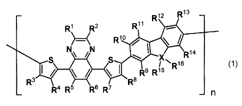
[Formula 1]
¨ R12 R13 ¨
R1 R2 R11
N\ /N
Rlo
)-----<
Ria
S S X
/ R16 (1)
1/ * \l R9 R15
R3 le
R4 R5 R6 R7
..... ¨n
wherein each of Rl and R2 that may be the same or
different represents an optionally substituted aryl group;
provided that when a substituent is present, the substituent is
an alkyl group having 1 to 3 carbon atoms, an alkoxy group
having 1 to 3 carbon atoms, an aryl group, a heteroaryl group,
or halogen; each of R3 through RN that may be the same or
different represents hydrogen, an alkyl group, an alkoxy group,
an aryl group, an heteroaryl group, or halogen; each of R15 and
R1-6 that may be the same or different represents an alkyl group
having 6 or more carbon atoms; X represents carbon, nitrogen or
silicon; in the case where X is nitrogen, no R16 exists; and n
represents a range from 10 or more to 1000 or less.
CA 02749060 2016-04-25
76199-325
7a
EFFECTS OF THE INVENTION
[0011]
In accordance with the material for a photovoltaic device
of the present invention, it is possible to provide a
photovoltaic device having a high photoelectric conversion
efficiency.
BRIEF DESCRIPTION OF THE DRAWINGS
[0012]
Fig. 1 is a schematic drawing that shows one aspect of a
photovoltaic device in accordance with the present invention.
Fig. 2 is a schematic drawing that shows another aspect of
the photovoltaic device of the present invention.
Fig. 3 illustrates an ultraviolet-ray visible absorption
spectrum of a thin film ( film thickness: about 60nm) of compound
A-1.
Fig. 4 illustrates an ultraviolet-ray visible absorption
spectrum of a thin film ( film thickness : about 60nm) of compound
B-1.
Fig. 5 illustrates current-voltage characteristics of
example 1.
Fig. 6 illustrates current-voltage characteristics of
CA 02749060 2011-07-06
8
example 2.
Fig. 7 illustrates current-voltage characteristics of
example 3.
Fig. 8 illustrates current-voltage characteristics of
example 4.
Fig. 9 illustrates current-voltage characteristics of
example 5.
Fig. 10 illustrates current-voltage characteristics of
example 6.
Fig. 11 illustrates current-voltage characteristics of
example 7.
Fig. 12 illustrates current-voltage characteristics of
example 8.
Fig. 13 illustrates current-voltage characteristics of
example 9.
Fig. 14 illustrates current-voltage characteristics of
comparative example 1.
Fig. 15 illustrates current-voltage characteristics of
comparative example 2.
Fig. 16 illustrates current-voltage characteristics of
example 10.
Fig. 17 illustrates current-voltage characteristics of
example 11.
Fig. 18 illustrates current-voltage characteristics of
example 12.
CA 02749060 2011-07-06
9
Fig. 19 illustrates current-voltage characteristics of
example 13.
Fig. 20 illustrates current-voltage characteristics of
example 14.
Fig. 21 illustrates current-voltage characteristics of
comparative example 3.
Fig. 22 illustrates current-voltage characteristics of
comparative example 4.
Fig. 23 illustrates current-voltage characteristics of
comparative example 5.
Fig. 24 illustrates an image of the surface status of an
organic semiconductor layer of example 1 analyzed by an atomic
force microscope (AFM).
Fig. 25 illustrates an image of the surface status of an
organic semiconductor layer of comparative example 1 analyzed
by an atomic force microscope (AFM).
Fig. 26 illustrates an external quantum efficiency (EQE)
spectrum of a photovoltaic device of example 10.
Fig. 27 is a schematic drawing of the photovoltaic device
of example 1.
MODE FOR CARRYING OUT THE INVENTION
[0013]
The material for a photovoltaic device of the present
invention contains an electron donating organic material having
CA 02749060 2011-07-06
a structure represented by the general formula (1).
[0014]
[Formula 1]
R
¨ R12 13 ¨
R1 R11
. =
R2
N\ /N R10
R14
S X, (1)
i'.'.
\ ________________ / \ I R9 R15
R8
R4 R5 R6 R7 -n
[0015]
Each of R1 and R2 that may be the same or different represents
an optionally substituted alkyl group having 1 to 5 carbon atoms,
an optionally substituted alkoxy group having 1 to 5 carbon
atoms, an optionally substituted aryl group, or an optionally
substituted heteroaryl group, provided that when a substituent
is present, the substituent is an alkyl group having 1 to 5 carbon
atoms, an alkoxy group having 1 to 5 carbon atoms, an aryl group,
a heteroaryl group, or halogen.
[0016]
Each of R3 through R14 that may be the same or different
represents hydrogen, an alkyl group, an alkoxy group, an aryl
group, a heteroaryl group, or halogen.
[0017]
Each of R15 and R16 that may be the same or different
represents an alkyl group having 6 or more carbon atoms. The
number of carbon atoms of the alkyl group is preferably set in
CA 02749060 2011-07-06
11
a range from 8 or more to 30 or less, from the viewpoint of
processability. Moreover, from the viewpoints of properly
maintaining the orientation of the main chain and of effectively
carrying out light absorption and carrier mobility, the number
thereof is preferably set to 20 or less, more preferably, to
or less.
[0018]
X represents carbon, nitrogen or silicon. In the case where
X is nitrogen, no R16 exists. Here, n represents a range from
10 or more to 1000 or less.
[0019]
Examples of the alkyl group herein include saturated
aliphatic hydrocarbon groups, such as a methyl group, an ethyl
group, a propyl group, a butyl group, a pentyl group, a hexyl
group, a heptyl group, an octyl group, a nonyl group, a decyl
group, an undecyl group, and a dodecyl group, and these may be
straight, branched, or cyclic, and may be unsubstituted or
substituted. The number of carbon atoms of the alkyl group is
preferably set in a range from 1 or more to 20 or less, from
the viewpoint of processability. When a substituent is present,
examples thereof include the following alkoxy group, aryl group,
heteroaryl group, and halogen. In the case where R1 and R2 are
substituted, examples of the substituent include the following
alkoxy group having 1 to 5 carbon atoms, aryl group, heteroaryl
group, and halogen.
CA 02749060 2011-07-06
12
[0020]
Moreover, the alkoxy group, for example, represents an
aliphatic hydrocarbon group with an ether bond, such as a
methoxy group, an ethoxy group, a propoxy group, and a butoxy
group, and the aliphatic hydrocarbon group may be unsubstituted
or substituted. The number of carbon atoms of the alkoxy group
is preferably set in a range from 1 or more to 20 or less, from
the viewpoint of precessability. . When a substituent is present,
examples thereof include the following aryl group, heteroaryl
group, and halogen. Herein, in the case where Rl and R2 are
substituted, examples of the substituent include the following
aryl group, heteroaryl group, and halogen.
[0021]
Examples of the aryl group include aromatic hydrocarbon
groups, such as a phenyl group, a naphthyl group, a biphenyl
group, a phenanthryl group, an anthryl group, a terphenyl group,
a pyrenyl group, a fluorenyl group, and a perylenyl group, and
these may be unsubstituted or substituted. The number of carbon
atoms of the aryl group is preferably set in a range from 6 or
more to 30 or less, from the viewpoint of processability. When
a substituent is present, examples thereof include the
above-mentioned alkyl group, the following heteroaryl group,
and halogen. In the case where Rl and R2 are substituted,
examples of the substituent include the above-mentioned alkyl
group having 1 to 5 carbon atoms, and alkoxy group having 1 to
CA 02749060 2011-07-06
13
carbon atoms, and the following heteroaryl group, or halogen.
[0022]
The heteroaryl group represents, for example, a
heteroaromatic group having atoms other than carbon atoms, such
as a thienyl group, a furyl group, a pyrrolyl group, an
imidazolyl group, a pyrazolyl group, an oxazolyl group, a
pyridyl group, a pyrazyl group, a pyrimidyl group, a quinolinyl
group, an isoquinolinyl group, a quinoxalinyl group, an
acridinyl group, an indolyl group, a carbazolyl group, a
benzofuran group, a dibenzofuran group, a benzothiophene group,
a dibenzothiophene group, a silole group, a benzosilole group,
and a dibenzosilole group, and these groups may be unsubstituted
or substituted. The number of carbon atoms of the heteroaryl
group is preferably set in a range from 3 or more to 30 or less,
from the viewpoint of processability. When a substituent is
present, examples thereof include the above-mentioned alkyl
group, aryl group, and the following halogen. In the case where
R1 and R2 are substituted, examples of the substituent include
the above-mentioned alkyl group having 1 to 5 carbon atoms,
alkoxy group having 1 to 5 carbon atoms, aryl group, or halogen.
Moreover, the halogen is at least any one selected from fluorine,
chlorine, bromine, and iodine.
[0023]
In the general formula (1) , n represents a degree of
polymerization, which is set in a range .from 10 or more to 1000
CA 02749060 2011-07-06
14
or less. The degree of polymerization can be determined from
the weight-average molecular weight. The weight-average
molecular weight is measured by using a GPC (gel permeation
chromatography), and can be converted based upon polystyrene
standard sample.
[0024]
In most cases, the photoelectric conversion efficiency of
a photovoltaic device shows a correlation with the molecular
weight of an electron donating organic material. In order to
obtain a high photoelectric conversion efficiency, a conjugated
polymer having a number-average molecular weight of 5000 or more,
more preferably, 10000 or more, is desirably used as the
electron donating organic material. However, since the
conjugated polymer generally has a rigid main chain, its
solubility is low, and in order to obtain such a polymer having
a high molecular weight and high solubility, it is generally
considered that an alkyl group having 6 or more carbon atoms,
or an alkoxy group having 6 or more carbon atoms needs to be
introduced as a solubilizing group. As a specific example of
such a polymer, Poly(3-hexylthiophene), and APFO-15, which is
described in "Advanced Functional Materials", pages 3836-3842,
Volume 17, 2007, have been proposed. On the other hand, as a
method for improving the photoelectric conversion efficiency
from the viewpoint of its device structure, a bulk
hetero-junction-type photovoltaic device, which increases the
CA 02749060 2011-07-06
junction surface that devotes to photoelectric conversion by
mixing an electron accepting organic material and an electron
donating with each other, has been known. In the bulk
hetero-junction-type photovoltaic device, the electron
donating organic material and the electron accepting organic
material are preferably phase-separated from each other in a
nano-level, without being completely compatible with each other,
so as to form a passing route (carrier path) for electrons and
holes. However, the solubilizing group, which has been
introduced so as to increase the solubility of the electron
= donating organic material as described above, tends to increase
the compatibility with the electron accepting organic material
to impair the formation of a phase-separated structure, or, in
contrast, lower the compatibility with the electron donating
organic material to cause a phase separation in a micrometer
scale, with the result that the bulk hetero-junction-type
photovoltaic device is not allowed to exert the photoelectric
conversion effect sufficiently.
[0025]
In this manner, it has been difficult to satisfy both of
functions for providing a high molecular weight, while
maintaining sufficient solubility, and for providing a
capability of forming a phase-separated structure that is
suitable for the bulk hetero-junction-type photovoltaic
device; however, the electron donating organic material having
CA 02749060 2011-07-06
=
16
a structure represented by the general formula (1) of the
present invention makes it possible to achieve both of the
functions.
[0026]
The electron donating organic material having a structure
represented by the general formula (1) forms a main-chain
structure constituted by a quinoxaline skeleton having the
substituents Rl and R2, two thiophene skeletons disposed on the
two sides of this quinoxaline skeleton, and a divalent linking
group (fluorine, silafluorene, or carbazole) that links triads
of the thiophene-quinoxaline-thiophene to one after another.
[0027]
The quinoxaline skeleton forming a first constituent
element tends to cause an aggregation due to it-it stacking since
its planarity is high, and is considered to easily form a
phase-separation structure that is suitable for the
above-mentioned bulk hetero-junction. However, in the case
where none of the substituents Rl and R2 are placed, since the
chemical stability of the electron donating organic material
is low and the aggregating force is too high, an excessive
crystallization is caused to result in a reduction in the
photoelectric conversion efficiency of the photovoltaic device.
In contrast, in the case where a solubilizing group, such as
an alkyl group having 6 or more carbon atoms and an alkoxy group
having 6 or more carbon atoms, is located at each of the positions
CA 02749060 2011-07-06
17
of Rl and R2, since, as described above, the compatibility with
the electron accepting organic material is increased to impair
the formation of the phase separation structure, or, in contrast,
the compatibility with the electron accepting organic material
is lowered to cause a phase separation in a micrometer scale,
it becomes difficult to form a phase separation structure that
is desirable for.a bulk hetero-junction-type photovoltaic
device, thereby failing to sufficiently exert the photoelectric
conversion efficiency. In order to ensure such chemical
stability and suitable phase-separation structure forming
capability, it has been found that it is very effective that
the substituent at each of the positions of Rl and R2 is an
optionally substituted alkyl group having 1 to 5 carbon atoms,
an optionally substituted alkoxy group having 1 to 5 carbon
atoms, an optionally substituted aryl group, or an optionally
substituted hetero-aryl group, and that when a substituent is
present, it is an alkyl group having 1 to 5 carbon atoms, an
alkoxy group having 1 to 5 carbon atoms, an aryl group, a
hetero-aryl group, or halogen.
[0028]
In the case where the thiophene skeleton serving as the
second constituent element is allowed to form the triads of the
thiophene-quinoxaline-thiophene in combination with the
quinoxaline skeleton, the band gap of the main chain skeleton
is lowered so as to devote to an increase of a short-circuit
CA 02749060 2011-07-06
18
current (Jsc) of the photovoltaic device. The number of the
thiophene rings needs to be set so that one ring is placed on
each of the two sides of the quinoxaline skeleton. When two
of these are placed on each of the sides, the solubility is
lowered to cause an extreme reduction of synthesis yield, or
the thiophene rings are mutually twisted to sometimes impair
the carrier mobility.
[0029]
The divalent linking group (fluorine, silafluorene, or
carbazole) forming a third constituent element is a very
effective skeleton for providing a high molecular weight and
for forming a suitable phase separation structure in a
nano-level. These linking groups are characterized in that
these easily allow a solubilizing group required for providing
a high molecular weight to be synthetically introduced. What
is more important than this is that, in contrast to the fact
that, when introduced into the quinoxaline skeleton, a
solubilizing group having 6 or more carbon atoms intervenes with
the formation of a phase separation structure, a solubilizing
group (alkyl group), introduced into these divalent linking
group (fluorine, silafluorene, or carbazole), exerts such
effects that it becomes possible to accelerate to provide a high
molecular weight, and also to devote to the formation of a
suitable phase separation structure. It is unexpectedly found
that these peculiar effects can be exerted for the first time
CA 02749060 2011-07-06
19
when combined with the triad of the aforementioned
thiophene-quinoxaline-thiophene. Among these, fluorene is
superior in these effects, and this lies in that in the same
manner as in the fact that polyfluorene has a 13-phase forming
capability, when fluorene is used as its linking group, the
electron donating organic material having a structure
represented by the general formula (1) of the present invention
is allowed to easily form a peculiar aggregated structure.
[0030]
From the viewpoints of satisfying preparations of both of
a high molecular weight and a phase-separation-structure
forming capability, as well as easiness of synthesis and high
yield, among the above-mentioned substituents, R1 and R2 are
preferably optionally substituted aryl groups, and R3 to R14 are
more preferably hydrogen or aryl groups. In the case where R1
and R2 are substituted aryl groups, the substituent is
preferably an alkyl group having 1 to 5 carbon atoms or an alkoxy
group having 1 to 5 carbon atoms, and more preferably an alkyl
group having 1 to 3 carbon atoms or an alkoxy group having 1
to 3 carbon atoms.
[0031]
As the electron donating organic material having a
structure represented by the general formula (1) , the following
structures are proposed. In the following structures, n is set
in a range from 10 or more to 1000 or less.
CA 02749060 2011-07-06
.
,
[0032]
[Formula 2]
N` N ... Q.
Is/ 4P n S 400
I / 4,
\i
n
N"N 0.11
1/ * \I n
S 404.
I /
`1,1 ISO )r-e '
If . \I n ***
I, 1, \ n
-
Q
--..
1 * \I 4111. n S
I / . \ 41141" n
8
N"N 0111*. U
I, op , n 400 n
cI'p
0
N"N 40401
I! 11 \I n S N" ...
I / * \ I n
[0033]
[Formula 3]
,
CA 02749060 2011-07-06
. .
= 21
w Q
N N * = N' \N 40 g=
/ . o_ify
-
8
ftN"N
- I / . \ I/. S!k * =
I
si =
_ I S -,
I / Mr I/
_
N' \N 0 li= "N 0 *.
_ I / * 07i_ JL___\: I
8
N' \N0 * I N' \ /41 S4." - n
m--k
- I / . \ I ,r,L--
_rj - IS?
,
0;2? )
S N"N
- I / It \ 1/----N,N,_ - S p
I,
[0034]
[Formula 4]
CA 02749060 2011-07-06
,
22
\),----
N N 40 41 Q
"N 40 41
N
ii ..)
40 1 1/ 40 \I
N N 40 41
- Ii . \I U
' µ 40 4/
N\---\:_.;._
s
- 1,1
1 , # \i N,õ___\3.
,
N 0 = 1
- I / I /
tsk--N_-_,
= \ I - = \ I
_
-
Q
"N 40 41 _
, ,,,,, 40 4/
- I I
NN__
* \ - I / * \ I
-
U
i \ N Hi,,-
S
- p 0 41
s.__\___\___\___ n 1,ie \ 1 I , # \ I
,
I' 0
PN 40 41 '34)
Ni \
' Is, ilp 0 N\¨\...7_,_
- I s, = \ I
[0035]
[Formula 5]
CA 02749060 2011-07-06
. .
23
*1 *4
N N 400 N" 00
S n n
II 4 \I 1/ 4\. 1
*4 *4
N"N 400 N' 'N 40401
n n
1, 4 0 1/ * \I
*4 *4
N/ 'N 00 N' 'N 4040'
n
1/ 4 0 1/ * \I n
*4 *4
'N 00 "N 400
S n n
1/ * \I I, ip 0
F ei \=
. 0 = 0
"N 000N" 4040'
S n
1, ip 0 n 1/ * \I
If I/
*4 ml* .116
_.rn m
400 ¨N 1 ea,
n
1 / lik
\. 1 Sz * \S I "w" n
[0036]
[Formula 6]
CA 02749060 2011-07-06
24
*
*
N .10
I /
S ANL 40110
/ \
*
*
N 44411k
/ \ I
*OP
I = S n
*
N 4110 411
\ N"
I / \ I
N" *** *
I
I / =
\
*
it it
\ N 41110
/ \l
*
N
\ III
N" ***
I * \ I
[ 0 03 7
[Formula 7]
CA 02749060 2011-07-06
. ,
= 4* it 41
s Ni 'N SO N N 400
n S n
1 / 1, \I 1
1, 0 . =
S NAik' -'11 400 N' 'N 00
n n
I/ IF \I 1/ 4p 0
= It. If 41
N N Se* , \ 00
S n S NN
n
1/ II \ I I/ ir \I
ID ii it 0
rµil 'N SO N' 'el 400
n n
1/ it 0 I, 4, 0
F F el \e
N" OOP N" 0010
n n
I, 0 1/ 4P 1
,.
Ilk .
II = JO Om
N' 'IV 001 n "N alfie
1/ = \I i s/ . \S
41. l
[0038]
[Formula 8]
CA 02749060 2011-07-06
,
26
1, = - IP .
"N al 1,1 "N
_ IS/ . \ Illr _____N__I - I S/ * 0
. c. "N
- I/ ik \1 S
- I/
/
'N 0 =. "N a) ..
_ IS/ . \17__\._ _ I/
II iliit 41
S N"N 40 4A1 N"N 4 le.=1
- I/' \ liji _ S
I/
F 0i \ 0
* 410 II 410
_ S 10
I/ . -
- I/ lik
. 410
Ilk = lik 16
W W
N"
S
'' 40 1P1 N" 0 it
- I/ 1, \ I - - I/ *
[0039]
[Formula 9]
CA 02749060 2011-07-06
27
-*4*
s 'NI = Slit\N
- I/ IS/ \
#
\N * N" n
IS/ \ - I / \ I fri
*
N' 'NJ4 4 \N el
I / \ 171\--1
# #
= \N *I
I \I - I \
/
= =
=
\N It \N *
I \ I
41# #00,
N/ µN #1
- I \I IS/
[0040]
[Formula 101
CA 02749060 2011-07-06
,
28
.4
S -- .!n "N
I / m p \ I
1\--\---- _ S
I / le \ 17/"='"" 1,7\___:\___I
.4 - . =
S ' \N 0 g
I / 41) \ lyi5J---(\:__1 _ S N/ S 4 4 1
I / 11 \ 1/.....
44 -.4 _
' \N 0 4N' \N 4 4
\ .
I / 4I
k______..I - I / 4 \ I-(\
- 4 4 - 4 411
N"N 4 4
S ./-.k N' \N 4 4
I / lir \ I,/k.-.\;.1 L I S
_ / it \ 1/--(\
F
s/ \=
r 4 0 4 4
N" 44 _______________________________ 14 4
_ I 5/4 \ I$ iµ_..\__i ...,
.¨ S
I / IIP \ I i n
Ilik 41
- 4, _
. N'' 0 4- 4D4 441
N'' at it
I , 4 , 1_4 .-j,...i
- I , 4 , I,/1._
[0041]
[Formula 11]
,
CA 02749060 2011-07-06
. .
29
*1
"N40 It 40 it .
S N1
_ 1 S/ = \i N.,___\s_:L_\__
- I / * \ I
- # 6
N' \N =N' S
N 0 *
.
_ 1 S/ * \ 1 ,\.:._
N-r,____ ,
I / * I
S Aa 411 N411) is( \N 00 = 1
I / V \ I n
- I /
r 4). 41 ,
N' \N
4 NIP 1 n N"N 0 #
_ S p
S p
I / V \ I
F i \
#=
- # = - 4
L S S 10 ' \N = *
I, it 0 --\--\_\_ I s, = , I N......_\,..,1
# *
'4
N" 0 = 1
N n N' \N 410 = 1
, I S/ 4 \ I
_
µ--\---\---\____ \ .
I / * I
[0042]
[Formula 12]
CA 02749060 2011-07-06
-.4
Ni 'N ___ 4it ]
i n
_ S N N 0 4
1 / IP \ I N n
-
44 - 4,
N/ 'N 4 4 n
I / 4 1 -
\ . SO
I, 4 \I n
-.4 _ 4,
N' 'N 04 N N 01 4
- 1 / 4 1
S
\ . N _ n
I / 4 i
-.4-4,
N" 01 4 N' 'N 0 4 ]
- '/
N n
1, 4 \I
.
i \
F s
S
4,
N" 0 4
I / 4 \ I n
- I, 4 \I
It AO'
- lik 4 0 Ai
_ s N" 0 4
I, 4 1
\. N _ n N' N 0 4
- 1 / 11
[0043]
[Formula 13]
CA 02749060 2011-07-06
. .
31
\ / 1110' N\---/ 'N
4. ¨
dim&
S "N S S.
MIP"'w n
n S
1, 4 0 1, 4 0
*5
S N',.; SO S N" 00
n n
I / w \ II
\
I / 4,
p.
40 40
= = *4_ _
s N/ \N 00 N" ***
n n
1, 4 0 I , 4 ,s 1
40111 40
. 410
*4 / * 4 \
s N',..- ea*
w.--, n S dilli,
'11-1"w n
I/ Mr \I I/ II \I
0 * N\
ar - - \ , 0
N" ea.
n
\ .
1, 4 1 1/ 40 0
, ,
IC
N/ \ N
-* 00 n \--N , \ N-
S N 5*
I Si * \I
I, 4 \I n
[0044]
[ Formula 14]
CA 02749060 2011-07-06
32
*
N .1101 *
/ = s N"N 1110
I / ,
\
*
.110 *
I / z N
I ,
=\ ,
*
N *110 *
I *
N"N ***
I /
\
*4
*4
= *
e 1101
1/
1 *
=
(?\
# ei
N" *
I / 4111,
\ 4114)
I,
\ ***
*
\
0,10 *.
,
\
*110
1 /
\I
10045]
[Formula 15]
CA 02749060 2011-07-06
33
410 = II
N' SIP N"
I/ = \I I/ I
= # =
0010
/ = \ I, =
#
N/ ONO "N **#
/
1/= \
N" 011# n \n/ OOP n
/ \ I, 4\I
9
(?,
=
# # =
Se*n N/ **#
S/
/ \
# *#
N/ ISO 40 n
1/ 4P \I Is/ 4P 1
[0046]
[Formula 16]
CA 02749060 2011-07-06
,
34 =
- * . '4
al ________________
N"N I=
* L N " 0 *
."`"I' Si
_I,.
\ v. ,, 4 \, si,
.4 *0
... N"N al 4I / * \ I I
\ 1 / ik \ 1
,
.4 .4
'N gl *.
N' \N 0 ,
I / 4 \S I '`,1." k__\...._t_\__I
\I / 4 \ I
.4 .4
* 11) / %
\ I # \ I = k---\_.-N \__n
e # \ I 4 4
= / I /
F =/ \=
= = - = =
N" = *. 1 0 li. 1
,
_ S
I / 4 , 1\\ _ 1 s/ 4 \ 1 L__,\_____,_
= 4
44 m= Am
w .._
0 4) 0 IP
I si * \ 1 ___\_i 1 , 4 , I
[0047]
[Formula 17]
,
CA 02749060 2011-07-06
,
,
NI' \ SO N' \ 400
n n
t/ la \I I, . \ I
F F CI CI
* . '4
N' ' 00 IA' 'N 00
n
I! = \i I / * n
F3C CF3 F F
*1 \*
'4 = .
S S ISO n N' 'N
1 / * \ I! * n
F F
F F
F
.4 .4
... N"N 40
n
1/ 4\ I I, 4\S I n
F F
F F
' * . '4 _
_ N" il , N"N * *
- 1 bi 4I '','" I /
F F
F F
44 -
N"4, "N
S S 41 N n ________________________ 0 11 i
I / 4 \ I - I S/ 4 \ 1 14,..,,,\ =
F F F F
[0048]
[Formula 18]
CA 02749060 2011-07-06
,
,
36
.4 . 0
.
S N' 'N 40 N/ \N 00
S n ,
n
I! \ I 1/ li
*4 *4
N"N 40 / 'N 40
n
I, 4p 0 I, 4/ 0 n
*4 .4
N"N SO
S N' 'N
410
n
I, 4/ 0 I, 4/ 0 n
*4 *4
N' \ 40 ' 'N 40)
n n
1/ . \ I I / . \ I
\
F = =
igikti
N/ a
N Wu.4/
s ww r, s u' n
I! . \I 1/ * \ I
1 4
*4 A 1. 4/ k
W W
N" 004, 4,0
n
1/ . \I S n
1/ . I
\.
[0049]
The electron donating organic material having a structure
CA 02749060 2016-04-25
76199-325
37
represented by the general formula (1) can be synthesized by, for
example, a technique similar to the method described in
A. Gadisa, W. Mammo, L. M. Andersson, S. Admassie, F. Zhang,
M.R. Andersson, and 0. Inganas, "Advanced Functional Materials",
pages 3836-3842, Volume 17, 2007.
[0050]
The material for a photovoltaic device of the present
invention may be made from only the electron donating organic
material having a structure represented by the general formula
(1), or may contain another electron donating organic material.
As the other electron donating organic material, examples
thereof include conjugated polymers, such as a polythiophene
polymer, a poly-p-phenylenevinylene copolymer, a
poly-p-phenylene polymer, a polyfluorene polymer, a
polypyrrole polymer, a polyaniline polymer, a polyacetylene
polymer, and a polythienylene vinylene polymer, and
low-molecular weight organic compounds including
phthalocyanine derivatives, such as H2 phthalocyanine (H2Pc),
cupper phthalocyanine (CuPc), and zinc phthalocyanine (ZnPc),
porphyrin derivatives, triaryl amine derivatives, such as
N,N'-diphenyl-N,N'-di(3-methylpheny1)-4,4'-dipheny1-1,1'-di
amine (TED) and
N,N'-dinaphtyl-N,N'-dipheny1-4,4'-dipheny1-1,1'-diamine
(NPD), carbazole derivatives, such as 4,4'-di(carbazole-9-y1)
biphenyl (CBE), and oligothiophene,derivatives (terthiophehe,
quaterthiophene, sexithiophene, octithiophene, etc.).
[0051]
CA 02749060 2011-07-06
,
38
Since the electron donating organic material having a
structure represented by the general formula (1) exerts a p-type
semiconductor characteristic, it is preferable to combine it
with an electron accepting organic material (n-type organic
semiconductor) in order to obtain a higher photoelectric
conversion efficiency, when used for a photovoltaic device.
[0052]
The electron accepting organic material corresponds to an
organic material that exerts an n-type semiconductor
characteristic, and examples thereof include: oxazole
derivatives, such as 1,4,5,8-naphthalene tetracarboxylic
dianhydride (NTCDA), 3,4,9,10-perylenetetracarboxylic
dianhydride (PTCDA), 3,4,9,10-perylenetetracarboxylic
bisbenzimidazole (PTCBI),
N,N'-diocty1-3,4,9,10-naphthyltetracarboxy diimide
(PTCDI-C8H),
2-(4-biphenyl)-5-(4-t-butylpheny1)-1,3,4-oxadiazole (PBD),
2,5-di(1-naphthyl)-1,3,4-oxadiazole (BND); triazole
derivatives, such as
3-(4-bepheny1)-4-pheny1-5-(4-t-butylpheny1)-1,2,4-triazole
(TAZ); phenanthroline derivatives, phosphine oxide
derivatives, fullerene compounds, carbon nano-tubes (CNT), and
a derivative (CN-PPV) prepared by introducing a cyano group to
a poly-p-phenylenevinylene polymer. Among these, the
fullerene compound is desirably used because it has high charge
CA 02749060 2011-07-06
39
separating rate and electron mobility. Examples of the
fullerene compounds include: unsubstituted compounds
including CH, C70, C76, C79, C82, C84, CH and C94, [6,6]-phenyl
C61 butyric acid methyl ester ([6,6]-PCBM), [5,6]-phenyl C61
butyric acid methyl ester ([5,6]-PCBM), [6,6]-phenyl C61
butyric acid hexyl ester ( [6, 6] -PCBH) , [6, 6] -phenyl C61 butyric
acid dodecyl ester ( [6, 6] -PCBD) , phenyl C71 butyric acid methyl
ester (PC70BM), and phenyl C85 butyric acid methyl ester (PC84BM).
Among the fullerene compounds, the C70 derivative (the
above-mentioned PC70BM or the like) is preferably used because
it is superior in light absorbing characteristic, and provides
a higher photoelectric conversion efficiency.
[0053]
In the material for a photovoltaic device of the present
invention, although not particularly limited, the content ratio
(weight percentage) of the electron donating organic material
and the electron accepting organic material is preferably set
in a range from 1 to 99 : 99 to 1, more preferably, from 10 to
90 : 90 to 10, and most preferably, from 20 to 60 : 80 to 40,
in the weight percentage of the electron donating organic
material : the electron accepting organic material. The
electron donating organic material and the electron accepting
organic material are desirably used in a mixed state. As the
mixing method, although not particularly limited, a method is
proposed in which the electron donating organic material and
CA 02749060 2011-07-06
the electron accepting organic material are added to a solvent
at a desired ratio so as to be dissolved. Additionally, in the
case where the material for a photovoltaic device forms a single
organic semiconductor layer, as will be described later, the
above-mentioned content ratio refers to a content ratio of the
electron donating organic material and the electron accepting
organic material contained in the single layer. Moreover, in
the case of a stacked structure having two or more organic
semiconductor layers, the above-mentioned content ratio refers
to a content ratio of the electron donating organic material
and the electron accepting organic material in the entire
organic semiconductor layers.
[0054]
In order to further improve the photoelectric conversion
efficiency, it is preferable to eliminate impurities that might
cause a trap of carriers to be kept to a minimum. As the method
for eliminating impurities from the electron donating organic
material having a structure represented by the general formula
(1) and the electron accepting organic material, although not
particularly limited, the following methods may be used: a
column chromatography method, a re-crystallizing method, a
sublimation method, a re-precipitation method, a Soxhlet
extraction method, a molecular cutoff method by using GPC (Gel
Permeation Chromatography), a filtration method, an ion
exchange method, a chelate method, and the like. In general,
CA 02749060 2011-07-06
41
upon refining a low-molecular-weight organic material, the
column chromatography method, re-crystallizing method, or
sublimation method is preferably used. In contrast, upon
refining a high-molecular-weight organic material, the
re-precipitation method, Soxhlet extraction method, molecular
cutoff method by using GPC (Gel Permeation Chromatography), or
filtration method is preferably used when a
low-molecular-weight component is eliminated, and the
re-precipitation method, chelate method, ion exchange method,
or column chromatography method is preferably used, when a metal
component is eliminated. Among these methods, a plurality of
methods may be combined.
[0055]
The following description will discuss the photovoltaic
device of the present invention. The photovoltaic device of
the present invention is provided with at least a positive
electrode and a negative electrode, and a layer containing the
material for a photovoltaic device of the present invention is
placed between the positive electrode and the negative
electrode. Fig. 1 is a schematic drawing that shows one example
of the photovoltaic device of the present invention. In Fig.
1, reference numeral 1 represents a substrate, reference
numeral 2 represents the positive electrode, reference numeral
3 represents an organic semiconductor layer containing the
material for a photovoltaic device of the present invention,
CA 02749060 2011-07-06
42
and reference numeral 4 represents the negative electrode.
[0056]
The organic semiconductor layer 3 contains the material for
a photovoltaic device of the present invention, that is, an
electron donating organic material having a structure
represented by the general formula (1). In the case where the
material for a photovoltaic device contains an electron
donating organic material and an electron accepting organic
material, these materials may be mixed with each other, or
formed as stacked layers; however, the mixed state is more
preferable. The aforementioned "bulk hetero-junction type"
refers to this mixed type. In the case of the mixed type, the
electron donating organic material having a structure
represented by the general formula (1) and the electron
accepting organic material are compatibly dissolved with each
other in a molecular level, or preferably phase-separated from
each other in a nano-level . In the case of the phase separation,
although not particularly limited, the domain size of the phase
separation structure is preferably set in a size from 1 nm or
more to 50 nm or less.
[0057]
In the case where the electron donating organic material
and the electron accepting organic material are stacked with
each other, the layer containing the electron donating organic
material that exhibits a p-type semiconductor characteristic
CA 02749060 2011-07-06
43
is preferably placed on the positive electrode side, while the
layer containing the electron accepting organic material that
exhibits an n-type semiconductor characteristic is preferably
placed on the negative electrode side. Fig. 2 illustrates one
example of the photovoltaic device having the stacked structure.
Reference numeral 5 represents a layer having the electron
donating organic material having a structure represented by the
general formula (1), and reference numeral 6 represents a layer
having the electron accepting organic material.
[0058]
The organic semiconductor layer is preferably designed to
have a thickness in a range from 5 nm to 500 nm, more preferably,
from 30 nm to 300 nm. In the case of the stacked structure of
the organic semiconductor layers, the layer containing the
electron donating organic material having a structure
represented by the general formula (1) is preferably designed
to have a thickness from 1 nm to 400 nm, more preferably, from
15 nm to 150 nm, within the thickness of the entire organic
semiconductor layers. Moreover, the layer containing the
electron accepting organic material is preferably designed to
have a thickness from 1 nm to 499 nm, more preferably, from 15
nm to 150 nm, within the thickness of the entire organic
semiconductor layers.
[0059]
Moreover, the organic semiconductor layer 3 may further
CA 02749060 2011-07-06
44
include an electron donating organic material (p-type organic
semiconductor) other than the electron donating organic
material having a structure represented by the general formula
(1) . As the electron donating organic material (p-type organic
semiconductor) to be used in this case, those materials
exemplified before may be used.
[0060]
In the photovoltaic device, either the positive electrode
2 or the negative 4 is preferably allowed to have a
light-transmitting property. The light-transmitting property
of the electrode is not particularly limited as long as it allows
incident light to reach the organic semiconductor layer 3 so
that an electromotive force is generated. In this case, the
light-transmitting property is indicated by a value determined
from [Transmitted Light Intensity (W/m2)/Incident Light
Intensity (W/m2)] x 100 (%). The thickness of the electrode
having a light-transmitting property is only necessary to be
set in such a range that provides a proper light-transmitting
property and conductivity, and although different depending on
the electrode materials, it is preferably set to 20 cm to 300
nm. Additionally, the other electrode is not necessarily
required to have a light-transmitting property as long as it .
has conductivity, and the thickness thereof is also not
particularly limited.
[0061]
CA 02749060 2011-07-06
As the electrode material, it is preferable to use a
conductive material having a high work function for one of the
electrodes and a conductive material having a low workfunction
for the other electrode. The electrode using the conductive
material having a high work function forms the positive
electrode. As the conductive material having a high work
function, in addition to metals, such as gold, platinum,
chromium and nickel, oxides of metals such as indium, tin, or
molybdenum having transparency, or composite metal oxides, such
as indium tin oxide (ITO) and indium zinc oxide (IZO), are
preferably used. In this case, the conductive material to be
used for the positive electrode 2 is preferably designed to be
ohmic contact to the organic semiconductor layer 3. Moreover,
as will be described later, in the case where a hole transporting
layer is formed between the positive electrode 2 and the organic
semiconductor layer 3, the conductive material to be used for
the positive electrode 2 is preferably designed to be ohmic
contact to the hole transporting layer.
[0062]
The electrode using the conductive material having a low
work function forms the negative electrode. As the conductive
material having a low work function, alkali metals and alkali
earth metals, more specifically, lithium, magnesium, calcium
and the like, are used. Further, tin, silver and aluminium are
also preferably used. Moreover, electrodes made from the
CA 02749060 2016-04-25
76199-325
46
above-mentioned metals and alloys and made from a stacked member
of the abovementioned metals may be preferably used. In this
case, the conductive material to be used for the negative
electrode 4 is preferably designed to be ohmic contact to the
organic semiconductor layer 3. Moreover, as will be described
later, in the case where an electron transporting layer is
formed between the negative electrode 4 and the organic
semiconductor layer 3, the conductive material to be used for
the positive electrode 2 is preferably designed to be ohmic
contact to the electron transporting layer. Moreover, by
introducing a metal fluoride, such as lithium fluoride and
cesium fluoride onto the interface of the negative electrode
4 and the electron transporting layer, it becomes possible to
improve the output electric current.
[0063]
Depending on the kinds and usages of the photoelectric
conversion material, the substrate 1 may be formed as a
substrate on which an electrode material and an organic
semiconductor layer can be stacked, for example, as a film or
a plate manufactured by using any method from an inorganic
material, such as non-alkali glass and quartz glass, or an
organic material, such as polyester, polycarbonate, polyolefin,
polyamide, polyimide, polyphenylene sulfide,. polyparaxylene,
an epoxy resin, and a fluorine-based resin. Moreover, in the
case where light is made incident on the substrate side, each
CA 02749060 2011-07-06
. .
47
of the above-mentioned substrates is preferably allowed to have
a light-transmitting property of about 80%.
[0064]
In the present invention, a hole transporting layer may be
provided between the positive electrode 2 and the organic
semiconductor layer 3. As a material used for forming the hole
transporting layer, a conductive polymer, such as a
polythiophene-based polymer, poly-p-phenylenevinylene-based
polymer, and a polyfluorene-based polymer, and a
low-molecular-weight organic compound that exerts a p-type
semiconductor characteristic, such as a phthalocyanine
derivative (H2Pc, CuPc, ZnPc, and the like) and a porphyrin
derivative, are preferably used. In particular, those
materials, prepared by adding polystyrene sulfonate (PSS) to
polyethylene dioxythiophene (PEDOT) and PEDOT serving as a
polythiophene-based polymer, are preferably used. The hole
transporting layer preferably has a thickness in a range from
nm to 600 nm, and more preferably, from 30 nm to 200 nm.
Moreover, the hole transporting layer is preferably treated by
a fluorous compound (an organic compound having one or more
fluorine atoms in its molecule) so that it becomes possible to
further improve the photoelectric conversion efficiency.
Examples of the fluorous compound include: benzotrifluoride,
hexafluorobenzene, 1,1,1,3,3,3-hexafluoro-2-propanol,
perfluorotoluene, perfluorodecalin, perfluorohexane, and
CA 02749060 2011-07-06
48
1H,1H,2H,2H-heptadecafluoro-l-decanol (F-decanol). More
preferably, benzotrifluoride, perfluorohexane, and F-decanol
can be used. As the treating method, a method in which, after
the fluorous compound has been preliminarily mixed with a
material used for forming a hole transporting layer, the hole
transporting layer is formed, and a method in which, after a
hole transporting layer is formed, the fluorous compound is made
in contact therewith (such as spin coating, dip coating, blade
coating, vapor deposition, and vapor treating methods) can be
exemplified.
[0065]
Moreover, in the photovoltaic device cf.-the present
invention, an electron transporting layer may be provided
between the organic semiconductor layer 3 and the negative
electrode 4. As the material used for forming the electron
transporting layer, although not particularly limited, a
compound that exerts an n-type semiconductor characteristic,
such as the aforementioned electron accepting organic materials
(NTCDA, PTCDA, PTCDI-C8H, an oxazole derivative, a triazole
derivative, a phenanthroline derivative, a phosphine oxide
derivative, a fullerene derivative, CNT, CN-PPV, etc.) and
titanium oxide, are preferably used. The thickness of the
electron transporting layer is preferably set in a range from
nm to 600 nm, and more preferably, from 30 nm to 200 nm.
[0066]
CA 02749060 2011-07-06
=
49
Moreover, as the photovoltaic device of the present
invention, two or more organic semiconductor layers may be
stacked (into a tandem structure) , with one or more intermediate
layers interposed therebetween, so that series junctions may
be formed. For example, the stacked layer structure includes:
substrate/positive electrode/first organic semiconductor
layer/intermediate electrode/ second organic semiconductor
layer/negative electrode. By using this stacked layer
structure, it becomes possible to improve an open circuit
voltage. Additionally, the aforementioned hole transporting
layer may be provided between the positive electrode and the
first organic semiconductor layer, as well as between the
intermediate electrode and the second organic semiconductor
layer, or the hole transporting layer may be provided between
the first organic semiconductor layer and the intermediate
electrode, as well as between the second organic semiconductor
layer and the negative electrode.
[0067]
In the case of such a stacked-layer structure, at least one
of the organic semiconductor layers is preferably designed to
contain the material for a photovoltaic device of the present
invention, while the other layers are preferably designed to
contain an electron donating organic material having a bandgap
different from that of the electron donating organic material
of the present invention so as not to lower a short-circuit
CA 02749060 2011-07-06
current. Examples of the electron donating organic material
include: conjugated polymers, such as a polythiophene polymer,
a poly-p-phenylene vinylene copolymer, a poly-p-phenylene
polymer, a polyfluorene polymer, a polypyrrole polymer, a
polyaniline polymer, a polyacetylene polymer, a polythienylene
vinylene polymer, and a benzothiadiazole polymer (for example,
PCPDTBT
(poly[2,6-(4,4-bis-(2-ethylhexyl)-4H-cyclopenta[2,1-b;3,4-b
']dithiophene)-alt-4,7-(2,1,3-benzothiadiazole)]), and
PSBTBT
(poly[(4,4-bis-(2-ethylhexyl)dithieno[3,2-b:2',3'-d]silole)
-2,6,-diyl-alt-(2,1,3-benzothiadiazole)-4,7-diy1]); and the
aforementioned low-molecular-weight organic compounds
including phthalocyanine derivatives such as H2 phthalocyanine
(H2Pc), cupper phthalocyanine (CuPc), and zinc phthalocyanine
(ZnPc), porphyrin derivatives, triaryl amine derivatives such
as
N,N'-diphenyl-N,N'-di(3-methylpheny1)-4,4'-dipheny1-1,1'-di
amine (TPD) and
N,N'-dinaphtyl-N,N'-dipheny1-4,4'-dipheny1-1,1'-diamine
(NPD), carbazole derivatives such as 4,4'-di(carbazole-9-y1)
biphenyl (CBP), and oligothiophene derivatives such as
terthiophene, quaterthiophene, sexithiophene, and
octithiophene. Moreover, as the material for the intermediate
electrode to be used in this case, those having high
CA 02749060 2011-07-06
51
conductivity are preferably used, and examples thereof include
the aforementioned metals, such as gold, platinum, chromium,
nickel, lithium, magnesium, calcium, tin, silver and aluminum;
oxides of metals such as indium, tin, molybdenum and titanium
having transparency; or composite metal oxides, such as indium
tin oxide (ITO) and indium zinc oxide (IZO) ; alloys made from
the above-mentioned metals and laminates of the above-mentioned
metals; and polyethylene dioxythiophene (PEDOT) and PEDOT to
which polystyrene sulfonate (PSS) is added. The intermediate
electrode is preferably allowed to have a light-transmitting
property, and even in the case of a material such as metal having
a low light-transmitting property, by making the film thickness
thinner, a sufficient light-transmitting property can be
ensured in many cases.
[0068]
Moreover, the photovoltaic device of the present invention
may contain a pigment between the positive electrode and the
negative electrode. The pigment may be either luminescent or
non-luminescent. In the case of the luminous pigment, it may
be either fluorescent or phosphorescent. In this case,
fluorescence refers to a light emission caused by a transition
between states having the same spin multiplicity, and
phosphorescence refers to a light emission cause by a transition
between states that are different in spin multiplicity. For
example, luminescence caused by a transition from a singlet
CA 02749060 2011-07-06
52
excited state to the ground state (in general, the ground state
of an organic compound is singlet) is fluorescence, and
luminescence caused by a transition from a triplet excited state
to the ground state is phosphorescence. By allowing the element
to contain such a pigment, its light absorption can be increased,
or light having such short wavelengths that the electron
donating organic material and the electron accepting organic
material hardly absorb can be wavelength-converted to light
having long wavelengths that are easily absorbed so that it
becomes possible to improve a short-circuit current. From the
viewpoint of processability, the pigment is desirably an
organic pigment that is soluble to an organic solvent. Examples
of these organic pigments include: porphyrin derivatives,
phthalocyanine derivatives, naphthalocyanine derivatives,
coumarin derivatives, pyrromethene derivatives,
pyrrolopyrrole derivatives, anthracene derivatives, distyryl
benzene derivatives, tetraphenyl butadiene derivatives,
stilbene derivatives, phthalimide derivatives, naphthalimide
derivatives, perinone derivatives, cyclopentadiene
derivatives, acridone derivatives, quinacridone derivatives,
rare-earth complexes, such as an Eu complex having a ligand,
such as acetylacetone, benzoylacetone, phenanthroline, or the
like,
4-(dicyanomethylene)-2-methy1-6-(p-dimethylaminostyry1)-4H-
pyrane derivative, rhodamine compounds, deazaflavin
CA 02749060 2011-07-06
53
derivatives, phenoxazine derivatives, oxazine derivatives,
quinazoline derivatives, squarylium derivatives, violanthrone
derivatives, phenazine derivatives, phenoxazone derivatives,
and thiadiazolopyrene derivatives. The pigment may be stacked
between the positive electrode and the negative electrode, or
may be mixed in a layer selected from the organic semiconductor
layer, the hole transporting layer, and the electron
transporting layer. In order to exert the light absorbing
increasing effect and the wavelength converting effect, the
pigment is desirably mixed into the organic semiconductor
layer.
[0069]
The following description will discuss a method for
manufacturing the photovoltaic device of the present invention
based upon examples. A transparent electrode (corresponding
to a positive electrode in this case) made of ITO is formed on
a substrate by using a sputtering method or the like. Next,
a solution, prepared by dissolving an electron donating organic
material having a structure represented by the general formula
(1) and a material for a photovoltaic device containing an
electron accepting organic material, if necessary, in a solvent,
is applied to the transparent electrode so that an organic
semiconductor layer is formed. The solvent to be used at this
time is preferably an organic solvent. Examples thereof
include: methanol, ethanol, butanol, toluene, xylene,
CA 02749060 2011-07-06
54
o-chlorophenol, acetone, ethylacetate, ethylene glycol,
tetrahydrofuran, dichloromethane, chloroform, dichloroethane,
chlorobenzene, dichlorobenzene, trichlorobenzene,
chloronaphthalene, dimethylformamide, dimethylsolfoxide,
N-methylpyrrolidone and y-butyrolactone. Two or more kinds of
these may be used. Moreover, by allowing the solvent to contain
the aforementioned fluorous compound, the photoelectric
conversion efficiency can be further improved. Fluorous
compounds (fluorous solvents) in a liquid state under normal
temperature and normal pressure are preferably used, and, more
preferably, benzotrifluoride, perfluorohexane, or F-decanol
is used. The content of the fluorous compound is preferably
set to 0.01 to 20% by volume, and more preferably, to 0.1 to
2% by volume, relative to the total amount of the solvent. The
content of the fluorous solvent is preferably set to 0.01 to
30% by weight, and more preferably, to 0.1 to 4% by weight,
relative to the total amount of the solvent.
[0070]
In the case of mixing the electron donating organic material
having a structure represented by the general formula (1) and
the electron accepting organic material so as to form an organic
semiconductor layer, the electron donating organic material
having a structure represented by the general formula (1) and
the electron accepting organic material are added to a solvent
at the desired ratio, and by dissolving these by using a method
CA 02749060 2011-07-06
such as, heating, stirring, or irradiating with ultrasonic wave,
the resulting solution is applied onto the transparent
electrode.
[0071]
In this case, by using two or more kinds of the solvents
in a mixed manner, the photoelectric conversion efficiency of
the photovoltaic device can be improved. This effect is
presumably obtained by the fact that the electron donating
organic material and the electron accepting organic material
are phase-separated in a nano-level so that a carrier path that
forms a passing route of electrons and holes is formed. The
solvent to be combined therewith can be selected as an optimal
combination depending on the kinds of the electron donating
organic materials and the electron accepting organic materials.
In the case where the electron donating organic material having
a structure represented by the general formula (1) is used, a
combination between chloroform and chlorobenzene is
exemplified as a desired solvent. In this case, the mixed
volume ratio of the respective solvents is preferably set in
a range from 5 : 95 to 95 : 5 = chloroform : chlorobenzene, more
preferably, from 10 : 90 to 90 : 10 =chloroform: chlorobenzene.
[0072]
Moreover, in the case where the electron donating organic
material having a structure represented by the general formula
(1) and the electron accepting organic material are stacked so
CA 02749060 2011-07-06
56
as to form an organic semiconductor layer, for example, after
the solution of the electron donating organic material is
applied to form a layer having the electron donating organic
material thereon, a solution of the electron accepting organic
material is applied thereto so that a layer is formed. In the
case where each of the electron donating organic material and
the electron accepting organic material is a
low-molecular-weight substance whose molecular weight is about
1000 or less, the layer may be formed by using a vapor deposition
method.
[0073]
The organic semiconductor layer may be formed by using any
of the following application methods: a spin coating method,
a blade coating method, a slit die coating method, a screen
printing method, a bar coating method, a mold coating method,
a print transfer method, a dip coating method, an ink-jet method,
a spraying method, a vacuum vapor deposition method, and the
like. The formation method may be properly selected depending
on the characteristics of an organic semiconductor layer to be
obtained, such as film-thickness controlling and orientation
controlling. For example, in the case of carrying out the spin
coating method, the total amount of the electron donating
organic material having a structure represented by the general
formula (1) and the electron accepting organic material is
preferably set to 1 to 20 g/1 relative to the entire solution.
CA 02749060 2011-07-06
57
By using this concentration, a uniform organic semiconductor
layer with a thickness in a range from 5 to 200 nm can be easily
obtained. In order to remove the solvent, the organic
semiconductor layer thus formed may be subj ected to an annealing
treatment under reduced pressure or in an inert gas atmosphere
(in a nitrogen or argon atmosphere). The temperature of the
annealing treatment is preferably set in a range from 40 C to
300 C, more preferably, from 50 C to 200 C. By carrying out the
annealing treatment, the stacked layers are mutually allowed
to permeate each other through the interface, and the effective
contact areas consequently increase so that a short-circuit
current can be increased. This annealing treatment may be
carried out after the formation of the negative electrode.
[0074]
Next, a metal electrode (corresponding to a negative
electrode, in this case) made of Al is formed on the organic
semiconductor layer by a vacuum vapor deposition method, a
sputtering method, or the like. In the case where an electron
transporting layer is formed by the vacuum vapor deposition by
using a low-molecular-weight organic material as an electron
transporting layer, the metal electrode is preferably formed,
with the vacuum state being successively maintained.
[0075]
In the case where a hole transporting layer is provided
between the positive electrode and the organic semiconductor
CA 02749060 2011-07-06
58
layer, after a desired p-type organic semiconductor material
(PEDOT or the like) is applied on the positive electrode by a
spin coating method, a bar coating method, or a casting method
by the use of a blade, the solvent is removed by using a vacuum
thermostat, a hot plate, or the like so that the hole
transporting layer is formed. In the case where a
low-molecular-weight organic material, such as a
phthalocyanine derivative and a porphyrin derivative, is used,
a vacuum vapor deposition method by the use of a vacuum vapor
deposition machine may be adopted.
[0076]
In the case where an electron transporting layer is provided
between the organic semiconductor layer and the negative
electrode, after a desired n-type organic semiconductor
material (a fullerene derivative or the like) or n-type
inorganic semiconductor material (titanium oxide gel or the
like) is applied onto the organic semiconductor layer by a spin
coating method, a bar coating method, a casting method by the
use of a blade, a spraying method, or the like, the solvent is
removed by using a vacuum thermostat, a hot plate, or the like
so that the electron transporting layer is formed. In the case
where a low-molecular-weight organic material, such as a
phenanthroline derivative and 060, is used, a vacuum vapor
deposition method by the use of a vacuum vapor deposition
machine may be adopted.
CA 02749060 2011-07-06
59
[0077]
The photovoltaic device of the present invention may be
applicable to various photoelectric conversion devices in which
its photoelectric conversion function, photo-rectifying
function, or the like is utilized. For example, it is useful
for photoelectric cells (solar cells, or the like), electron
devices (a photosensor, photoswitch, phototransistor,
photoconductor, or the like), photorecording materials
(photomemory or the like).
EXAMPLES
[0078]
The following description will further discuss the present
invention based upon examples more specifically. Incidentally,
the present invention is not intended to be limited by the
following examples. Also, among compounds that are used in the
examples, those indicated by abbreviations are shown below.
ITO: Indium tin oxide
PEDOT: Polyethylene dioxythiophene
PSS: Polystyrene sulfonate
PC70BM: Phenyl C71 butyric acid methyl ester
Eg: Bandgap
HOMO: Highest occupied molecular orbital
Isc: Short-circuit current density
Voc: Open-circuit voltage
CA 02749060 2011-07-06
FF: Fill factor
Photoelectric conversion efficiency
Additionally, for 'H-NM R measurements, an FT-NMR analyzer
(JNM-EX270, made by JEOL Ltd.) was used. The average molecular
weight (number-average molecular weight, weight-average
molecular weight) was measured by GPC analyzer (high-speed GPC
device HLC-8220GPC with transported chloroform, made by Tosoh
Corporation), and calculated by an absolute calibration curve
method. The polymerization degree n was calculated based upon
the following expression:
Polymerization degree n = [(Weight-average molecular
weight)/(Molecular weight of repetitive units)
Moreover, with respect to an optical absorption edge
wavelength, measurements were carried out on a thin film formed
on glass with a thickness of about 60 nm by using a U-3010-type
spectrophotometer manufactured by Hitachi, Ltd., and based upon
the ultraviolet and visible absorption spectrum of the thin film
(measured wavelength range: 300 to 900 nm), the corresponding
value was obtained. The band gap (Eg) was calculated from the
optical absorption edge wavelength based upon the following
expression. In this case, the thin film was formed by a spin
coating method by the use of chloroform as a solvent.
Eg (eV) = 1240/Light absorption edge wavelength (nm)
Furthermore, the highest occupied molecular orbital (HOMO)
level was measured on a thin film formed on an ITO glass with
CA 02749060 2011-07-06
61
a thickness of about 60 nm, by using a surface analyzing
apparatus (Model AC-2 atmospheric ultraviolet photoelectron
spectrometer, manufactured by Rikenkiki Co., Ltd.). In this
case, the thin film was formed by a spin coating method by the
use of chloroform as a solvent.
[0079]
Synthesis Example 1
Compound A-1 was synthesized by using a method indicated
by Scheme 1.
[0080]
[Formula 19]
C-) ¨
o o
= Q
' 00
n 1¨ 00
ri o
Ct S
a 'TJ = 0
li 0 i5.Sn(rIBu)3
¨
=
0
¨ S
I'l 48%HBr Br2 _7 S3_84 NaBH4 H2N NH2 MOH N
Pd(PPh3)2C1
ca.
2
rli a
_
Br r ¨ Br lit :r ____________________
Br¨O¨Br
^
=Et0H
CHCb THE
i--
0- 1
1-1 cii
o ¨ (1-a) (1-b) (1-
c) (1-d) (1-e)
1-- ,-.--,,-
Q., .
(D
n
co
¨ LQ
0
,,)
.
,
,Q ,--6--
.
- 1-1
0c7,
0 (1-g)
cm 0
¨ a
N.) i.)
11 .
0
1-1 c P ri(PP h3)4
H
O
(D - H
I
a Q_. NiEls r , K2C01 /¨
0
01 l
.,.3
1
a 7= 5- Br Br
Aliquat 336 n
___,..
0
(D L< I ? # = . . = I
c7)
0-= H DM F
o Toluene/I-120
t-)-= pc=
(1-f)
= 0
Di n
s-= Scheme 1 A-1
O CD
= (=-)
hi pi
CD H,
(-) I-1
(D Q.
1--= = CD
O (1-
Sli I-1
1- L.<
.
CA 02749060 2011-07-06
63.
Industries, Ltd.) were added to 48% hydrobromic acid (150 mL)
(produced by Wako Pure Chemical Industries, Ltd. ) , and this was
stirred at 120 C for 3 hours. After being cooled to room
temperature, the resulting solid was filtered by a glass filter,
and washed with water (1000 mL) and acetone (100 mL) . The
resulting solid was vacuum-dried at 60 C so that compound (1-b)
(6.72 g) was obtained.
[0082]
The above-mentioned compound (1-b) (5.56 g) was added to
180 mL of ethanol (produced by Wako Pure Chemical Industries,
Ltd. ) , and to this was added 13.2 g of NaBH4 (produced by Wako
Pure Chemical Industries, Ltd.) at 5 C in a nitrogen atmosphere,
and then stirred at room temperature for 2 days. After the
solvent was distilled off, to this was added water (500 mL) so
that a solid was filtered and taken out, and washed with 1000
mL of water. The resulting solid was dissolved in 200 mL of
diethyl ether, and after being washed with water (300 mL) , this
was dried over magnesium sulfate. The solvent was distilled
off so that compound (1-c) (2.37 g) was obtained.
[0083]
The above-mentioned/compound (1-c) (2.37 g) and benzil
(1.87 g) (produced by Wako Pure Chemical Industries, Ltd.) were
added to 80 mL of chloroform, and after 3 drops of methane
sulfonic acid (produced by Wako Pure Chemical Industries, Ltd.)
was added thereto in a nitrogen atmosphere, this was heated and
CA 02749060 2011-07-06
64
refluxed for 11 hours. After the resulting solution was washed
with an aqueous sodium hydrogencarbonate solution, this was
dried over magnesium sulfate. The resulting solution was
purified by column chromatography (filler: silica gel, eluent:
chloroform), and washed with methanol so that compound (1-d)
(3.72 g) was obtained.
[0084]
The above-mentioned compound (1-d) (1.0 g) and
tributy1(2-thienyl)tin (1.87 g) (produced by Tokyo Chemical
Industry Co., Ltd.) were added to 20 mL of tetrahydrofuran
(produced by Wako Pure Chemical Industries, Ltd.), and to this
was added bis (triphenyl phosphine) palladium dichloride (32 mg)
(produced by Tokyo Chemical Industry Co., Ltd.) in a nitrogen
atmosphere, and heated and refluxed for 5 hours. After being
cooled to room temperature, to this was added methanol (50 mL)
and the resulting precipitate was filtered and taken out, and
then successively washed with methanol, water and methanol in
this order. The resulting solid was purified by column
chromatography (filler: silica gel, eluent: dichloromethane),
and washed with methanol so that compound (1-e) (693 mg) was
obtained.
[0085]
The above-mentioned compound (1-e) (693 mg) was dissolved
in dimethylformamide (80 mL) (produced by Wako Pure Chemical
Industries, Ltd.), and to this was added 550 mg of
CA 02749060 2016-04-25
76199-325
N-bromosuccinimide (produced by Wako Pure Chemical Industries,
Ltd.), and stirred at room temperature for 4 hours. Water (250
mL) was added to the resulting solution, and the resulting
precipitate was filtered and taken out, and then successively
washed with methanol and water in this order. The resulting
solid was purified by column chromatography (filler: silica gel,
eluent: dichloromethane), and washed with methanol so that
compound (1-f) (900 mg) was obtained. The result of 1H-NMR
= measurement on compound (1-f) is shown below:
1H-NMR (CDC13, ppm) : 8.10 (s, 2H), 7.72 - 7.69 (m, 4H), 7.59
(d, 2H), 7.43 - 7.41 (m, 6H), 7.13 (d, 2H).
[0086]
The above-mentioned compound (1-f) (330 mg) and compound
(1-g) described in formula 1 (304 mg) (produced by Aldrich
Corporation) were dissolved in 70 mL of toluene. To this were
added water (20 mL), potassium carbonate (1.51 g),
tetrakis(triphenylphosphine) palladium (0) (63 mg) (produced
TM
by Tokyo Chemical Industry Co., Ltd.), and 2 drops of Aliquat
336 (produced by Aldrich Corporation), and this was stirred at
100 C for 4.5 hours in a nitrogen atmosphere. Next, to this
was added 200 mg of bromobenzene (produced by Tokyo Chemical
Industry Co., Ltd.), and stirred at 100 C for one hour. Next,
to this was added 200 mg of phenylboronic acid (produced by Tokyo
Chemical Industry Co., Ltd.), and stirred at 100 C for 2 hours.
To the resulting solution was added 200 mL of methanol, and the
CA 02749060 2011-07-06
,
66
generated solid was filtered and taken out, and then washed with
methanol, acetone, water and acetone in this order. The
resulting solid was added to 300 mL of acetone, and heated and
refluxed for 30 minutes. The solid, obtained through
filtration while being heated, was dissolved in 300 mL of
chloroform, and after being filtered through a silica gel short
column (eluent: chloroform), the resulting solution was
condensed, and re-precipitated with methanol so that compound
A-1 (354 g) was obtained (yield: 78%). This compound had the
weight-average molecular weight of 39500, the number-average
molecular weight of 16600, and the degree of polymerization n
of 47.4% Moreover, the light absorption edge wavelength
thereof was 636nm, the bandgap (Eg) was 1. 95 eV, and the highest
occupied molecular orbital (HOMO) level was -5.37 eV.
[0087]
Synthesis Example 2
Compound A-2 was synthesized by using a method indicated
by Scheme 2.
[0088]
[Formula 20]
CA 02749060 2011-07-06
67
-C,
C.Igj
1111
CO
r-
M
Z a
1110
C a)
_e
-5 0_
cJ
a)
1¨
crb-_
cf)
6.
gt
Jc
o
0
Ef 6
0- 0
z u p 14.2-
<
qL-
cno
I'-
[0089]
Compound (1-c) (1.22 g) of synthesis example 1 and
4,4' -dimethoxybenzyl (1.24 g) (produced by Wako Pure Chemical
Industries, Ltd.) were added to chloroform (45 mL) , and after
4 drops of methane sulfonic acid (produced by Wako Pure Chemical
CA 02749060 2011-07-06
68
Industries, Ltd.) was added thereto in a nitrogen atmosphere,
this was heated and refluxed for 5 hours. After the resulting
solution was washed with an aqueous sodium hydrogencarbonate
solution, this was dried over Magnesium sulfate. After the
solvent was distilled off from the resulting solution under
reduced pressure, the resulting solid was washed with methanol
so that compound (2-a) (1.5 g) was obtained.
[0090]
The above-mentioned compound (2-a) (1.5 g) and
tributy1(2-thienyl)tin (2.24 g) (produced by Tokyo Chemical
Industry Co., Ltd.) were added to 40 mL of tetrahydrofuran
(produced by Wako Pure Chemical Industries, Ltd.), and to this
was added 42 mg of bis(triphenyl phosphine) palladium
dichloride (produced by Tokyo Chemical Industry Co., Ltd.) in
a nitrogen atmosphere, and heated and refluxed for 6 hours. To
the resulting solution was added 150 mL of chloroform, and after
being washed with water, this was dried over magnesium sulfate.
The resulting solution was purified by column chromatography
(filler: silica gel, eluent: dichloromethane), and washed with
methanol so that compound (2-b) (463 mg) was obtained.
[0091]
The above-mentioned compound (2-b) (461 mg) was dissolved
in 20 mL of dimethylformamide (produced by Wako Pure Chemical
Industries, Ltd.), and to this was added 324 mg of
N-bromosuccinimide (produced by Wako Pure Chemical Industries,
CA 02749060 2011-07-06
69
Ltd. ) , and stirred at room temperature for 6.5 hours. Water
(200 mL) was added to the resulting solution, and the resulting
precipitate was filtered and taken out, and then washed with
water. The resulting solid was purified by column
chromatography (filler: silica gel, eluent: dichloromethane) ,
and washed with methanol so that compound (2-c) (453 mg) was
obtained. The result of 1H-NMR measurement on compound (2-c)
is shown below:
1-H-NMR (CDC13, ppm) : 7.99 (s, 2H) , 7.67 (d, 4H) , 7.52 (d, 2H),
7.10 (d, 2H), 6.93 (d, 41-1), 3.88 (s, 6H) .
[0092]
The above-mentioned compound (2-c) (453 mg) and compound
(1-g) of synthesis example 1 (380 mg) (produced by Aldrich
Corporation) were dissolved in 80 mL of toluene. To this were
added water (20 mL) , potassium carbonate (1.88 g) ,
tetrakis (triphenyl phosphine) palladium (0) (79 mg) (produced
by Tokyo Chemical Industry Co., Ltd. ) , and 2 drops of Aliquat
336 (produced by Aldrich Corporation) , and this was stirred at
100 C for 2 hours in a nitrogen atmosphere. Next, to this was
added 200 mg of bromobenzene (produced by Tokyo Chemical
Industry Co., Ltd. ) , and stirred at 100 C for one hour. Next,
to this was added 200 mg of phenylboronic acid (produced by Tokyo
Chemical Industry Co. , Ltd. ) , and stirred at 100 C for 4.5 hours.
To the resulting solution was added 200 mL of methanol, and the
generated solid was filtered and taken out, and then washed with
CA 02749060 2011-07-06
methanol, acetone, water and acetone in this order. The
resulting solid was dissolved in 300 mL of chloroform, and after
being filtered through a silica gel short column (eluent:
chloroform) , the resulting solution was condensed, and
re-precipitated with methanol so that compound A-2 (404 mg) was
obtained (yield: 67%) . This compound had the weight-average
molecular weight of 35800, the number-average molecular weight
of 14200, and the degree of polymerization n of 40.1. Moreover,
the light absorption edge wavelength thereof was 628 nm, the
bandgap (Eg) was 1.97 eV, and the highest occupied molecular
orbital (HOMO) level was -5.32 eV.
[0093]
Synthesis Example 3
Compound 1-3 was synthesized by using a method indicated
by Scheme 3.
[0094]
[Formula 21]
CA 02749060 2011-07-06
. .
71
M
IL Am
,J(01
,---,
1 I
I -.-^-
'
U-
_
071 .
,
CO 1 U_
OD 2
Z 0
U. -
I ... Es
,...
...-
Z .
I il .
CO c-' Cn
S 9.,,
CO ."--= 0
.8 ,..,_
'2"c 0- i * a)
cr)
....
LI.. 0
11111
1-13.'
' SI I
CO0
110.--
0 " cri -`-=
u. 8
o 10 " i ,,
00
(n. i ono
0- iii m 0 = . -
o
itF a 6'
-sij_j ,----,
_
i H
,--
= 6-
CO 9-.2
[0095]
Compound (1-c) (1.0 g) of synthesis example 1 and
4,4' -difluorobenzyl (930 mg) (produced by Tokyo Chemical
Industry Co., Ltd.) were added to 37 mL of chloroform, and after
3 drops of methane sulfonic acid (produced by Wako Pure Chemical
CA 02749060 2011-07-06
72
Industries, Ltd.) was added thereto in a nitrogen atmosphere,
this was heated and refluxed for 7 hours. After the resulting
solution was washed with an aqueous sodium hydrogencarbonate
solution, this was dried over magnesium sulfate. The resulting
solution was purified by column chromatography (filler: silica
gel, eluent: dichloromethane), and washed with methanol so that
compound (3-a) (780 mg) was obtained.
[0096]
The above-mentioned compound (3-a) (780 mg) and
tributy1(2-thienyl)tin (1.52 g) (produced by Tokyo Chemical
Industry Co., Ltd.) were added to 20 mL of tetrahydrofuran
(produced by Wako Pure Chemical Industries, Ltd.), and to this
was added 23 mg of bis(triphenyl phosphine) palladium
dichloride (produced by Tokyo Chemical Industry Co., Ltd.) in
a nitrogen atmosphere, and heated and refluxed for 7 hours. To
the resulting solution was added 150 mL of chloroform, and after
being washed with water, this was dried over magnesium sulfate.
The resulting solution was purified by column chromatography
(filler: silica gel, eluent: dichloromethane), and washed with
methanol so that compound (3-b) (600 mg) was obtained.
[0097]
The above-mentioned compound (3-b) (600 mg) was dissolved
in 40 mL of dimethylformamide (produced by Wako Pure Chemical
Industries, Ltd.), and to this was added 440 mg of
N-bromosuccinimide (produced by Wako Pure Chemical Industries,
CA 02749060 2011-07-06
73
Ltd.) , and stirred at room temperature for 6 hours. Chloroform
(200 mL) was added to the resulting solution, and after being
washed with water, the resulting solution was dried over
magnesium sulfate. The resulting solid was purified by column
chromatography (filler: silica gel, eluent: chloroform), and
washed with methanol so that compound (3-c) (740 mg) was
obtained. The result of 3-H-NMR measurement on compound (3-c)
is shown below:
1H-NMR (CDC13, ppm) : 8.10 (s, 2H), 7.71-7.65 (m, 4H) , 7.57 (d,
2H), 7.16-7.10 (n, 6H).
[0098]
The above-mentioned compound (3-c) (320 mg) and compound
(1-g) of synthesis example 1 (279 mg) (produced by Aldrich
Corporation) were dissolved in 60 mL of toluene. To this were
added water (15 mL) , potassium carbonate (1.38 g) ,
tetrakis (triphenyl phosphine) palladium (0) (58 mg) (produced
by Tokyo Chemical Industry Co., Ltd.) and 2 drops of Aliguat
336 (produced by Aldrich Corporation), and this was stirred at
100 C for 3 hours in a nitrogen atmosphere. Next, to this was
added 200 mg of bromobenzene (produced by Tokyo Chemical
Industry Co., Ltd. ) , and stirred at 100 C for one hour. Next,
to this was added 200 mg of phenylboronic acid (produced by Tokyo
Chemical Industry Co., Ltd.) , and stirred at 100 C for 2 hours.
To the resulting solution was added 300 mL of methanol, and the
generated solid was filtered and taken out, and then washed with
CA 02749060 2011-07-06
74
methanol, acetone, water and acetone in this order. The
resulting solid was dissolved in 300 mL of acetone, and heated
and refluxed for 30 minutes. The solid, obtained through
filtration while being heated, was dissolved in 300 mL
chloroform, and after being filtered through a silica gel short
column (eluent: chloroform), the resulting solution was
condensed, and re-precipitated with methanol so that compound
A-3 (172 g) was obtained (yield: 40%). This compound had the
weight-average molecular weight of 38700, the number-average
molecular weight of 8860, and the degree of polymerization n
of 44.5. Moreover, the light absorption edge wavelength
thereof was 649nm, the bandgap (Eg) was 1.91 eV, and the highest
occupied molecular orbital (HOMO) level was -5.51 eV.
[0099]
Synthesis Example 4
Compound A-4 was synthesized by using a method indicated
by Scheme 4.
[.0100]
[Formula 22]
CA 02749060 2011-07-06
L.
cn Li_
_CZ
rd5
0
Irkh.
co
c ,E7
a)
0-
0- h-
a)
L,15
111
=.
):z i=Tr '' z
z =
0 I =
( ) arTh.
* CD
C=7 eT"))
= a_ o CD
9.4 92
= Cr 7
TLa_
[0101]
Compound (1-c) (1.09 g) of synthesis example 1 and diacetyl
(350 mg) (produced by Tokyo Chemical Industry Co., Ltd.) were
added to 41 mL of chloroform, and after 4 drops of methane
sulfonic acid (produced by Wako Pure Chemical Industries, Ltd.)
CA 02749060 2011-07-06
76
was added thereto in a nitrogen atmosphere, this was heated and
refluxed for 5 hours. After being washed with an aqueous sodium
hydrogencarbonate solution, the resulting solution was dried
over magnesium sulfate. The resulting solution was purified
by column chromatography (filler: silica gel, eluent:
dichloromethane) , and washed with hexane so that compound (4-a)
(785 mg) was obtained.
[0102]
The above-mentioned compound (4-a) (784 mg) and
tributyl (2-thienyl) tin (2.31 g) (produced by Tokyo Chemical
Industry Co., Ltd.) were added to 30 mL of tetrahydrofuran
(produced by Wako Pure Chemical Industries, Ltd. ) , and to this
was added 35 mL of bis (triphenyl phosphine) palladium
dichloride (produced by Tokyo Chemical Industry Co., Ltd.) in
a nitrogen atmosphere, and heated and refluxed for 7 hours. To
the resulting solution was added 150 mL of chloroform, and after
being washed with water, this was dried over magnesium sulfate.
The resulting solution was purified by column chromatography
(filler: silica gel, eluent: dichloromethane) , and washed with
hexane so that compound (4-b) (565 mg) was obtained.
[0103]
The above-mentioned compound (4-b) (565 mg) was dissolved
in 80 mL of dimethylformamide (produced by Wako Pure Chemical
Industries, Ltd. ) , and to this was added 624 mg of
N-bromosuccinimide (produced by Wako Pure Chemical Industries,
CA 02749060 2011-07-06
77
Ltd.), and stirred at room temperature for 7 hours. Water (200
mL) was added to the resulting solution, and the resulting
precipitate was filtered and taken out, and then washed with
water and methanol in this order. The resulting solid was
purified by column chromatography (filler: silica gel, eluent:
dichloromethane), and washed with methanol so that compound
(4-c) (782 mg) was obtained. The result of 1H-NMR measurement
on compound (4-c) is shown below:
1H-NMR (CDC13, ppm) : 7.99 (s, 2H), 7.53 (d, 2H), 7.11 (d, 2H),
2.83 (s, 6H).
[0104]
The above-mentioned compound (4-c) (316 mg) and compound
(1-g) of synthesis example 1 (367 mg) (produced by Aldrich
Corporation) were dissolved in 80 mL of toluene. To this were
added water (20 mL), potassium carbonate (1.82 g),
tetrakis(triphenyl phosphine) palladium (0) (76 mg) (produced
by Tokyo Chemical Industry Co., Ltd.) and 2 drops of Aliquat
336 (produced by Aldrich Corporation), and this was stirred at
100 C for 1.5 hours in a nitrogen atmosphere. Next, to this
was added 200 mg of bromobenzene (produced by Tokyo Chemical
Industry Co., Ltd.), and stirred at 100 C for one hour. Next,
to this was added 200 mg of phenylboronic acid (produced by Tokyo
Chemical Industry Co., Ltd.), and stirred at 100 C for 3 hours.
To the resulting solution was added 200 mL of methanol, and the
generated solid was filtered and taken out, and then washed with
CA 02749060 2011-07-06
78
methanol, acetone, water and acetone in this order. The
resulting solid was dissolved in 300 mL of acetone, and heated
and refluxed for 30 minutes. The solid, obtained through
filtration while being heated, was dissolved in 300 mL of
chloroform, and after being filtered through a silica gel short
column (eluent: chloroform), the resulting solution was
condensed, and re-precipitated with methanol so that compound
A-4 (97 mg) was obtained (yield: 21%). This compound had the
weight-average molecular weight of 8500, the number-average
molecular weight of 5300, and the degree of polymerization n
of 12Ø Moreover, the light absorption edge wavelength
thereof was 591nm, the bandgap (Eg) was 2.10 eV, and the highest
occupied molecular orbital (HOMO) level was -5.30 eV.
[0105]
Synthesis Example 5
Compound A-5 was synthesized by using a method indicated
by Scheme 5.
[0106]
[Formula 23]
/¨
En NaNO2
n- B u Li r-1-1¨
Br CI
Cu NO2 NH2 KI
SiC12(0ctylh
:::it,402 H
1
_______________________________________________________________________________
__________ - Br * .. :r
- Br i ' 4111 :r - Br iii = :r ---I-- BAD ft :1
_
THE
DIA F Et0H HC V H20 1
Br 02 H2N
(5-a) (5-b) (5-c) (5-d)
(5-e)
0
(1-0
- 1. =
0
"
,
4B_B ---l-
Pd(PPI13)4 .i.
0-I
.21 r--1. K2CO3 ISI .
00
c7,
Pd Cl2(dp pi) Aliqu at 336 - /
KO Ac 8 * I* :1 -.._
0 _____________________________________ .
iv
0
______ ...
To H20
H
H
Di coca ne
1
(5-f)
0
-.1
I
0
A-5
c7,
Scheme 5
=
CA 02749060 2016-04-25
76199-325
[0107]
Compound (5-a) (50.25 g) described in formula 5 (produced
by Wako Pure Chemical Industries, Ltd.) and a copper powder (25
g) (produced by Wako Pure Chemical Industries, Ltd.) were added =
to 230 mL of dimethylformamide, and stirred at 130 C for 7 hours
in a nitrogen atmosphere. After the solvent was distilled off
under reduced pressure, to this was added 500 mL of toluene,
and filtered through CeliteTM, and after being washed with water
(400 mL) and an aqueous sodium hydrogencarbonate solution (200
mL) in this order, the resulting solution was dried over
magnesium sulfate. After the solvent was distilled off from
the resulting solution, the residues were washed with 300 mL
of isopropanol so that compound (5-b) (26 g) was obtained.
[0108]
After the above-mentioned compound (5-b) (26 g) was added
to 320 mL of ethanol, to this were further added a 36%
hydrochloric acid solution (180 mL) and a tin powder (31 g)
(produced by Wako Pure Chemical Industries, Ltd.), and this was
stirred at 100 C for 4 hours in a nitrogen atmosphere. The
resulting solution was put into 800 mL of water, and to this
was added an aqueous sodium hydrochloric acid solution so that
the pH thereof was set to about 10. The generated precipitate
was filtered and taken out, and then dissolved in 1000 mL of
chloroform, and after being washed with 1000 mL of water, the
, resulting solution was dried over magnesium sulfate. The
CA 02749060 2011-07-06
81
solvent was distilled off from the resulting solution so that
compound (5-c) (21.37 g) was obtained.
[0109]
The above-mentioned compound (5-c) (21.3 g) was added to
a 36% hydrochloric acid solution (75 mL) and water (85 mL), and
to this was dripped an aqueous NaNO2 solution (NaNO2 10.7 g /
water 55 mL) at 5 C. After being stirred at 5 C for 30 minutes,
to this was dripped an aqueous KI solution (KI 104 g / water
200 mL) , and then stirred at 5 C for one hour, at room temperature
for one hour, and at 60 C for 3 hours. The resulting solid was
filtered and taken out, and then purified by column
chromatography (filler: silica gel, eluent: hexane) so that
compound (5-d) (4.27 g) was obtained.
[0110]
The above-mentioned compound (5-d) (4.27 g) was dissolved
in 85 mL of tetrahydrofuran (produced by Wako Pure Chemical
Industries, Ltd.), and cooled to -80 C. To this was added 19
mL of a n-butyl lithium 1.6M hexane solution (produced by Wako
Pure Chemical Industries, Ltd.) in one hour, and was then
stirred at -80 C for 30 minutes in a hydrogen atmosphere. To
this was further added 5.2 mL of dichlorodioctyl silane
(produced by Wako Pure Chemical Industries, Ltd.), and heated
to room temperature, and then stirred for one day in a nitrogen
atmosphere. Water (50 mL) was added to the resulting solution,
and the solvent was distilled off. After adding 150 mL of
CA 02749060 2011-07-06
82
diethylether thereto, an organic layer was separated and taken
out, and this was washed with water (400 mL), and then dried
over magnesium sulfate. The resulting solution was purified
by column chromatography (filler: silica gel, eluent: hexane)
so that compound (5-e) (2.49 g) was obtained.
[0111]
The above-mentioned compound (5-e) (2.49 g) and
bis(pinacolato) diboron (2.58 g) (produced by BASF Corp.) were
added to 21 mL of 1,4-dioxane, and to this were further added
2.6 g of potassium acetate (produced by Wako Pure Chemical
Industries, Ltd.) and 648 mg of
[bis(diphenylphosphino)ferrocene] dichloropalladium
(produced by Aldrich Corporation), and stirred at 80 C for 5.5
hours. Water (200 mL) and diethylether (200 mL) were added to
the resulting solution, and an organic layer was separated and
taken out, and this was washed with 300 mL of water, and then
dried over magnesium sulfate. The resulting solution was
purified by column chromatography (filler: florisil, eluent:
hexane/ethylacetate) so that compound (5-f) (2.6 g) was
obtained. The result of 1H-NMR measurement on compound (5-f)
is shown below:
1H-NMR (CDC13, ppm) : 8.04 (s, 2H), 7.90 - 7.83 (m, 4H), 1.37
(s, 24H), 1.35 - 1.17 (m, 24H), 0.93 (t, 4H), 0.84 (t, 6H).
[0112]
The above-mentioned compound (5-f) (310 mg) and compound
CA 02749060 2011-07-06
83
(1-f) of synthesis example 1 (300 mg) were dissolved in 50 mL
of toluene. To this were added water (15 mL) , potassium
carbonate (1.37 g) , tetrakis (triphenyl phosphine) palladium
(0) (58 mg) (produced by Tokyo Chemical Industry Co., Ltd.) and
one drop of Aliquat 336 (produced by Aldrich Corporation) , and
this was stirred at 100 C for 6 hours in a nitrogen atmosphere.
Next, to this was added 200 mg of bromobenzene (produced by Tokyo
Chemical Industry Co., Ltd. ) , and stirred at 100 C for one hour.
Next, to this was added phenylboronic acid (200 mg) (produced
by Tokyo Chemical Industry Co., Ltd. ) , and stirred at 100 C for
6 hours. To the resulting solution was added 200 mL of methanol,
and the generated solid was filtered and taken out, and then
washed with methanol, water and acetone in this order. The
resulting solid was dissolved in 200 mL of acetone, and heated
and refluxed for 5 minutes. The solid, obtained through
filtration while being heated, was dissolved in 200 mL of
chloroform, and after being filtered through a silica gel short
column (eluent: chloroform) , the resulting solution was
condensed, and re-precipitated with methanol so that compound
A-5 (342 mg) was obtained (yield: 86%) . This compound had the
weight-average molecular weight of 54700, the number-average
molecular weight of 11100, and the degree of polymerization n
of 64.5. Moreover, the light absorption edge wavelength
thereof was 640 nm, the bandgap (Eg) was 1.94 eV, and the highest
occupied molecular orbital (HOMO) level was -5.29 eV.
CA 02749060 2011-07-06
84
[0113]
Synthesis Example 6
Compound A-6 was synthesized by using a method indicated
by Scheme 6.
[0114]
[Formula 24]
= -
_
Q,40
N- 1,1
0 ¨
)=4,
Br
_
/-1 (1-g) N¨
(1-0\_
" . * =
pdo-pi-3)4 - F
1)n BuLi ,....(20, PdC2(CIDPf)
r
2)PrO9Pin
THE ______________ 4<' 1.<3P 04
CM F N NIBS
=
DM F
I r
11 . Br
K2::',O, ,,,,,_
Ali
\ Br
gint :::.F ``---, N'' .-5 7
-.
it
\ To I uene/-12 0 -. . . I C ----\
.---\_...
0
(6-a) (6-b) (6-c) (6-d)
) A-6 0
1.)
, -A =
.
11.
l0
0
61
C)
0
Scheme 6 (xi
1..)
-
0
H
H
O
.--1
O
61
,
CA 02749060 2011-07-06
86
[0115]
Compound (6-a) (3 g) described in formula 6 (produced by
Tokyo Chemical Industry Co., Ltd.) was dissolved in 40 mL of
tetrahydrofuran (produced by Wako Pure Chemical Industries,
Ltd. ) , and cooled to -80 C. To this was added an n-butyl lithium
1.6M hexane solution (12 mL) (produced by Wako Pure Chemical
Industries, Ltd. ) , and stirred for 2 hours, and its temperature
was raised to -60 C, and to this was further added 5.5 g of
2-isopropoxy-4,4,5,5-tetramethy1-1,3,2-dioxaborolane
(produced by Wako Pure Chemical Industries, Ltd.) . This was
heated to room temperature, and stirred for 4 hours in a nitrogen
atmosphere. To the resulting solution were added
dichloromethane (100 mL) and a saturated saline (100 mL) so that
an organic layer was separated and taken out. The organic layer
was washed with 100 mL of water three times, and then dried over
magnesium sulfate. The solvent was distilled off from the
resulting solution under reduced pressure by using a rotary
evaporator so that compound (6-b) (4.6 g) was obtained.
[0116]
The above-mentioned compound (6-b) (600 mg) and the
aforementioned compound (1-d) (446 mg) were added to 10 mL of
dimethylformamide, and to this were further added 2.57 g of
potassium phosphate (produced by Wako Pure Chemical Industries,
Ltd.) and 41 mg of [bis (diphenylphosphino) ferrocene]
dichloropalladium (produced by Aldrich Corporation) in a
CA 02749060 2011-07-06
87
nitrogen atmosphere, and stirred at 100 C for 6 hours. Water
(100 mL) and chloroform (100 mL) were added to the resulting
solution, and an organic layer was separated and taken out, and
this was washed with 100 mL of water, and then dried over
magnesium sulfate. The resulting solution was purified by
column chromatography (filler: silica gel, eluent:
dichloromethane/hexane) so that compound (6-c) (480 mg) was
obtained.
[0117]
The above-mentioned compound (6-c) (480 mg) was dissolved
in 40 mL of dimethylformamide, and to this was added 280 mg of
N-bromosuccinimide (produced by Wako Pure Chemical Industries,
Ltd.), and stirred at room temperature for 3.5 hours. Water
(200 mL) was added to the resulting solution, and the generated
solid was filtered and taken out, and then washed with water.
The resulting solid was purified by column chromatography
(filler: silica gel, eluent: dichloromethane) so that compound
(6-d) (600 mg) was obtained. The result of 1H-NMR measurement
on compound (6-d) is shown below:
1H-NMR (CDC13, ppm) : 8.06 (s, 2H), 7.74 - 7.69 (m, 4H), 7.55
(s, 2H), 7.42 - 7.39 (m, 6H), 2.63 (t, 4H), 1.73 - 1.62 (m, 4H),
1.36 (m, 8H), 0.91 (t, 6H).
[0118]
The above-mentioned compound (6-d) (321 mg) and the
aforementioned compound (1-g) (231 mg) (produced by Aldrich
CA 02749060 2011-07-06
88
Corporation) were dissolved in 50 mL of toluene. To this were
added water (15 mL) , potassium carbonate (1.15 g) ,
tetrakis (triphenyl phosphine) palladium (0) (46 mg) (produced
by Tokyo Chemical Industry Co., Ltd.) and 2 drops of Aliquat
336 (produced by Aldrich Corporation) , and this was stirred at
100 C for 5.5 hours in a nitrogen atmosphere. Next, to this
was added bromobenzene (200 mg) (produced by Tokyo Chemical
Industry Co., Ltd. ) , and stirred at 100 C for one hour. Next,
to this was added 200 mg of phenylboronic acid (produced by Tokyo
Chemical Industry Co., Ltd. ) , and stirred at 100 C for 4 hours.
To the resulting solution was added 200 mL of methanol, and the
generated solid was filtered and taken out, and then washed with
methanol, acetone, water and acetone in this order. The
resulting solid was dissolved in 200 mL of dichloromethane, and
after being passed through a silica gel short column (eluent:
dichloromethane) , this was condensed, and re-precipitated with
methanol so that compound A-6 (365 g) was obtained (yield: 89%) .
This compound had the weight-average molecular weight of 18200,
the number-average molecular weight of 9900, and the degree of
polymerization n of 18.2. Moreover, the light absorption edge
wavelength thereof was 606 nm, the bandgap (Eg) was 2.05 eV,
and the highest occupied molecular orbital (HOMO) level was
-5.42 eV.
[0119]
Synthesis Example 7
CA 02749060 2011-07-06
89
Compound A-7 was synthesized by using a method indicated
by Scheme 7.
[0120]
[Formula 25]
H
0
a. 1--`
N.)
cn 1-3 i-
cr 0 ¨ TSC I
1-1 CD 0 C8H17M gBr Et3N.1
LC rt.
C) ---0-11--H
THE CH2Cl2 ---\--;\--
\--- l(frj¨
o L<
1-,
hh, (7-a) (7-b) (7-
c)
0
rt
0- a)
(7-C)
HNO3
--\¨\\¨\¨\/¨/¨j
NO2 H KOH
rh P(0 021-i5)2
,N
¨ CD Br . liPf :j- _______ - of Br _______________ ii :.- Br
\ fBr , , Br
= ---
AcOH DM 6 0 - ,
a) ---1
0
Cl) I
w (7-d) = (7-e) (7-0
(7-g) .
Di _
i.)
a
--1
FP
a ----
l0
m Ol
0
a
61
0
I-
(1 -t)
LO
\__
Pd (PP h3)4
o 1\)
0
1) n-BuLi H
iquat336 K2CO3
S-F
H
2)iPrO 910in v -4--
011 = 1
= ¨
AI 0
=
'C _t113 is lb, :0,7 --- N
I
hi THF
0
o o
Tol u en e/H2 0 0,
1-h a(7-h)
0-
cD (D
(-t- Q,
1-1
o 0-
L Scheme 7
L< 1_3
Q-= o
1-1 --.
o ,..<
1-1 0
Qu
= (1)
H -
Di c)
= 0)
a
CA 02749060 2011-07-06
91
cooled to -78 C, and to this was dripped 250 mL of a
tetrahydrofuran solution of octylmagnesium bromide having a
concentration of 1.0 M (produced by Tokyo Chemical Industry Co.,
Ltd.) in one hour, with the reaction solution being kept at -78 C.
After the dripping process, the reaction solution was stirred
at room temperature for 5 hours. After excessive
octylmagnesium bromide was eliminated by adding 50 mL of
methanol, tetrahydrofuran was distilled off under reduced
pressure. Diethylether (120 mL) was added thereto, and the
resulting organic layer was washed with 100 mL of an aqueous
saturated ammonium chloride solution, and then washed with 100
mL of a saturated saline. After the organic layer was dried
over anhydrous magnesium sulfate, the solvent was distilled off
under reduced pressure. The residues were purified by column
chromatography (filler: silica gel, eluent: hexane/ethyl
acetate = 10/1) so that compound (7-b) (16.0 g) was obtained
as a white solid.
[0122]
To 80 mL of dichloromethane were added the above-mentioned
compound (7-b) (10.0 g) , triethylamine (5.1 g) (produced by Wako
Pure Chemical Industries, Ltd.) and pyridine (5 mL) (produced
by Wako Pure Chemical Industries, Ltd. ) , and while being stirred
at 0 C, to this was added 8.92 g of paratoluene sulfonyl chloride.
After being stirred at 0 C for one hour, the reaction solution
was further stirred at room temperature for 12 hour. To this
CA 02749060 2011-07-06
92
was added water (50 mL) , and further stirred at room temperature
for 30 minutes, and the product was extracted twice with 80 mL
of dichloromethane. After the organic layer was dried over
anhydrous magnesium sulfate, the solvent was distilled off
under reduced pressure. The residues were purified by column
chromatography (filler: silica gel, eluent: hexane/ethyl
acetate = 10/1) so that compound (7-c) (9.2 g) was obtained as
a wax state solid.
[0123]
To 4-4'-dibromobephenyl (7-d) (25.0 g) (produced by Tokyo
Chemical Industry Co., Ltd.) was added 375 mL of acetic acid
(produced by Wako Pure Chemical Industries, Ltd.), and while
being stirred at 100 C, to this was added 120 mL of fuming nitric
acid (produced by Wako Pure Chemical Industries, Ltd.) slowly,
and water (10 mL) was successively added to the reaction
solution. After the reaction solution was stirred at 100 C for
one hour, it was cooled to room temperature, and left at room
temperature for 5 hours. After the resulting solid was filtered
and taken out, it was washed with water and then with ethanol.
By allowing the crude product to be re-crystallized from ethanol,
compound (7-e) (17.0 g) was obtained as a pale yellow solid.
[0124]
To the above-mentioned compound (7-e) (11 g) was added 40
mL of triethyl phosphite (produced by Wako Pure Chemical
Industries, Ltd.), and stirred at 150 C for 10 hours. After
CA 02749060 2011-07-06
93
triethyl phosphite was distilled off under reduced pressure,
the residues were purified by column chromatography (filler:
silica gel, eluent: hexane/ethyl acetate = 5/1) so that compound
(7-f) (2.5 g) was obtained as a white solid.
[0125]
To the above-mentioned compound (7-f) (1.2 g) were added
dimethylsolfoxide (10 mL) (produced by Tokyo Chemical Industry
Co., Ltd.) and a powder of potassium hydroxide (1.08 g)
(produced by Wako Pure Chemical Industries, Ltd.), and while
being stirred at room temperature, to this was dripped 6 mL of
a dimethylsulfoxide solution containing 2.4 g of the
above-mentioned compound (7-c) at room temperature over one
hour. After the dripping process, the resulting solution was
stirred at room temperature for 5 hours. After water (50 mL)
was added to the reaction mixture, the solution was extracted
three times by using hexane (40 mL), and the organic layer was
dried over anhydrous magnesium sulfate, and the solvent was then
distilled off under reduced pressure. The residues were
purified by column chromatography (filler: silica gel, eluent:
hexane) so that compound (7-g) (540 mg) was obtained as a white
solid.
[0126]
The above-mentioned compound (7-g) (530 mg) was dissolved
in 10 mL of tetrahydrofuran, and cooled to -78 C, and to this
was dripped 0. 65 mL of a n-butyl lithium hexane solution having
CA 02749060 2011-07-06
94
a concentration of 1.6 M (produced by Wako Pure Chemical
Industries, Ltd.), and stirred at -78 C for one hour. After
being stirred at 0 C for 30 minutes, the resulting reaction
solution was again cooled to -78 C, and to this was added 440
mg of 2-isopropoxy-4,4,5,5-tetramethy1-1,3,2-dioxaborane
(produced by Tokyo Chemical Industry Co., Ltd.). After the
reaction solution was further stirred at room temperature for
4 hours, water (10 mL) and then diethylether (50 mL) were added
to the resulting solution. After the resulting organic layer
was washed with water (30 mL) three times, and then with a
saturated saline (30 mL) one time, it was dried over anhydrous
magnesium sulfate, and the solvent was distilled off under
reduced pressure. By carrying out a re-crystallizing process
from the methanol/acetone mixed solvent, compound (7-h) (390
mg) was obtained as a white solid. The result of 1H-NMR
measurement on compound (7-h) is shown below:
1H-NMR (CDC13, ppm) : 8.12 (s, 2H), 8.02 (s, 1H), 7.89 (s, 1H),
7.66 (d, J = 7.6 Hz, 2H), 4.69 (m, 2H), 2.31 (m, 2H), 1.95 (m,
2H), 1.39 (s, 24H), 1.21 - 1.12 (m, 24H), 0.82 (t, J = 7.0 Hz,
6H).
[0127]
The above-mentioned compound (7-h) (99 mg) and compound
(1-f) of synthesis example 1 (91 mg) were dissolved in 15 mL
of toluene. To this were added water (4 mL), potassium
carbonate (550 mg), tetrakis(triphenyl phosphine) palladium
CA 02749060 2011-07-06
(0) (17 mg) (produced by Tokyo Chemical Industry Co., Ltd. ) ,
and one drop of Aliquat 336 (produced by Aldrich Corporation) ,
and this was stirred at 90 C for 7 hours in a nitrogen atmosphere.
Next, to this was added 20 mg of bromobenzene (produced by Tokyo
Chemical Industry Co., Ltd. ) , and stirred at 90 C for one hour.
Next, to this was added 40 mg of phenylboronic acid (produced
by Tokyo Chemical Industry Co., Ltd. ) , and stirred at 90 C for
one hour. After the stirring process, the resulting solution
was cooled to room temperature, and to this was added 200 mL
of methanol, and the resulting solid was filtered and taken out,
and then washed with methanol, water and acetone in this order.
The resulting solid was dissolved in 100 mL of chloroform, and
after being passed through silica gel short column (eluent:
chloroform) , the resulting solution was condensed, and
re-precipitated with methanol so that compound A-7 (35 mg) was
obtained (yield: 28%) . This compound had the weight-average
molecular weight of 12000, the number-average molecular weight
of 7500, and the degree of polymerization n of 14Ø Moreover,
the light absorption edge wavelength thereof was 648 nm, the
bandgap (Eg) was 1.91 eV, and the highest occupied molecular
orbital (HOMO) level was -5.16 eV.
[0128]
Synthesis Example 8
Compound B-1 was synthesized by using a method indicated
by Scheme 8.
CA 02749060 2011-07-06
96
[0129]
[Formula 26]
411
-
111 CO
Ch 0
a)
18Tj (c17))
=
CO
[0130]
Compound (8-a) was synthesized by using a method described
CA 02749060 2011-07-06
=
97
in "Advanced Functional Materials", pp. 3836-3842, Volume 17,
2007. The result of 1H-NMR measurement on compound (8-a) is
shown below:
1H-NMR (CDC13, ppm) : 8.09 (s, 2H), 7.57 - 7.54 (m, 4H), 7.22
(t, 2H), 7.13 - 7.10 (m, 4H), 6.98 (d.d, 2H), 4.04 (t, 4H), 1.81
(m, 4H), 1.50 - 1.30 (m, 20H), 0.89 (t, 6H).
[0131]
The above-mentioned compound (8-a) (382 mg) and the
aforementioned compound (1-g) of synthesis example 1 (248 mg)
(produced by Aldrich Corporation) were dissolved in 50 mL of
toluene. To this were added water (15 mL) , potassium carbonate
(1.23 g), tetrakis(triphenyl phosphine) palladium (0) (51 mg)
(produced by Tokyo Chemical Industry Co., Ltd.) and 2 drops of
Aliquat 336 (produced by Aldrich Corporation), and this was
stirred at 100 C for 2.5 hours in a nitrogen atmosphere. Next,
to this was added 200 mg of bromobenzene (produced by Tokyo
Chemical Industry Co., Ltd.), and stirred at 100 C for one hour.
Next, to this was added 200 mg of phenylboronic acid (produced
by Tokyo Chemical Industry Co., Ltd.), and stirred at 100 C for
1 hour. To the resulting solution was added 300 mL of methanol,
and the generated solid was filtered and taken out, and then
washed with methanol, acetone, water and acetone in this order.
The resulting solid was added to 300 mL of acetone, and heated
and refluxed for 30 minutes. The solid, obtained through
filtration while being heated, was dissolved in 300 mL of
CA 02749060 2011-07-06
98
chloroform, and after being filtered through a silica gel short
column (eluent: chloroform), the resulting solution was
condensed, and re-precipitated with methanol so that compound
B-1 (439 mg) was obtained (yield: 91%). This compound had the
weight-average molecular weight of 33000, the number-average
molecular weight of 15300, and the degree of polymerization n
of 30.3. Moreover, the light absorption edge wavelength
thereof was 632nm, the bandgap (Eg) was 1.96 eV, and the highest
occupied molecular orbital (HOMO) level was -5.36 eV.
[0132]
. Synthesis Example 9
Compound B-2 was synthesized by using a method indicated
by Scheme 9.
[0133]
[Formula 27]
¨
/-13B = j. = \ / Bo1))
(9-a;
. 4
, P
d(PP F-3)4 Sf_.)
K2C01
i . .-. _
k404. i N' \N ilk NBS
PdC1(cippf) ), i Br¨ci H _
15.--Elr Ali quart ::36 [ Fl le
'
'
-
I
Br II : r _
1-544)-0¨CI
DM F DVIF
Toluene/I-12C 0
-__/¨/¨
(1-di ,9-b) cHei3 (9-c)
B-2 0
1..)
---1
11.
li)
0
Scheme 9
lc) 61
0
l.0
1 \ )
0
H
H
O
---1
O
61
CA 02749060 2011-07-06
100
[0134]
Compound (1-d) of synthesis example 1 (200 mg) and compound
(9-a) (290 mg) (produced by Aldrich Corporation) were added to
mL of dimethylformamide, and to this were further added
potassium phosphate (1.15 g) (produced by Wako Pure Chemical
Industries, Ltd.) and [bis(diphenylphosphino)ferrocene]
dichloropalladium (37 mg) (produced by Aldrich Corporation) in
a nitrogen atmosphere, and stirred at 100 C for 6.5 hours.
Water (100 mL) was added to the resulting solution, and the
resulting precipitate was filtered and taken out, and this was
washed with water and methanol in this order. The resulting
solid was purified by column chromatography (filler: silica gel,
eluent: dichloromethane) and washed with methanol so that
compound (9-b) (235 mg) was obtained.
[0135]
The above-mentioned compound (9-b) (235 mg) was dissolved
in 40 mL of chloroform, and to this was added to a dimethyl
formamide solution (2 mL) containing 137 mg of
N-bromosuccinimide (produced by Wako Pure Chemical Industries,
Ltd.), and stirred at room temperature for 6 hours. Methanol
(100 mL) was added to the resulting solution, and the resulting
precipitate was filtered and taken out, and then washed with
methanol, water and methanol in this order so that compound
(9-c) (288 mg) was obtained. Additionally, since the
above-mentioned compound (9-b) and compound (9-c) were low in
CA 02749060 2011-07-06
=
101
solubility, it was not possible to carry out 'H-NMR measurement.
[0136]
The above-mentioned compound (9-c) (288 mg) and compound
(1-g) of synthesis example 1 (209 mg) were dissolved in 70 mL
of toluene. To this were added water (15 mL), potassium
carbonate (1.04 g), tetrakis(triphenyl phosphine) palladium
(0) (43 mg) (produced by Tokyo Chemical Industry Co., Ltd.) and
2 drops of Aliquat 336 (produced by Aldrich Corporation), and
this was stirred at 100 C for 3 hours in a nitrogen atmosphere.
Next, to this was added 200 mg of bromobenzene (produced by Tokyo
Chemical Industry Co . , Ltd.), and stirred at 100 C for 30 minutes.
Next, to this was added 200 mg of phenylboronic acid (produced
by Tokyo Chemical Industry Co., Ltd.), and stirred at 100 C for
30 minutes. To the resulting solution was added 200 mL of
methanol, and the generated solid was filtered and taken out,
and then washed with methanol, water and acetone in this order.
The resulting solid was suspended in 200 mL of chloroform, and
after being allowed a chloroform-soluble fraction to pass
through a silica gel short column (eluent: chloroform), this
was condensed, and re-precipitated with methanol so that
compound B-2 (11 mg) was obtained (yield: 29%). Moreover, a
gel (360 mg) insoluble to the organic solvent was obtained as
a chloroform-insoluble fraction. This compound had the
weight-average molecular weight of 5040, the number-average
molecular weight of 320, with the degree of polymerization n
CA 02749060 2011-07-06
102
of 5.1. The light absorption edge wavelength thereof was 680
nm, the bandgap (Eg) was 1.82 eV, and the highest occupied
molecular orbital (HOMO) level was -5.20 eV.
[0137]
Synthesis Example 10
Compound 3-3 was synthesized by using a method indicated
by Scheme 10.
[0138]
[Formula 28]
CA 02749060 2011-07-06
103
8
C-z g
co
m
ID
CZlID
Z
m
C_)
_e
0_ I0
0-,
C4t-D 117 0
-(15%. 1-13's
Cz
z CD
ZI
o_
rTh
2
0
*a_ 0
e¨ EL 0
CD
CL 117
ZCL
CO 0
[0139]
Compound (1-c) of synthesis example 1 (267 mg) and glyoxal
(39% aqueous solution, produced by Tokyo Chemical Industry Co.,
Ltd.) (0.13 mL) were added to 5 mL of acetic acid, and this was
stirred at 50 C for 20 minutes in a nitrogen atmosphere, and
CA 02749060 2011-07-06
104
next stirred at room temperature for 2 hours. Water (50 mL)
was added to the resulting solution, and the generated
precipitate was filtered and taken out, and washed with water.
The resulting solid was purified by column chromatography
(filler: silica gel, eluent: dichloromethane) so that compound
(10-a) (96 mg) was obtained.
[0140]
The above-mentioned compound (10-a) (96 mg) and tributyl
(2-thienyl)tin (310 mg) (produced by Tokyo Chemical Industry
Co., Ltd.) were added to 5 mL of tetrahydrofuran (produced by
Wako Pure Chemical Industries, Ltd.), and to this was added 12
mg of bis(triphenyl phosphine) palladium dichloride (produced
by Tokyo Chemical Industry Co., Ltd.) in a nitrogen atmosphere,
and heated and refluxed for 5 hours. Chloroform (150 mL) was
added to the resulting solution, and after being washed with
water, this was dried over magnesium sulfate. The resulting
solution was purified by column chromatography (filler: silica
gel, eluent: chloroform), and washed with methanol so that
compound (10-b) (81 mg) was obtained.
[0141]
The above-mentioned compound (10-b) (81 mg) was dissolved
in 15 mL of dimethylformamide (produced by Wako Pure Chemical
Industries, Ltd.), and to this was added 98 mg of
N-bromosuccinimide (produced by Wako Pure Chemical Industries,
Ltd.), and stirred at room temperature for 23 hours. Water (100
CA 02749060 2011-07-06
= 105
mL) was added to the resulting solution, and the resulting
precipitate was filtered and taken out, and then successively
washed with methanol and water in this order. The resulting
solid was purified by column chromatography (filler: silica gel,
eluent: chloroform) , and washed with methanol so that compound
(10-c) (80 mg) was obtained. The result of 1H-NMR measurement
on compound (10-c) is shown below:
1H-NMR (CDC13, ppm) : 8.98 (s, 2H) , 8.12 (s, 2H) , 7.56 (d, 2H) ,
7.14 (d, 2H) .
[0142]
The above-mentioned compound (10-c) (80 mg) and compound
(1-g) of synthesis example 1 (99 mg) (produced by Aldrich
Corporation) were dissolved in 30 mL of toluene. To this were
added water (2 mL) , potassium carbonate (50 mg) ,
tetrakis (triphenyl phosphine) palladium (0) (21 mg) (produced
by Tokyo Chemical Industry Co., Ltd.) and one drop of Aliquat
336 (produced by Aldrich Corporation) , and this was stirred at
100 C for 3 hours in a nitrogen atmosphere. Next, to this was
added 100 mg of bromobenzene (produced by Tokyo Chemical
Industry Co., Ltd. ) , and stirred at 100 C for 30 minutes. Next,
to this was added 100 mg of phenylboronic acid (produced by Tokyo
Chemical Industry Co., Ltd. ) , and stirred at 100 C for 30 minutes.
To the resulting solution was added 100 mL of methanol, and the
generated solid was filtered and taken out, and then washed with
methanol, acetone, water and acetone in this order. The
CA 02749060 2011-07-06
106
resulting solid was dissolved in 100 mL of chloroform, and after
being filtered through a silica gel short column (eluent :
chloroform) , the resulting solution was condensed, and
re-precipitated with methanol so that compound B-3 (69 mg) was
obtained (yield: 56%) . This compound had the weight-average
molecular weight of 40200, the number-average molecular weight
of 5500, and the degree of polymerization n of 59Ø Moreover,
the light absorption edge wavelength thereof was 618 nm, the
bandgap (Eg) was 2.01 eV, and the highest occupied molecular
orbital (HOMO) level was -5.40 eV.
[0143]
Synthesis Example 11
Compound A-8 was synthesized by using a method indicated
by Scheme 11.
[0144]
[Formula 29]
CA 02749060 2011-07-06
. .
107
0.
,
) ,
I . ,::
cr, _E. 1),
0 ¨ ¨ \ ¨ \ 0?
I . <
I
RP .
¨ ---, .
I
r¨i
..--
a)
a)
i-
-
u = cr)
,_
co
02,0
cL)
,
* -0
A.,
IP 0 10 _
o
= = ,,..., r4
c:6 2 i
LWAil *
o_ c
a)
73 z
a_ 15 8
I--
= gip .
0
i n
co u
m i
'
[0145]
Into toluene (50 mL) were dissolved 3.68 g of
4-4' -clibromobenzyl (11-a) (10 mmol) (produced by Tokyo Chemical
Industry Co., Ltd.) and 3.66 g of phenyl boronic acid (30 mmol) ,
CA 02749060 2011-07-06
108
and to this further added 10 mL of a 1M aqueous sodium carbonate
solution, 3 drops of Aliquat 336 (produced by Aldrich
Corporation) and 580 mg of a tetrakis(triphenyl phosphine)
palladium catalyst (produced by Tokyo Chemical Industry Co.,
Ltd.), and this was stirred at 100 C for 8 hours in a nitrogen
atmosphere. After the reaction mixture was cooled to room
temperature, the resulting organic layer was washed with 50 mL
of water twice, and then washed with 50 mL of a saturated saline
once. The solvent was dried over anhydrous magnesium sulfate,
and then distilled off under reduced pressure. The resulting
crude product was purified by silica gel column chromatography
(eluent: chloroform) so that compound (11-b) was obtained as
a pale yellow solid (3.21 g, yield 89%). The result of 1H-NMR
measurement on compound (11-b) is shown below:
1H-NMR (CDC13, ppm) : 8.08 (d, J = 8.1 Hz, 4H), 7.73 (d, J =
8.1 Hz, 4H), 7.62 (m, 4H), 7.52 - 7.39 (m, 6H).
[0146]
To an ethanol solution (80 mL) containing 1.45 g of the
above-mentioned compound (11-b) (4.0 mmol) and 1.06 g of
compound (1-c) of synthesis example 1 (4.0 mmol) was added 1
mL of acetic acid, and the reaction solution was heated and
refluxed for 3 hours. After the reaction solution was cooled
to room temperature, the resulting solid was filtered and taken
out. The resulting crude product was re-crystallized with
chloroform-ethanol so that compound (11-c) was obtained as a
CA 02749060 2011-07-06
109
yellow solid (1.9 g, yield: 80%). The result of 1H-NMR
measurement on compound (11-c) is shown below:
1H-NMR (CDC13, ppm) : 7.91 (s, 2H), 7.80 (d, J = 8.4 Hz, 4H),
7.64 - 7.61 (m, 8H), 7.48 -.7.33 (m, 6H).
[0147]
To a toluene solution (80 mL) containing 1.78 g of the
above-mentioned compound (11-c) (3.0 mmol) and 3.36 g of
tributyl (2-thienyl)tin (9.0 mmol) (produced by Aldrich
Corporation) was added 180 mg of a dichlorobis(triphenyl
phosphine) palladium catalyst (produced by Tokyo Chemical
Industry Co., Ltd.), and this was heated and refluxed for 8 hours
in a nitrogen atmosphere. After completion of the reaction,
the solvent was distilled off under reduced pressure. To the
residues was added 200 mL of ethanol, and stirred at room
temperature for 30 minutes. After the precipitate was filtered
and taken out, the solid was washed with ethanol and then washed
with acetone. The resulting crude product was purified by
silica gel column chromatography (eluent: toluene) so that
compound (11-d) was obtained as a yellow solid (1.05 g, yield:
58%). The result of 1H-NMR measurement on compound (11-d) is
shown below:
1H-NMR (C0C13, ppm) : 8.15 (s, 2H), 7.89 (m, 6H), 7.65 (m, 8H),
7.54 (d, J = 4.9 Hz, 2H), 7.48 - 7.34 (m, 6H), 7.20 (dd, J =
4.9 and 4.1 Hz, 2H).
[0148]
CA 02749060 2011-07-06
110
To a chloroform solution (80 mL) containing 960 mg of the
above-mentioned compound (11-d) (1.6 mmol) was added 630 mg of
N-bromosuccinimide (3.52 mmol) (produced by Tokyo Chemical
Industry Co., Ltd.) and stirred at room temperature for one hour.
After completion of the reaction, to this was added 10 mL of
a 5% aqueous sodium-thiosulfate solution, and stirred for 10
minutes. The resulting organic layer was washed with 100 mL
of water three times, and then washed with a saturated saline
once, and after being dried over anhydrous magnesium sulfate,
the solvent was distilled off under reduced pressure. The
resulting crude product was re-crystallized with
chloroform-acetone so that compound (11-e) was obtained as an
orange-colored solid (1.06 g, yield 87%). The result of 1H-NMR
measurement on compound (11-e) is shown below:
1H-NMR (CDC13, ppm) : 8.05 (s, 2H), 7.83 (d, J = 8.4 Hz, 4H),
7.68 - 7.65 (m, 8H), 7.56 (d, J = 3.8 Hz, 2H), 7.49 - 7.45 (m,
6H), 7.12 (d, J = 3.8 Hz, 2H).
[0149]
The above-mentioned compound (11-e) (151 mg) (0.20 mmol)
and compound (1-g) of synthesis example 1 (117 mg) (0.20 mmol)
(produced by Aldrich Corporation) were dissolved in 5 mL of
toluene, and to this were added a 1M aqueous potassium carbonate
solution (1 mL), one drop of Aliquat 336 (produced by Aldrich
Corporation) and a tetrakis(triphenyl phosphine) palladium
catalyst (23 mg) (produced by Tokyo Chemical Industry Co., Ltd.)
CA 02749060 2016-04-25
76199-325
111
at room temperature, and this was stirred at 100 C for 8 hours
in a nitrogen atmosphere. Next, to this was added 60 mg of
bromobenzene (produced by Tokyo Chemical Industry Co., Ltd.),
and stirred at 100 C for one hour. Next, to this was added 100
mg of phenylboronic acid (produced by Tokyo Chemical Industry
Co., Ltd.), and further stirred at 100 C for one hour. After
the stirring process, the reaction mixture was cooled to room
temperature, and poured into 100 mL of methanol. The resulting
solid was filtered and taken out, and then washed with methanol,
water, and acetone in this order. The resulting solid was added
to 100 mL of acetone, and this was heated and refluxed for one
hour so as to be filtered; thus, acetone-soluble fractions were
removed. The crude product was dissolved in 80 mL of chloroform,
and to this was added 30 mg of a catalyst removing polymer
TM
QuadraSil MP (produced by Aldrich Corporation), and refluxed
for one hour. After the chloroform solution was filtered
through celite (produced by Nacalai Tesque Inc.), the solvent
was distilled off under reduced pressure. The resulting solid
was again dissolved in chloroform, and after being allowed to
pass through a silica gel column (eluent: chloroform), the
resulting solution was condensed, and re-precipitated with
methanol so that compoundA-8 (80 mg) was obtained (yield: 41%).
This compound had the weight-average molecular weight of 19000,
the number-average molecular weight of 12000, and the degree
of polymerization n of 19.3. Moreover, the light absorption
CA 02749060 2011-07-06
112
edge wavelength thereof was 637 nm, the bandgap (Eg) was 1.95
eV, and the highest occupied molecular orbital (HOMO) level was
-5.37 eV.
[0150]
Synthesis Example 12
Compound A-9 was synthesized by using a method indicated
by Scheme 12.
[0151]
[Formula 30]
cfl
41)
4111 c:4
.õ
¨
(NI
ccro
673
E
I a_ a)
Ahr NQ(4 c
g-
cn
oco
co"
.1
SI
013
CA 02749060 2011-07-06
113
[0152]
Compound (1-f) (47 mg) (78 mol) and compound (12-a)
described in formula 12 (39 mg) (78 ptmol) (produced by Aldrich
Corporation) were dissolved in 5 mL of toluene, and to this were
added a 1M aqueous potassium carbonate solution (1 mL) , one drop
of Aliquat 336 (produced by Aldrich Corporation) and a
tetrakis (triphenyl phosphine) palladium catalyst (10 mg)
(produced by Tokyo Chemical Industry Co., Ltd.) at room
temperature, and this was stirred at 100 C for 8 hours in a
nitrogen atmosphere. Next, to this was added 60 mg of
bromobenzene (produced by Tokyo Chemical Industry Co., Ltd. ) ,
and stirred at 100 C for one hour. Next, to this was added 100
mg of phenylboronic acid (produced by Tokyo Chemical Industry
Co., Ltd. ) , and further stirred at 100 C for one hour. After
the stirring process, the reaction mixture was cooled to room
temperature, and poured into 100 mL of methanol. The resulting
solid was filtered and taken out, and then washed with methanol,
water and acetone in this order. The resulting solid was added
to acetone (100 mL) , and this was heated and refluxed for one
hour so as to be filtered; thus, acetone-soluble fractions were
removed. The crude product was dissolved in 80 mL of chloroform,
and to this was added 30 mg of a catalyst removing polymer
QuadraSil MP (produced by Aldrich Corporation) , and refluxed
for one hour. After the chloroform solution was filtered
through celite (produced by Nacalai Tesque Inc.) , the solvent
CA 02749060 2011-07-06
114
was distilled off under reduced pressure. The resulting solid
was again dissolved in chloroform, and after being allowed to
pass through a silica gel column (eluent: chloroform), the
resulting solution was condensed, and re-precipitated with
methanol so that compoundA-9 (20 mg) was obtained (yield: 33%).
This compound had the weight-average molecular weight of 10500,
the number-average molecular weight of 7300, and the degree of
polymerization n of 13.5. Moreover, the light absorption edge
wavelength thereof was 637 nm, the bandgap (Eg) was 1.95 eV,
and the highest occupied molecular orbital (HOMO) level was
-5.37 eV.
[0153]
Synthesis Example 13
Compound A-10 was synthesized by using a method indicated
by Scheme 13.
[0154]
[Formula 31]
I(*)
Br r
(1-f)
1 ) n-BuLi
Pd(PPh3)4
K2C 0 3
Br I MOW 2) 113-Ci\-- 41,110
dalicp.let 336 13¨P
Oft.
THF Tol uene/H 20
I\)
(13-a) (13-b)
A-10
0
I---'
0
Cn
1,)
0
Scheme 13
oI
CA 02749060 2011-07-06
116
[0155]
To a tetrahydrofuran solution (100 mL) containing 6.61 g
of 9,9-didodecy1-2,7-diboromo fluorene (13-a) (10.0 mmol)
(produced by Aldrich Corporation) was dripped 15.6 mL of
n-butyllithium 1.6M-hexane solution (25.0 mmol) (produced by
Tokyo Chemical Industry Co., Ltd.) at -78 C. After
completion
of the dripping process, the reaction solution was stirred at
-78 C for one hour. After
2-isopropoxy-4,4,4,5-tetramethy1-1,3,2-dioxabororane (5.58
g) (30.0 mmol) (produced by Tokyo Chemical Industry Co., Ltd.)
was added thereto at -78 C, the reaction solution was stirred
at room temperature for 8 hours. After completion of the
stirring process, to this was added water (500 mL), and aqueous
layers were extracted with 50 mL of ether twice. The organic
layer was washed with 100 mL of water five times, and then washed
with 50 mL of a saturated saline once, and this was dried over
anhydrous magnesium sulfate. After the solvent was distilled
off under reduced pressure, the resulting solution was purified
by silica gel column chromatography (eluent: methylene
chloride: hexane - 1 : 1) so that compound (13-b) (4.5 g, yield:
60%) was obtained as a white solid. The result of 1H-NMR
measurement on compound (13-b) is shown below:
1H-NMR (CDC13, Pim) : 7.81 (d, J - 7.8 Hz, 2H), 7.75 (s, 2H),
7.71 (d, J - 7.8 Hz, 2H), 2.00 (m, 2H), 1.39 (s, 24H), 1.30 -
1.01 (m, 36H), 0.86 (t, J = 6.8 Hz, 6H), 0.56 (m, 4H).
CA 02749060 2011-07-06
117
[0156]
Compound (1-f) (100 mg) (0.17 mmol) and the above-mentioned
compound (13-b) (119 mg) (0.17 mmol) were dissolved in 5 mL of
toluene, and to this were added 1 mL of a 1M aqueous potassium
carbonate solution, one drop of Aliquat 336 (produced by Aldrich
Corporation) and 30 mg of a tetrakis(triphenyl phosphine)
palladium catalyst (produced by Tokyo Chemical Industry Co.,
Ltd.) at room temperature, and this was stirred at 100 C for
8 hours in a nitrogen atmosphere. Next, to this was added 60
mg of bromobenzene (produced by Tokyo Chemical Industry Co.,
Ltd.), and stirred at 100 C for one hour. Next, to this was
added 100 mg of phenylboronic acid (produced by Tokyo Chemical
Industry Co., Ltd.), and further stirred at 100 C for one hour.
After the stirring process, the reaction mixture was cooled to
room temperature, and poured into 200 mL of methanol. The
resulting solid was filtered and taken out, and then washed with
methanol, water and acetone in this order. The resulting solid
was refluxed in acetone (100 mL) for one hour, and filtered so
that acetone-soluble fractions were removed. The crude
product was dissolved in 100 mL of chloroform, and to this was
added 30 mg of a catalyst removing polymer QuadraSil MP
(produced by Aldrich Corporation), and refluxed for one hour.
After the chloroform solution was filtered through celite
(produced by Nacalai Tesque Inc.), the solvent was distilled
off under reduced pressure. The resulting solid was again
CA 02749060 2011-07-06
118
dissolved in chloroform, and after being allowed to pass through
a silica gel column (eluent: chloroform), the resulting
solution was condensed, and re-precipitated with methanol so
that compound A-10 (45 mg) was obtained (yield: 28%). This
compound had the weight-average molecular weight of 16600, the
number-average molecular weight of 10200, and the degree of
polymerization n of 17.6. Moreover, the light absorption edge
wavelength thereof was 636 nm, the bandgap (Eg) was 1.95 eV,
and the highest occupied molecular orbital (HOMO) level was
-5.39 eV.
[0157]
Synthesis Example 14
Compound A-11 was synthesized by using a method indicated
by Scheme 14.
[0158]
[Formula 32]
CA 02749060 2011-07-06
119
t01
0
Ilt
CO r) co
a)
A.aW 0. 0
z
ir eL 7 0
0
10 .
z
8
[0159]
Compound (1-f) (454 mg) of synthesis example 1 and compound
(14-a) (441 mg) described in formula 14 (produced by Aldrich
Corporation) were dissolved in 40 mL of toluene. To this were
added water (8 mL), potassium carbonate (2.08 g),
tetrakis(triphenyl phosphine) palladium (0) (43 mg) (produced
by Tokyo Chemical Industry Co., Ltd.) and one drop of Aliquat
336 (produced by Aldrich Corporation), and stirred at 100 C for
7 hours in a nitrogen atmosphere. Next, to this was added 200
CA 02749060 2011-07-06
120
mL of bromobenzene (produced by Tokyo Chemical Industry Co.,
Ltd.), and stirred at 100 C for one hour. Next, to this was
added 200 mg of phenylboronic acid (produced by Tokyo Chemical
Industry Co., Ltd.), and stirred at 100 C for one hour. To the
resulting solution was added 200 mL of methanol, and the
generated solid was filtered and taken out, and then washed with
methanol, acetone, water and acetone in this order. The
resulting solid was added to 300 mL of acetone, and heated and
refluxed for 30 minutes. The solid, obtained through
filtration while being heated, was dissolved in 200 mL of
chloroform, and after being filtered through a silica gel short
column (eluent: chloroform), the resulting solution was
condensed, and re-precipitated with methanol so that compound
A-11 (529 mg) was obtained (yield: 84%). This compound had the
weight-average molecular weight of 23400, the number-average
molecular weight of 9950, and the degree of polymerization n
of 28Ø Moreover, the light absorption edge wavelength
thereof was 630nm, the bandgap (Eg) was 1.97 eV, and the highest
occupied molecular orbital (HOMO) level was -5.43 eV.
[0160]
Synthesis Example 15
Compound B-4 was synthesized by using a method indicated
by Scheme 15.
[0161]
[Formula 33]
^
=
O. Ol--1-1¨ I--
H
B rs
r
I I
(8-a)
o
P clq3 P N)4
CHI P dC12(dppf) K2C0 3
0
t-1360K KOAc . B lit.* '1)''' Ali quat
336
r ¨ Br 111.40 ; r
_______________________________________________________________________________
________________________ 0
Br
DMSO Done - -to .0----,
. _ n 1.)
T olueneM20
= \ I .--1
FP
0
(15-a) (15-b) (15-c)
.
0,
B-4 N) 0
1¨
I,
0
H
H
O
Scheme 15
.--1
O
61
,
CA 02749060 2011-07-06
122
[0162]
Compound (15-a) described in formula 15 (3.49 g) (produced
by Tokyo Chemical Industry Co., Ltd.) was added to 40 mL of
dimethylsulfoxide (produced by Wako Pure Chemical Industries,
Ltd.), and to this was further added 3.02 g of t-butoxy potassium
(produced by Tokyo Chemical Industry Co., Ltd.) in a nitrogen
atmosphere, and stirred at 0 C for 30 minutes. Next, to this
was added 4.59 g of iodomethane (produced by Tokyo Chemical
Industry Co., Ltd.), and stirred at 0 C for 4 hours, and then
stirred at room temperature for 12 hours. To the resulting
solution were added water (100 mL) and dichloromethane (100 mL)
so that an organic layer was separated and taken out, and the
,
organic layer was washed with water (100 mL), and then dried
over magnesium sulfate. After the solvent was distilled off
from the resulting solution under reduced pressure, this was
re-crystallized with methanol so that compound (15-b) (2.74 g)
was obtained.
[0163]
To 10 mL of 1,4-dioxane (produced by Wako Pure Chemical
Industries, Ltd.) were added the above-mentioned compound
(15-b) (0.79 g), bis(pinacolato) diboron (1.42 g) (produced by
BASF Corp.) and potassium acetate (1.32 g) (produced by Wako
Pure Chemical Industries, Ltd.), and to this was further added
0.33 g of [bis(diphenylphosphino)ferrocene] dichloropalladium
(produced by Aldrich Corporation), and stirred at 80 C for 5
CA 02749060 2011-07-06
123
hours. Water (100 mL) and dichloromethane (100 mL) were added
to the resulting solution, and an organic layer was separated
and taken out, and this was washed with 100 mL of water, and
then dried over magnesium sulfate. The resulting solution was
purified by column chromatography (filler: silica gel, eluent:
dichloromethane/hexane) so that compound (15-c) (0.55 g) was
obtained. The result of 1H-NMR measurement on compound (15-c)
is shown below:
1H-NMR (CDC13. PPm) : 7.89 (s, 2H) , 7.84 - 7.74 (m, 4H) , 1.56
(s, 6H), 1.38 (s, 24H) .
[0164]
Compound (8-a) (138 mg) of synthesis example 8 and the
above-mentioned compound (15-c) (72 mg) were dissolved in 30
mL of toluene. To this were added water (5 mL) , potassium
carbonate (440 mg) , tetrakis (triphenyl phosphine) palladium
(0) (18 mg) (produced by Tokyo Chemical Industry Co., Ltd.) and
one drop of Aliquat 336 (produced by Aldrich Corporation) , and
this was stirred at 100 C for 7 hours in a nitrogen atmosphere.
Next, to this was added 100 mg of bromobenzene (produced by Tokyo
Chemical Industry Co., Ltd. ) , and stirred at 100 C for one hour.
Next, to this was added 100 mg of phenylboronic acid (produced
by Tokyo Chemical Industry Co., Ltd. ) , and stirred t 100 C for
one hour. To the resulting solution was added 200 mL of methanol,
and the generated solid was filtered and taken out, and then
washed with methanol, acetone, water and acetone in this order.
CA 02749060 2011-07-06
124
The resulting solid was added to 300 mL of acetone, and this
was heated and refluxed for 30 minutes. The solid obtained
through filtration while being heated, was added to 200 mL of
chloroform, and after being allowed a chloroform-soluble
fraction to pass through a silica gel short column (eluent:
chloroform), the resulting solution was condensed, and
re-precipitated with methanol so that compound B-4 (10 mg) was
obtained (yield: 7%). This compound had the weight-average
molecular weight of 3540, the number-average molecular weight
of 3060, and the degree of polymerization n of 4Ø Moreover,
the light absorption edge wavelength thereof was 640 nm, the
bandgap (Eg) was 1.94 eV, and the highest occupied molecular
orbital (HOMO) level was -5.25 eV.
[0165]
Synthesis Example 16
Compound 5-5 was synthesized by using a method indicated
by Scheme 16.
[0166]
[Formula 34]
cl31 ;0_.)
=
(1-9)
(-3C) Pd(PP h3),
K2C
Aliquat 336
Br¨O¨Br fitop
Toluene)1-120
(1-d)
B-5
CA 02749060 2011-07-06
125
Scheme 16
[0167]
Compound (1-d) (93 mg) of synthesis example 1 and compound
(1-g) of synthesis example 1 (118 mg) were dissolved in 30 mL
of toluene. To this were added water (3 mL) , potassium
carbonate (580 mg) , tetrakis (triphenyl phosphine) palladium
(0) (24 mg) (produced by Tokyo Chemical Industry Co., Ltd.) and
one drop of Aliquat 336 (produced by Aldrich Corporation) , and
this was stirred at 100 C for 5 hours in a nitrogen atmosphere.
Next, to this was added 100 mg of bromobenzene (produced by Tokyo
Chemical Industry Co., Ltd. ) , and stirred at 100 C for one hour.
Next, to this further added 100 mg of phenyl boronic acid
(produced by Tokyo Chemical Industry Co., Ltd. ) , and stirred
at 100 C for 4 hours. To the
resulting solution was added 100
mL of methanol, and the generated solid was filtered and taken
out, and then washed with methanol, acetone, water and acetone
in this order. The resulting solid was dissolved in 100 mL of
chloroform, and after being filtered through a silica gel short
column (eluent: chloroform) , the resulting solution was
condensed, and re-precipitated with methanol so that compound
B-5 (110 mg) was obtained (yield: 78%) . This compound had the
weight-average molecular weight of 84800, the number-average
molecular weight of 32900, and the degree of polymerization n
of 127. Moreover, the light absorption edge wavelength thereof
was 487 nm, the bandgap (Eg) was 2.55 eV, and the highest occupied
CA 02749060 2011-07-06
126
molecular orbital (HOMO) level was -5.79 eV.
[0168]
Synthesis Example 17
Compound B-6 was synthesized by using a method indicated
by Scheme 17.
[0169]
[Formula 35]
.6
(1-g)
Pd(PPI-13)4
K2C 03 191-?
Aliquert 336 10401P
B =
Toluene/I-120
(17-a)
B-6
Scheme 17
[0170]
Compound (17-a) was synthesized by using a method described
in "Advanced Functional Materials", pp. 745-750, Volume 15,
2005. The result of 1H-NMR measurement on compound (17-a) is
shown below:
1H-NMR (CDC13, ppm) : 7.59 - 7.54 (m, 4H), 7.43 - 7.30 (m, 8H),
7.05 (m, 2H).
[0171]
The above-mentioned compound (17-a) (219 mg) and the
aforementioned compound (1-g) of synthesis example 1 (200 mg)
(produced by Aldrich Corporation) were dissolved in 50 mL of
CA 02749060 2011-07-06
127
toluene. To this were added water (4 mL) , potassium carbonate
(1.0 g) , tetrakis (triphenyl phosphine) palladium (0) (42 mg)
(produced by Tokyo Chemical Industry Co., Ltd.) and one drop
of Aliquat 336 (produced by Aldrich Corporation) , and this was
stirred at 100 C for 2.5 hours in a nitrogen atmosphere. Next,
to this was added 100 mg of bromobenzene (produced by Tokyo
Chemical Industry Co., Ltd.) , and stirred at 100 C for one hour.
Next, to this was added 100 mg of phenylboronic acid (produced
by Tokyo Chemical Industry Co., Ltd. ) , and stirred at 100 C for
1 hour. To the resulting solution was added 300 mL of methanol,
and the generated solid was filtered and taken out, and then
washed with methanol, acetone, water and acetone in this order.
The resulting solid was dissolved in 200 mL of chloroform, and
after being filtered through a silica gel short column (eluent:
chloroform) , the resulting solution was condensed, and
re-precipitated with methanol so that compound B-6 (80 mg) was
obtained (yield: 26%) . This compound had the weight-average
molecular weight of 9260, the number-average molecular weight
of 5070, and the degree of polymerization n of 11Ø Moreover,
the light absorption edge wavelength thereof was 803 nm, the
bandgap (Eg) was 1.54 eV, and the highest occupied molecular
orbital (HOMO) level was -5.07 eV.
[0172]
The yields and various physical properties (the
weight-average molecular weight, number-average molecular
CA 02749060 2011-07-06
128
weight, light absorption edge wavelength, bandgap (Eg), and
highest occupied molecular orbital (HOMO) level) of compounds
A-1 to A-11 and compounds B-1 to B-6 are collectively shown in
Table 1. Moreover, the ultraviolet-ray visible absorption
spectrum of each of thin films (film thickness: about 60 nm)
is shown in Figs. 3 and 4.
[0173]
[Table 1]
Weight- Number- Degree Light
average average of absorption
Compound Yield Eg HOMO
molecular molecular polymeri edge
weight weight zation wavelength
% nm eV eV
A-1 78 39500 16600 47.4 636 1.95 -
5.37
A-2 67 35800 14200 40.1 628 1.97 -
5.32
A-3 40 38700 8860 44.5 649 1.91 -
5.51
A-4 21 8500 5300 12.0 591 2.10 -
5.30
A-5 86 54700 11100 64.5 640 1.94 -
5.29
A-6 89 18200 9900 18.2 606 2.05 -
5.42
A-7 28 12000 7500 14.0 648 1.91 -
5.16
B-1 91 33000 15300 30.3 632 1.96 -
5.36
B-2 2.9 5040 320 5.1 680 1.82 -
5.20
B-3 56 40200 5500 59.0 618 2.01 -
5.40
A-8 41 19000 12000 19.3 637 1.95 -
5.37
A-9 33 10500 7300 13.5 637 1.95 -
5.37
A-10 28 16600 10200 17.6 636 1.95 -
5.39
A-11 84 23400 9950 28.0 630 1.97 -
5.43
B-4 7 3540 3060 4.0 640 1.94 -
5.25
B-5 78 84800 32900 127 487 2.55 -
5.79
B-6 26 9260 5070 11.0 803 1.54 -
5.07
[0174]
Example 1
The above-mentioned compound A-1 (1 mg) and PC70BM (4 mg)
(produced by Solenn Co., Ltd.) were put into a sample bottle
containing 0.25 mL of chlorobenzene, and this was irradiated
CA 02749060 2016-04-25
76199-325
129
with ultrasonic waves for 30 minutes in a ultrasonic cleaning
machine (US-2 (trade name), output: 120 W, produced by AS ONE
Corporation) so that a solution A was obtained.
[0175]
A glass substrate 7 on which an ITO transparent
conductive layer serving as a positive electrode was deposited
by a sputtering method with a thickness of 120 nm was cut into
a size of 38 mm x 46 mm, and the ITO layer 8 was then patterned
into a rectangular shape of 38 mm x 13 mm by a photolithography
method. The resulting substrate was cleaned with ultrasonic
waves for 10 minutes in an alkali cleaning solution
("Semicoclean" EL56 (trade name), produced by Furuuchi Chemical
Corporation), and then washed with ultrapure water. After this
substrate was subjected to a UV/ozone treatment for 30 minutes,
an aqueous PEDOT : PSS solution (PEDOT 0.8% by weight, PPS 0.5%
by weight) to be used for forming a hole transporting layer was
applied to the substrate with a thickness of 60 nm by a spin
coating method so as to form a film thereon. After being
heated and dried at 200 C for 5 minutes by using a hot plate,
the above-mentioned solution A was dripped onto the PEDOT : PPS
layer 10 so that an organic semiconductor layer having a film
thickness of 100 nm was formed by a spin coating method.
Thereafter, the substrate with the organic semiconductor layer
formed thereon and a mask for a negative electrode were placed
in a vacuum vapor deposition apparatus, and the apparatus was
again evacuated until the degree of vacuum inside the apparatus
reached 1 x 10⁻³ Pa or less so that an aluminum layer 9 serving
as a negative electrode was vapor-deposited with a thickness of
80 nm by a resistance heating method. Thus, a photovoltaic
CA 02749060 2016-04-25
76199-325
130
device was fabricated. Fig. 27 is a schematic drawing that
illustrates the photovoltaic device thus produced. A portion
at which the ITO layer 8 having the stripe pattern and the
aluminum layer 9 intersect with each other had an area
of 5 mm x 5 mm.
[0176]
The positive and negative electrodes of the photovoltaic
device thus produced were connected to a picoampere
meter/voltage source 4140B manufactured by Hewlett-Packard
Development Company, L.P., and the device was irradiated with
pseudo-solar light (simple solar simulator YSS-E40, spectral-
shape: AM 1.5, Intensity: 100 mW/cm2, manufactured by Yamashita
Denso Corporation) from the ITO layer side in the atmosphere;
thus, the electric current value was measured, with the applied
voltage being varied from -1 V to + 2 V. At this time, the
short-circuit current density (value of the current density
when the applied voltage is 0 V) was 9.28 mA/cm2, the open
circuit voltage (value of applied voltage when the electric
current density is 0) was 0.99 V and the fill factor (FE')
was 0.530, and the photoelectric conversion efficiency
calculated based upon these values was 4.86%. In this case,
the fill factor and the photoelectric conversion efficiency
were calculated
CA 02749060 2011-07-06
. .
131
from the following expression:
Fill factor = IVmax/ (Short-circuit current density x Open
circuit voltage)
wherein, IVmax corresponds to a value of product of the electric
current density and the applied voltage at a point where the
product of the electric current density and the applied voltage
becomes the largest between OV of the applied voltage and the
open circuit voltage value.
Photoelectric conversion efficiency = [ (Short-circuit
current density x Open circuit voltage x Fill factor) /Intensity
of pseudo-solar light (100 mW/cm2) ] x 100 (%)
In the following examples and comparative examples, all the
fill factor and photoelectric conversion efficiency were
calculated from the above-mentioned expression.
[0177]
Example 2
The same processes as those of example 1 were carried out
except that in place of compound A-1, the aforementioned
compound A-2 was used, so that a photovoltaic device was
fabricated, and the electric current-voltage characteristics
were measured. At this time, the short-circuit current density
was 8.76 A/cm2, the open circuit voltage was 0.96 V, and the
fill factor (FF) was 0.500, and the photoelectric conversion
efficiency calculated based upon these values was 4.20%.
[0178]
CA 02749060 2011-07-06
132
Example 3
The same processes as those of example 1 were carried out
except that in place of compound A-1, the aforementioned
compound A-3 was used, so that a photovoltaic device was
fabricated, and the electric current-voltage characteristics
were measured. At this time, the short-circuit current density
was 6.20 A/cm2, the open circuit voltage was 1.01 V, and the
fill factor (FF) was 0.430, and the photoelectric conversion
efficiency calculated based upon these values was 2.70%.
[0179]
Example 4
The same processes as those of example 1 were carried out
except that in place of compound A-1, the aforementioned
compound A-4 was used, so that a photovoltaic device was
fabricated, and the electric current-voltage characteristics
were measured. At this time, the short-circuit current density
=
was 6.50 A/cm2, the open circuit voltage was 0.99 V, and the
fill factor (FF) was 0.460, and the photoelectric conversion
efficiency calculated based upon these values was 2.97%.
[0180]
Example 5
The same processes as those of example 1 were carried out
except that in place of compound A-1, the aforementioned
compound A-5 was used, so that a photovoltaic device was
fabricated, and the electric current-voltage characteristics
CA 02749060 2011-07-06
133
were measured. At this time, the short-circuit current density
was 5.12 A/cm2, the open circuit voltage was 0.94 V, and the
fill factor (FF) was 0.540, and the photoelectric conversion
efficiency calculated based upon these values was 2.60%.
[0181]
Example 6
The same processes as those of example 1 were carried out
except that in place of compound A-1, the aforementioned
compound A-6 was used, so that a photovoltaic device was
fabricated, and the electric current-voltage characteristics
were measured. At this time, the short-circuit current density
was 6.84 A/cm2, the open circuit voltage was 1.01 V, and the
fill factor (FF) was 0.380, and the photoelectric conversion
efficiency calculated based upon these values was 2.62%.
[0182]
Example 7
The same processes as those of example 1 were carried out
except that in place of compound A-1, the aforementioned
compound A-7 was used, so that a photovoltaic device was
fabricated, and the electric current-voltage characteristics
were measured. At this time, the short-circuit current density
was 8.28 A/cm2, the open circuit voltage was 0.88 V, and the
fill factor (FF) was 0.470, and the photoelectric conversion
efficiency calculated based upon these values was 3.44%.
[0183]
CA 02749060 2011-07-06
134
Comparative Example 1
The same processes as those of example 1 were carried out
except that in place of compound A-1, the aforementioned
compound B-1 was used, so that a photovoltaic device was
fabricated, and the electric current-voltage characteristics
were measured . At this time, the short-circuit current density
was 5.01 A/cm2, the open circuit voltage was 0.97 V, and the
fill factor (FE) was 0.500, and the photoelectric conversion
efficiency calculated based upon these values was 2.41%.
[0184]
Comparative Example 2
The same processes as those of example 1 were carried out
except that in place of compound A-1, the aforementioned
compound B-3 was used, so that a photovoltaic device was
fabricated, and the electric current-voltage characteristics
were measured. At this time, the short-circuit current density
was 5.20 A/cm2, the open circuit voltage was 1.02 V, and the
fill factor (FE) was 0.440, and the photoelectric conversion
efficiency calculated based upon these values was 2.33%.
[0185]
Example 8
The same processes as those of example 1 were carried out
except that in place of chlorobenzene ( 0 . 25 mL) , a mixed solvent
of chlorobenzene/chloroform (volume ratio: 0.188 mL/0.125mL,
weight ratio: 0.209 g/0.185 g) was used, and that prior to the
CA 02749060 2011-07-06
135
vapor deposition of the aluminum layer, lithium fluoride was
vapor-deposited with a thickness of 0.1 nm, so that a
photovoltaic device was fabricated, and the electric
current-voltage characteristics were measured. At this time,
the short-circuit current density was 9.52 A/cm2, the open
circuit voltage was 1.00 V, and the fill factor (FF) was 0.533,
and the photoelectric conversion efficiency calculated based
upon these values was 5.07%.
[0186]
Example 9
The same processes as those of example 8 were carried out
except that in place of the mixed solvent of
chlorobenzene/chloroform (volume ratio: 0.188 mL/0.125 mL), a
mixed solution of chlorobenzene/chloroform/benzotrifluoride
(trifluoromethylbenzene) (volume ratio: 0.186 mL/0.124
mL/0.003mL, weight ratio: 0.206 g/0.184 g/0.0036 g) was used,
so that a photovoltaic device was fabricated, and the electric
current-voltage characteristics were measured. At this time,
the short-circuit current density was 9.96 A/cm2, the open
circuit voltage was 0.99 V, and the fill factor (FE) was 0.551,
and the photoelectric conversion efficiency calculated based
upon these values was 5.43%.
[0187]
Example 10
The same processes as those of example 8 were carried out
CA 02749060 2011-07-06
136
except that prior to the formation of the organic semiconductor
layer, the PEDOT : PSS layer was preliminarily treated with
1H,1H,2H,2H-heptadecafluoro-l-decanol (F-decanol), so that a
photovoltaic device was fabricated, and the electric
current-voltage characteristics were measured. At this time,
the short-circuit current density was 9.72 A/cm2, the open
circuit voltage was 0.99 V, and the fill factor (FE) was 0.574,
and the photoelectric conversion efficiency calculated based
upon these values was 5.52%.
[0188]
Example 11
The same processes as those of example I were carried out
except that in place of compound A-1, the aforementioned
compound A-8 was used, so that a photovoltaic device was
fabricated, and the electric current-voltage characteristics
were measured. At this time, the short-circuit current density
was 8.40 A/cm2, the open circuit voltage was 0.93 V, and the
fill factor (FE) was 0.480, and the photoelectric conversion
efficiency calculated based upon these values was 3.74%.
[0189]
Example 12
The same processes as those of example 1 were carried out
except that in place of compound A-1, the aforementioned
compound A-9 was used, so that a photovoltaic device was
fabricated, and the electric current-voltage characteristics
CA 02749060 2011-07-06
137
were measured. At this time, the short-circuit current density
was 8.40 A/cm2, the open circuit voltage was 0.95 V, and the
fill factor (FE) was 0.426, and the photoelectric conversion
efficiency calculated based upon these values was 3.39%.
[0190]
Example 13
The same processes as those of example 1 were carried out
except that in place of compound A-1, the aforementioned
compound A-10 was used, so that a photovoltaic device was
fabricated, and the electric current-voltage characteristics
were measured. At this time, the short-circuit current density
was 4.90 A/cm2, the open circuit voltage was 0.99 V, and the
fill factor (FE) was 0.542, and the photoelectric conversion
efficiency calculated based upon these values was 2.63%.
[0191]
Example 14
The same processes as those of example 1 were carried out
except that in place of compound A-1, the aforementioned
compound A-11 was used, so that a photovoltaic device was
fabricated, and the electric current-voltage characteristics
were measured. At this time, the short-circuit current density
was 8.96 A/cm2, the open circuit voltage was 0.99 V, and the
fill factor (FE) was 0.521, and the photoelectric conversion
efficiency calculated based upon these values was 4.62%.
[0192]
CA 02749060 2011-07-06
138
Comparative Example 3
The same processes as those of example 1 were carried out
except that in place of compound A-1, the aforementioned
compound B-4 was used, so that a photovoltaic device was
fabricated, and the electric current-voltage characteristics
were measured . At this time, the short-circuit current density
was 5.58 A/cm2, the open circuit voltage was 0.87 V, and the
fill factor (FF) was 0.414, and the photoelectric conversion
efficiency calculated based upon these values was 2.01%.
[0193]
Comparative Example 4
The same processes as those of example 1 were carried out
except that in place of compound A-1, the aforementioned
compound B-5 was used, so that a photovoltaic device was
fabricated, and the electric current-voltage characteristics
were measured. At this time, the short-circuit current density
was 0.13 A/cm2, the open circuit voltage was 0.68 V. and the
fill factor (FE') was 0.281, and the photoelectric conversion
efficiency calculated based upon these values was 0.03%.
[0194]
Comparative Example 5
The same processes as those of example 1 were carried out
except that in place of compound A-1, the aforementioned
compound B-6 was used, so that a photovoltaic device was
fabricated, and the electric current-voltage characteristics
CA 02749060 2011-07-06
139
were measured. At this time, the short-circuit current density
was 5.22 A/cm2, the open circuit voltage was 0.72 V, and the
fill factor (FF) was 0.325, and the photoelectric conversion
efficiency calculated based upon these values was 1.22%.
[0195]
The results of examples 1 to 14 and comparative examples
1 to 5 are collectively shown in Table 2. Moreover, the electric
current-voltage characteristics are shown in Figs. 5 to 23.
[0196]
[Table 2]
140
Compound Solvent PEDOT:PSS Layer LiF
Isc Voc FF rl
Pretreatment
mA/cm2 V %
-
-
Example 1 A-1 Chlorobenzene None
None 9.28 0.99 0.530 4.86
Example 2 A-2 Chlorobenzene None
None 8.76 0.96 0.500 4.20
Example 3 A-3 Chlorobenzene None
None 6.20 1.01 0.430 2.70
Example 4 = A-4 Chlorobenzene None None 6.50
0.99 0.460 2.97
Example 5 A-5 Chlorobenzene None
None 5.12 0.94 0.540 2.60
Example 6 A-6 Chlorobenzene None
None 6.84 1.01 0.380 2.62
Example 7 A-7 Chlorobenzene None
None 8.28 0.88 0.470 3.44
Example 8 A-1 Chlorobenzene/Chloroform
None 0.1 mm 9.52 1.00 0.533 5.07
n
Example 9 A-1
Chlorobenzene/Chloroform/Benzotrifluoride None 0.1 nn 9.96 0.99
0.551 5.43
_
o
Comparative
K.)
B-1 Chlorobenzene None None 5.01
0.97 0.500 2.41
Example 1
---3
Fl.
Comparative
ko
B-3 Chlorobenzene None None 5.20
1.02 0.440 2.33 o
Example 2
m
o
Example 10 A-1 Chlorobenzene/Chloroform F-
decanol 0.1 nm 9.72 0.99 0.574 5.52
K.)
Example 11 A-8 Chlorobenzene None ,
None 8.40 0.93 0.480 3.74 0
p
H
O
Example 12 A-9 Chlorobenzene None
None 8.40 0.95 0.426 3.39
-3
Example 13 A-10 Chlorobenzene None
None 4.90 0.99 0.542 2.63
(1)
Example 14 A-11 Chlorobenzene None
None 8.96 0.99 0.521 4.62 m
Comparative
B-4 Chlorobenzene None None 5.58
0.87 0.414 2.01
Example 3
Comparative
B-5 Chlorobenzene None None 0.13
0.68 0.281 0.03
Example 4
Comparative
B-6 Chlorobenzene None None 5.22
0.72 0.325 1.22
Example 5
,
,
CA 02749060 2011-07-06
=
141
[0197]
As described above, there is a clear difference in
photoelectric conversion efficiency between compounds A-1 to
A-11 and compounds B-1 and B-3 to B-6. In particular, upon
comparison of compounds A-1 and A-2 with compound B-1, although
the molecular weight, bandgap (Eg) , absorbance, and the like
are in the substantially same level, there is a great difference
in the short-circuit current (Jsc) , with the result that a great
difference appears in the photoelectric conversion efficiency.
[0198] =
Images of Atomic Force Microscope: AFM of the surfaces of
organic semiconductor layers of example 1 (compound A-1) and
comparative example 1 (compound B-1) are shown in Figs. 24 and
25. Although no clear phase-separation structure is seen on
the surface of the organic semiconductor layer of example 1 (Fig.
24) , a phase-separation structure having a size of several
hundreds nm is seen on the surface of the organic semiconductor
layer of comparative example 1 (Fig. 25) . That is, the
difference in photoelectric conversion efficiency between
example 1 and comparative example 1 is highly probably caused
by a great difference in morphology (mixed state of an electron
donating organic material and an electron accepting organic
material) of the organic semiconductor layers.
[0199]
Fig. 26 shows a spectrum of EQE (External Quantum
CA 02749060 2011-07-06
4
142
Efficiency) of the photovoltaic device of example 10 (compound
A-1). Fig. 26 clearly indicates that a very high EQE value of
about 70% is obtained at a peak top (near 400 nm). This means
that upon irradiation with 100 photons, about 70 photons are
allowed to flow through an external circuit, thereby indicating
that the charge separation efficiency and charge mobility
efficiency are very high. It is considered that such a high
EQE is hardly obtained when the electron donating organic
material and the electron accepting organic material are
compatible with each other in a molecular level to form no phase
separation structure. Therefore, this strongly implies that
in the case of the photovoltaic device using compound A-1, an
ideal nano-level phase separation structure is formed.
INDUSTRIAL APPLICABILITY
[0200]
In accordance with the material for a photovoltaic device
of the present invention, it is possible to provide a
photovoltaic device having a high photoelectric conversion
efficiency.
[0201]
The photovoltaic device of the present invention may be
applicable to various photoelectric conversion devices in which
its photoelectric conversion function, photo-rectifying
function, or the like is utilized. For example, it is useful
CA 02749060 2011-07-06
143
for photoelectric cells (solar cells, or the like), electron
devices (such as a photosensor, photoswitch, phototransistor,
photoconductor, or the like) and photorecording materials
(photomemory or the like).
EXPLANATIONS OF REFERENCE NUMERALS
[0202]
1 Substrate
2 Positive electrode
3 Organic semiconductor layer
4 Negative electrode
Layer having an electron donating organic material having
a structure represented by the general formula (1)
6 Layer having an electron accepting organic material
7 Glass substrate
8 ITO layer
9 Aluminum layer
PEDOT : PSS layer/organic semiconductor layer