Note: Descriptions are shown in the official language in which they were submitted.
CA 02749347 2011-07-11
WO 2009/097660 PCT/AU2009/000142
- 1 -
PATCH PRODUCTION
Background of the Invention
The present invention relates to a method and apparatus for producing
projections provided
on a patch, and in particular to a method and apparatus for producing
projections by etching a
substrate.
Description of the Prior Art
The reference in this specification to any prior publication (or information
derived from it),
or to any matter which is known, is not, and should not be taken as an
acknowledgment or
admission or any form of suggestion that the prior publication (or information
derived from
it) or known matter forms part of the common general knowledge in the field of
endeavour to
which this specification relates.
It is known to provide patches including a number of projections thereon to
allow bioactive
material or stimulus to be administered to a subject. Such arrays of
projections or needles on
a patch are an increasingly effective way of delivering stimulus, therapeutic
agents or
biomarkers since there is minimal or no pain, little or no injury from the
syringe needle and
highly reduced possibility of cross infection.
For example, W02005/072630 describes devices for delivering bioactive
materials and other
stimuli to living cells, methods of manufacture of the device and various uses
of the device,
including a number of medical applications. The device comprises a plurality
of projections
which can penetrate a body surface so as to deliver the bioactive material or
stimulus to the
required site. The projections are typically solid and the delivery end
section of the
projection is so dimensioned as to be capable of insertion into targeted cells
to deliver the
bioactive material or stimulus without appreciable damage to the targeted
cells or specific
sites therein.
In order to function correctly, the projections typically need to have a
sufficient length to
pierce the stratum corneum. Examples of the projections include sub-millimetre
and micron
sized needles or blades that can be effective in delivering material through
the skin.
CA 02749347 2011-07-11
WO 2009/097660 PCT/AU2009/000142
- 2 -
A number of different techniques have been proposed for forming patches of
needles.
For example, US-6,334,856 and US-6,503,231 describes microneedle devices for
transport of
therapeutic and biological molecules across tissue barriers. In this process,
an appropriate
masking material (e.g., metal) is deposited onto a silicon wafer substrate and
patterned into
dots. The wafer is then subjected to plasma based on fluorine/oxygen
chemistries to etch very
deep, high aspect ratio trenches into the silicon.
US-5,201,992 describes methods for forming tapered silicon structures, of
interest for use in
atomic force microscopes, in field-emission devices, and in solid state
devices are made
using silicon processing technology. Resulting tapered structures have, at
their tip, a radius of
curvature of 10 nanometres or less. Such preferred silicon structures are
particularly suited as
electron emitters in display devices.
However, the projections produced using fluorine/oxygen based etching tend to
have a
concave profile, particularly when applied to projections having a length of
less than 500 ttm,
resulting in a narrow tip, which is thin and liable to breakage. This limits
the ability of such
projections to adequately deliver stimulus or material to a subject, which in
turn limits their
effectiveness.
Etching processes tend to lead to a bullseye effect, in which there are
variations in the
effectiveness of the etching process across a wafer being etched. As a result,
when a wafer is
divided into patches, some of the patches are unusable as they are
inadequately or over
etched. In fluorine/oxygen etching process, the bullseye effect tends to lead
to a high
percentage of unusable patches, such as about 40%. This high rate of
inefficiency leads to
high production costs due to the expense of the wafer material.
Additionally, these prior art techniques typically require a hard mask
material such as metal
mask, in order to allow the process to be performed. Such masks are difficult
and expensive
to obtain and use, thereby further hindering the production of useable patches
using the prior
art techniques.
US-6,551,849 describes an alternative technique that involves forming an array
of micro-
needles by creating an array pattern on the upper surface of a silicon wafer
and etching
CA 02749347 2011-07-11
WO 2009/097660 PCT/AU2009/000142
-3 -
through openings in the pattern to define micro-needle sized cavities having a
desired depth,
to thereby form a mould. The mould thus formed may be filled with electrically
conductive
material, after which a desired fraction of the silicon wafer bulk is removed
from the bottom-
up by etching, to expose an array of projecting micro-needles.
However, all of the above described methods also require a significant number
of processes
to manufacture a micro-needle array. This tends to make the manufacturing
process slow and
difficult to reproduce with suitable quality, in high volume and in short time
scales, which in
turn leads to the production process being extremely expensive, particularly
on a commercial
scale.
As a result, recent developments in producing needle patches have focused on
other
manufacturing techniques, such as chemical vapour deposition, dopant
diffusion, electron
beam machining, wet and dry etching, laser cutting, masking, oxidation, photo-
lithography,
physical vapour deposition and scribing.
However, these other techniques are also proving ineffective at mass producing
needle
patches of suitable physical properties at an economic rate. As a result, the
prior methods
and devices for the delivery of material through the skin have exhibited
limited success in
transferring laboratory scale investigations to industrial scale production.
Summary of the Present Invention
The present invention seeks to ameliorate any one or more of the disadvantages
of the prior
art.
In a first broad form the present invention provides a method of producing
projection on a
patch, the method including:
a) providing a mask on a substrate; and,
b) etching the substrate using an etchant and a passivant to thereby control
the etching
process and form the projections, wherein the passivant does not include
oxygen.
Typically the mask includes an organic photo-resist.
Typically the passivant is a gas including:
CA 02749347 2011-07-11
WO 2009/097660 PCT/AU2009/000142
- 4 -
a) at least one of:
i) carbon; and,
ii) silicon; and,
b) at least one of:
i) chlorine; and,
ii) fluorine.
Typically the passivant is at least one of:
a) a per-fluoride hydrocarbon; and,
b) a fluorinated olefine;
c) Octafluorocyclobutane;
d) Perfluoroisobutene; and,
e) C4Fs=
Typically the etchant is a gas or plasma.
Typically the etchant is sulphur hexa-fluoride.
Typically the method includes, controlling the etching process by varying
etching parameters
including at least one of:
a) a ratio of the etchant to the passivant;
b) a gas flow for at least one of the etchant and the passivant; and,
c) a pressure for at least one of the etchant and the passivant.
Typically the ratio is in the range of 0.25 to 0.60.
Typically the pressure of at least one of the etchant and the passivant is in
the range of 0 to
26.7 Pa (0 to 200 mT).
Typically the pressure of at least one of the etchant and the passivant is in
the range of 0.67 to
8.0 Pa (5 to 60 mT).
Typically the etchant is supplied at a flow rate in the range of at least one
of:
a) 0 to 200 sccm; and,
b) 40 to 120 sccm.
CA 02749347 2011-07-11
WO 2009/097660
PCT/AU2009/000142
-5 -
Typically the passivant is supplied at a flow rate in the range of at least
one of:
a) 0 to 200 sccm; and,
b) 10 to 80 sccm.
Typically the method includes:
a) applying a mask material to the substrate; and,
b) selectively exposing the mask material to radiation to thereby form the
mask.
Typically the mask material is at least one of:
a) an organic photo-resist;
b) a polymer mask; and,
c) a crosslinked epoxy resin.
Typically the mask material is Su-8.
Typically the method includes, performing post-etch processing.
Typically the method includes, chemically sharpening the projections.
Typically the method includes, sharpening the projections by:
a) forming a silicon dioxide layer on the projections; and,
b) removing the silicon dioxide layer.
Typically the method includes forming a silicon dioxide layer on the
projections by heating
the projections in an oxygen rich environment.
Typically the method includes heating the projections to a temperature of
greater than
1000 C.
Typically the method includes removing the silicon dioxide using 10%HF.
Typically the method includes, applying a coating to the projections.
Typically the coating is a metallic coating.
Typically the method includes using sputter deposition to deposit:
a) an adhesion layer; and,
CA 02749347 2011-07-11
WO 2009/097660
PCT/AU2009/000142
- 6 -
b) a metallic layer on the adhesion layer.
Typically the adhesion layer includes chromium.
Typically the metal layer includes gold.
Typically the method further includes coating the projections with a material.
Typically the material is a therapeutic agent.
Typically the patch has a surface area of approximately 0.4 cm2.
Typically the projections have a density of between 1,000-30,000
projections/cm2.
Typically the projections have a density of 20,000 projections/cm2
Typically the projections have a length of between 10 to 200 gm.
Typically the projections have a length of 90 gm
Typically the projections have a radius of curvature of greater than 1 gm.
Typically the projections have a radius of curvature greater than 5
Typically the projections include a support section and a targeting section.
Typically the targeting section has a diameter of less than at least one of:
a) 1 i_tm; and,
b) 0.5 gm.
Typically a length for the targeting section is at least:
a) less than 0.5 gm; and,
b) less than 1.0 gm; and,
c) less than 2.0 gm.
Typically a length for the support section is at least one of:
a) for epidermal delivery < 200 gm;
b) for dermal cell delivery < 1000 gm;
CA 02749347 2011-07-11
WO 2009/097660 PCT/AU2009/000142
- 7 -
c) for delivery to basal cells in the epithelium of the mucosa 600-800 gm;
and,
d) for lung delivery of the order of 100 1.LM in this case.
In a second broad form the present invention provides a method of producing
projection on a
patch, the method including:
a) providing a mask on a substrate, the mask including an organic photo-resist
material;
and,
b) etching the substrate using an etchant and a passivant to thereby control
the etching
process and form the projections.
In a third broad form the present invention provides a method of controlling
an etching
process to thereby produce projections on a patch, the method including;
a) etching the substrate using an etchant; and,
b) using a passivant other than oxygen to control the etching.
In a fourth broad form the present invention provides a method of producing
projection on a
patch, the method including:
a) providing a mask on a substrate; and,
b) etching the substrate using an etchant and a passivant to thereby control
the etching
process and form the projections, wherein the passivant includes at least one
of:
i) a per-fluoride hydrocarbon; and,
ii) a fluorinated olefme;
iii) Octafluorocyclobutane;
iv) Perfluoroisobutene; and,
v) C4F8.
Brief Description of the Drawings
An example of the present invention will now be described with reference to
the
accompanying drawings, in which: -
Figures 1A and 1B are schematic side and plan views of an example of device
for delivery of
material to targets within a body;
Figure 1C is a schematic diagram of an example of the device of Figure 1A in
use;
CA 02749347 2011-07-11
WO 2009/097660 PCT/AU2009/000142
- 8 -
Figures 1D to 1F are schematic diagrams of examples of projections used in the
device of
Figure 1A;
Figure 2 is an example of a secondary electron image of a concave profiled
projection;
Figure 3 is an example of a secondary electron image of a straight profiled
projection;
Figure 4 is an example of a secondary electron image of a projection having a
gold coating;
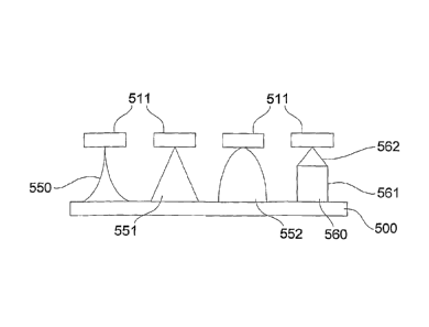
Figures 5A to 5C are schematic diagrams of an example of the steps in etching
projections in
a substrate;
Figures 6A to 6C are examples of secondary electron images of projections
produced using
different etching times;
Figure 7 is a graph illustrating an example of the effect of mask dots size
and array pitch on
etch depth;
Figures 8A to 8C are graphs illustrating examples of the variation in vertical
etch rates
depending on C4F8:SF6 ratios, gas flow rates and gas pressures respectively;
Figure 9 is a graph illustrating an example of the effect of gas flow rates on
projection tip
angle;
Figure 10 is a graph illustrating an example of the effect of system pressure
on lateral etch
rates;
Figure 11 is a graph illustrating an example of the effect of system pressure
on etch
uniformity;
Figure 12 is a graph illustrating an example of the effect of C4F8:SF6 ratio
on projection
length;
Figures 13A to 13C are examples of secondary electron images of projections
following an
02 plasma clean; an ultrasonic bath clean; and oxidation and HF sharpening,
respectively;
Figures 14A to 14C are secondary electron images of example patches including
projections
having lengths of 60, 100 and 150 pm, respectively; and,
Figure 14D is a secondary electron image of a projection patch after insertion
into a subject;
Figures 15A and 15B are examples of secondary electron images of projections
obtained
using a high rate Oerlikon etching system;
Figures 16A and 16B are examples of secondary electron images of projections
obtained
using a high rate STS etching system;
CA 02749347 2011-07-11
WO 2009/097660
PCT/AU2009/000142
- 9 -
Figure 17 is an example of a secondary electron images of projections obtained
using a lower
system pressure and power; Figures 18A to 18E are secondary electron images of
examples
of projections having a conical straight edge profile;
Figures 19A and 19B are secondary electron images of examples of projections
having a
conical convex edge profile;
Figures 20A to 20E are secondary electron images of examples of projections
having a
stepped profile;
Figure 21 is a secondary electron image of examples of projections having a
hyper sharp tip;
Figure 22 is a secondary electron image of examples of projections having a
conical convex
edge generated using a ramped etch process;
Figures 23A and 23B are secondary electron images of examples of projection
arrays having
coated and uncoated projections respectively;
Figures 24A and 24B are examples of CryoSEM images illustrating the
penetration of skin
by the projections on a patch;
Figures 25A and 25B are examples of CryoSEM images illustrating the
penetration of skin
by the projections on a patch;
Figures 26A and 26B are secondary electron images of a patch after application
to mouse ear
skin.
Detailed Description of the Preferred Embodiments
An example of a device for delivering material to targets within a body will
now be described
with reference to Figures lA to IF.
In this example, the device is in the form of patch 100 having a number of
projections 110
provided on a surface 121 of a substrate 120. The projections 110 and
substrate 120 may be
formed from any suitable material, but in one example, are formed from a
silicon type
material. The projections may be solid, non-porous and non-hollow, although
this is not
essential.
In the example shown, the patch has a width W and a breadth B vvith the
projections 110
being separated by spacing S.
CA 02749347 2011-07-11
WO 2009/097660 PCT/AU2009/000142
- 10 -
In use, the patch 100 is positioned against a surface of a subject, allowing
the projections to
enter the surface and provide material to targets therein. An example of this
is shown in
Figure 1C.
In this example, the patch 100 is urged against a subject's skin shown
generally at 150, so that
the projections 110 pierce the Stratum Corneum 160, and enter the Viable
Epidermis 170 to
reach targets of interest, shown generally at 180. However, this is not
essential and the patch
can be used to deliver material to any part or region in the subject.
It will be appreciated that the projections can have a variety of shapes, and
examples of
suitable projection shapes are shown in more detail in Figures 1D, 1E and 1F.
In one example, the projection includes a targeting section 111, intended to
deliver the
material or stimulus to targets within the body, and a support section 112 for
supporting the
targeting section 111. However, this is not essential, and a single element
may be used.
In the example of Figure 1D, the projection is formed from a conically shaped
member,
which tapers gradually along its entire length. In this example, the targeting
section 111 is
therefore defined to be the part of the projection having a diameter of less
than dz.
In Figures lE and 1F, the structure of the projection may vary along its
length to provide a
defined targeting section 111 with a designed structure. In the example of
Figure 1E, the
targeting section 111 is in the form of a substantially cylindrical shape,
such that the diameter
dr is approximately equal to the diameter d2, with a tapered support section,
such that the
diameter d2 is smaller than the diameter d3. In contrast, in the example of
Figure 1F, the
targeting section 111 is in the form of taper such that the diameter dr is
smaller than the
diameter d2, with a cylindrical support section, such that the diameter d2 is
substantially equal
to the diameter d3.
In general, the support section 112 has a length a, whilst the targeting
section 111 has a
length l. The diameter of the tip is indicated by dr, whilst the diameter of
the support section
base is given by d3.
CA 02749347 2015-10-22
- 11 -
In use, the device can be used to deliver material to specific targets within
the body or more
generally to the blood supply, or tissue within the body and the configuration
of the device
will tend to depend on its intended use.
Thus, for example, if the patch is configured so as to ensure material is
delivered to specific
targets such as cells, then it may be necessary to select a more specific
arrangement of
projections than if delivery is provided more generally to the blood. To
achieve this, the
device can be provided with a particular configuration of patch parameters to
ensure specific
targeting. The patch parameters can include the number of projections N, the
spacing S
between projections, and the projection size and shape. This is described in
more detail in
co-pending US Publication No. 2011/0245776.
In one specific example, a patch having a surface area of approximately 0.16
cm2 has
projections provided at a density of between 1,000-30,000 projections/cm2, and
typically at a
density of approximately 20,000 projections/cm2. However, alternative
dimensions can be
used. For example, a patch for an animal such as a mouse may have a surface
area of 0.32 to
0.48 cm2, whereas as a patch for a human may have a surface area of
approximately 1 cm2.
variety of surface areas can be achieved by mounting a suitable number and
arrangement of
patches on a common substrate.
The projections typically have a length of between 10 to 200 vim and typically
90 vim with a
radius of curvature of greater than 1 vim and more typically greater than 5
vim. However, it
will be appreciated that other dimensions may be used.
If distinct targeting section and support sections are provided, the targeting
section typically
has a diameter of less than 1 um and more typically less than 0.5 vim. The
length of the
targeting section is typically less than 100 vim, less than 10 pm and
typically less than 5 vim.
The length of the support section typically varies depending on the location
of the target
within the subject. Example lengths include less than 200 pm for epidermal
delivery, less
than 1000 vim for dermal cell delivery, 600-800 vim for delivery to basal
cells in the
epithelium of the mucosa and approximately 100 vim for lung delivery.
A process for the production of projections on a patch will now be described.
CA 02749347 2011-07-11
WO 2009/097660
PCT/AU2009/000142
- 12 -
In one example, the process includes providing a mask on a substrate and
etching the
substrate using an etchant and a passivant to thereby control the etching
process and form the
proj ections.
The etchant is typically a compound formed from a group 16 element and a
halide. In one
example, the etchant contains sulphur and fluorine, and may therefore include
sulphur hex-
fluoride (SF6) or the like.
The passivant is typically a gas other than oxygen, and in particular
typically includes a
group 14 element and a halide. In one example, the passivant is a per-fluoride
hydrocarbon
such as octafluorocyclobutane (C4F8).
The use of suitable etchants and passivants other than oxygen allows for a
high degree of
control to be provided over the etching process. In particular, adjusting etch
parameters such
as the passivant to etchant ratio, the gas flow and the system pressure, this
allows etching
rates to be controlled. This in turn allows the degree to which the process is
isotropic or
anisoptropic to be adjusted. By controlling the relative characteristics, this
allows the shape
of the resulting projections to be carefully controlled.
The mask may be provided on the substrate using any one of a suitable number
of techniques.
However, in one example, this is achieved by applying a mask material to the
substrate and
then selectively exposing the mask material to radiation to thereby form the
mask. When
passivants other than oxygen are used, the mask material can be formed from an
organic
1 photo-resist, such as a crosslinked epoxy resin based polymer. An example
of such a material
is Su-8 2000 supplied by MicroChem Corp, although other similar related
materials can be
used. Polymer masks are generally significantly easier to create and use,
resulting in the
process being significantly cheaper than when a hard mask, such as a metal
mask is used.
Accordingly, the above described technique allows for the production of
silicon projections
to be completed using a combination of optical lithography and deep silicon
etching. This
allows the profile of the projections to be carefully controlled, thereby
allowing projections
suitable for use in a range of applications to be created.
CA 02749347 2011-07-11
WO 2009/097660
PCT/AU2009/000142
- 13 -
Prior art techniques utilising fluorine/oxygen chemistry provide only
extremely limited
control over the etching process. This is in part due to the formation of a
SiliconOxyFluoride
layer on the surface of the wafer as part of the passivation process.
Formation of the layer
occurs rapidly and is difficult to control. Furthermore, the hardness of the
layer means that it
tends to interfere with the remainder of the etch process. As a result, it is
generally only
possible to produce projections having a concaved profile, which in turn
results in a narrow
tip that is thin and liable to breakage. A secondary electron image of an
example of a
concave profiled projection is shown in Figure 2.
In contrast to this, by using a suitable alternative passivant to thereby
control the etching
process, this avoids the formation of a SiliconOxyFluoride layer, which in
turn allows a
greater control over projection shape to be achieved. In one example, this can
be used to
allow for a more straight profiled conical shape to be produced, an example of
which is
shown in Figure 3. By virtue of the thicker tip shape, this provides for more
robust
projections which are more capable of delivery of material or stimulus to a
desired target
within a subject. Other shapes can also be provided for, as will be described
in more detail
below.
Further benefits are also obtained. In particular, the use of the above
described passivants
and etchants, allows an organic based photo-resists to be used as masks,
instead of the metal
required by the prior art. The organic based photo-resist masks are easier and
cheaper to
produce. Additionally, these can be of a reduced height as compared to the
metal masks
required in fluorine/oxygen based etching processes, which in turn provides
further control
over the resulting patch geometry.
In addition to the steps described above, following formation of the
projections, one or more
post-etch processing steps may be performed.
In one example, following formation of the projections, the projections
undergo a chemical
sharpening process. Chemical sharpening is performed so as to reduce the
roughness of the
projections, which can in turn enhance the ability of the projections to
deliver material or
stimulus to targets within the subject. Sharpening may be achieved in any one
of a number of
manners, but in one example, is achieved by forming a silicon dioxide layer on
the
CA 02749347 2011-07-11
WO 2009/097660
PCT/AU2009/000142
- 14 -
projections and then subsequently removing the silicon dioxide layer. This
process will be
described in more detail below.
A further post-etch process that may be performed is to coat the projections.
Any suitable
coating may be used, and this can include coating the projections with a
material to be
delivered to the subject, as described for example in co-pending application
AU-
2007907092. Additionally, and/or alternatively, the projection may be coated
with a metallic
material such as gold. This can assist binding of other material to the
projection, and can also
improve surface properties to assist in material delivery to the subject. An
example of a gold
coated projection is shown in Figure 4.
Examples of the process will now be described in more detail with reference to
Figures 5A to
5C.
In this example, the first step is to produce a plasma etch mask. To achieve
this, a suitable
mask material, such as Su-8, which is a photoreactive polymer, is applied to a
substrate 500,
which in one example is 4 inch, 500 gm thick 100 silicon wafer. The substrate
500 is then
spun at an appropriate speed to distribute polymer in a layer 510 over a
surface 501 of the
substrate 500. The spin speed is selected to control the thickness of the mask
layer 510. In
one example, to form a projection having a length in the region of 50-70 i.tm,
the mask layer
510 has a thickness in the region of 7-8 um. It will be appreciated that a
thicker mask, such
as up to 30 gm may be used.
The substrate 500 and mask layer 510 are optionally treated. This may be
performed, for
example to remove any excess solvent, which can be achieved by soft baking the
substrate
500 and layer 510 for five minutes at 95 C.
Once suitably prepared, the mask layer 510 can be selectively exposed with
radiation 520 to
cause the exposed mask material to harden. In one example, this is achieved
using a suitable
photo-mask 530 and radiation source. Thus, exposure of the Su-8 film can be
performed
using chromium on quartz photo-mask and a Carl Suss MA6 mask aligner set to
supply
10mJ/second UV light. Typically complete cross-linking of the Su-8 polymer
occurs after
1.8 seconds of exposure for 1 gm of Su-8 thickness, although longer exposure
of up to 30
seconds can be used to ensure complete cross-linking of mask layers.
CA 02749347 2011-07-11
WO 2009/097660
PCT/AU2009/000142
- 15 -
The substrate 500 and mask layer 510 may again be optionally treated, for
example by baking
for one minute at 95 C. This can be used to promote the formation and release
of a Lewis
Acids which aids the cross-linking process and formation of a straight
sidewall profile for the
mask.
The unexposed mask material can be removed using a suitable solvent. Thus, in
the above,
the uncross-linked Su-8 can be removed by developing in EC solvent (PGMEA) for
two
minutes. The complete removal of uncross-linked Su-8 can be confirmed by
washing the
wafer with IPA. If a white precipitated is observed (indicating uncompleted
development)
the wafer is replaced in the EC solvent for further 30 seconds. Development is
completed
until no white precipitated is observed upon washing with IPA. The excess IPA
can be
removed by blow drying with dry nitrogen gas.
Further treatment may then be performed, such as hard baking of the wafer 500
at 100 C for
five minutes. This can be used to harden and remove residual developer and IPA
for the Su-8
mask. At this stage in the process, the mask layer 510 includes a number of
dots 511, as
shown in Figure 5B. The next stage in the process is the formation of
projections by etching.
In one example, this is achieved using plasma etching, which can be completed
on an STS
(Surface Technology Systems) ASE (Advanced Silicon Etch) system. In one
example, this is
achieved using SF6 as the etch gas and C4F8 as the passivation gas, although
as described
above, other gases can be used.
Controlled continuous isotropic plasma etch process was complete with a plasma
gas mixture
of SF6:C4F8 typically in the ratio range of 0.25 to 0.60. Vertical, horizontal
and projection tip
angle can be controlled to provide required projection profiles. This is
achieved by ramping
or varying the plasma gas condition throughout the etch process, by changing
the rate of gas
flow, pressure and SF6: C4F8 ratios.
; In one example, by performing a continuous etch for approximately 30-60
minutes,
projection profiles of concave to convex shapes can be achieved, as shown at
550, 551, 552
in Figure 5C. Example projection profiles obtained in performing etching under
similar
conditions, but for different time periods are shown in Figures 6A to 6C,
which show the
result of etching for 40 mins, 45 mins and 50 mins respectively. In this
instance, the images
CA 02749347 2011-07-11
WO 2009/097660 PCT/AU2009/000142
- 16 -
highlight how the longer etching time results in a narrower taller projection,
as would be
expected by the increased amount of etching.
A further alternative, etching can be performed in multiple stages to provide
additional
control. In one example, a continuous etch is performed for approximately 30-
60 minutes,
with a subsequent etch being performed for a further 15-30 minutes. This
allows a projection
560 having a column shaped supporting section 561 and a conical tip 562 to be
produced, as
shown in Figure 5C.
In one example, the profile of the projection can be formed by altering
etching parameters,
such as the SF6:C4F8 ratio, pressures, or the like, between the different etch
steps.
Additionally, the wafer 500 can be removed from the ASE system, allowing the
wafer and/or
passivant to react with the ambient atmosphere. This can alter the effect of
the passivant,
thereby altering the profiles that can be produced.
The ability to pause the etching process allows further control over the
etching process. For
example, the etching can be performed to near completion, with the process
then being halted
to allow the wafer or patches to be examined to determine the amount of
etching required to
complete the process. The process can then be resumed and completed.
Pausing the etching process can be performed as the passivant binds only
relatively weakly to
the silicon surface. Consequently, even when the passivant has reacted with
the ambient air
outside the etching system, the passivant can still be removed when etching
recommences. In
contrast, in fluorine/oxygen based etching techniques, the passivant binds
strongly to the
silicon surface through covalent bonding. Consequently, when the wafer is
removed from
the etching system an oxide layer is formed which cannot be controllably
etched. This
prevents fluorine/oxygen based etching process from being halted or paused to
allow
examination of the wafer, which in turn limits the degree of control that can
be achieved.
This effect is particularly exacerbated when etching narrow projections, as
the etching has a
faster effect as the projection narrows, and the etch nears completion. As a
result, when
etching narrow projections using a fluorine/oxygen based etching approach,
over etching
CA 02749347 2011-07-11
WO 2009/097660 PCT/AU2009/000142
- 17 -
often occurs, resulting in projections that are too narrow and hence fragile
to use. This
renders the resulting patches useless, which in turn leads to increased
manufacturing costs."
The achievable height of the projections is dependent on a number of factors,
such as the size
and pitch (separation) of mask dots. An example of the effect of mask dots
size and array
pitch on etch depth is shown in Figure 7. To form projections having a height
in the region
of 70 m, the dots are typically formed with a diameter in the region of 7-8
gm. This is a
smaller dot size than is typically required in a fluorine/oxygen based plasma
etching
technique.
Additionally, plasma conditions effect projection profile control such that
vertical silicon etch
rates decrease with increasing C4F8:SF6 ratios, lower gas flow rates and low
gas pressures as
shown in Figures 8A to 8C.
Similarly lateral etch rates are effected, such that by increasing C4F8:SF6
ratios results in a
more anisotropic etch. By increasing total gas flow or system pressure an
increased isotropic
etch is observed, producing a more concave shaped of projection. The effect of
gas flow
rates on tip angle is shown in Figure 9, with the effect of over pressure on
lateral etch rates
being shown in Figure 10. Figure 11 is a graph illustrating an example of the
effect of
system pressure on etch uniformity. This illustrates that in general a lower
pressure of below
1.3 Pa (10 mT) is preferred to ensure good etch uniformity.
Figure 12 is a graph of the effect of C4F8:SF6 ratio on projection length for
etching performed
using a 50 [tm dot 70 i.tm pitch mask, at 0.3 Pa (2.5 mT), total flow rate 100
sccm and power
800 watts. This illustrates that as the C4F8:SF6 ratio increases, so does the
projection length
that can be achieved.
Typically etchant is supplied at a flow rate in the range of 0 to 200 sccm
(standard centimetre
cube per minute), and more typically in the range of 40 to 120 sccm. Passivant
may be
supplied at a flow rate in the range of 0 to 200 sccm, and more typically in
the range of 10 to
80 sccm.
Accordingly, by varying etch parameters such as the passivant to etchant
ratio, the gas flow
and the system pressure, this allows projection heights and profiles to be
well defined.
CA 02749347 2011-07-11
WO 2009/097660 PCT/AU2009/000142
- 18 -
Additionally, by appropriate selection of etch parameters, the bullseye effect
can be
dramatically reduced when compared to fluorine/oxygen etches, thereby
increasing the
amount of useable patches that can be obtained from a etching process, which
in turn
increases the cost effectiveness of the process.
In one example, to obtain greater projection lengths, a conventional switched
BORSH
process can be performed. However, this is not essential and may depend on the
system being
used to perform the etching process.
Following completion of the etching, the etch mask can be removed and the
silicon wafer
chemical cleaned. This can be performed using an oxygen plasma and washing of
silicon
wafer in micro-strip (concentrated H2SO4 peroxide mixture).
Sharpening of the projections can be achieved via the formation of a silicon
dioxide layer on
the projections by heating the projections in an oxygen rich environment. In
one example, a
1-2 tm thick layer of thermal silicon dioxide is formed by heating at 1050 C
under oxygen
for 24-48 hours. The oxide is subsequently removed using 10% HF and washing in
distilled
water.
Examples of the appearance of the projections after cleaning with 02 plasma,
after an
ultrasonic bath clean and following oxidation and HF sharpening are shown in
Figures 13A
to 13C. These highlight how the cleaning and sharpening process result in
smooth
projections that are ideal for skin penetration.
Further optional treatment can be performed such as baking the wafer at 100 C
for 10
minutes to remove residual water.
Following this, gold coating can optionally be preformed using a DC sputter
coating system.
To achieve this, it is typical to clean the wafer surface using Argon gas
sputtering before the
depositing 50 run of Chromium to act as an adhesion layer, followed by 100 nm
of Gold.
A further benefit of the provision of a gold coating is to enhance the
physical properties of
the projections. Silicon tends to be brittle and as a result can fracture in
use due to crack
growth. However, the gold provide a soft ductile coating, which tends to
absorb unwanted
CA 02749347 2011-07-11
WO 2009/097660
PCT/AU2009/000142
- 19 -
forces and impacts, thereby enhancing the resilience of the projections and
reducing their
failure rate in use.
The final wafer may be further cleaned using Argon gas sputtering.
Examples of patches including 60, 100 and 150 pm length projections are shown
in Figures
14A to 14C. An example of a projection patch after insertion into a subject is
shown in
Figure 14D. It can be seen that the projections remain unbroken, highlighting
that the
projections are strong enough to remain intact after insertion into the
subject.
The use of the processes described above can provide any one or more of a
number of
advantages.
For example, the use of a suitable passivation gas such as C4F8 allows the
direct use of an
organic photo-resist (for example Su-8). Su-8 is a high aspect ratio negative
resist with good
plasma etching properties (i.e. selectivity). A greatly increased selectivity
of mask to silicon
etching is found when using a passivant other than oxygen, such as C4F8. This
allows for a
simplification in manufacturing by reducing the number of process steps.
Firstly the need for
deposition of a hard etch mask is removed (no deposition of metals or
dielectric required),
secondly etching of the hard mask not required and thirdly removal photo-
resist not
necessary.
Su-8 is suitable for use in both anisotropic and isotropic etching. Using Su-8
as an etch mask
provides a considerable reducing in production costs and time compared to
prior art
processes.
Using a passivation gas such as C4F8 allows a greater control over projection
tip profiles to be
provided. The use of oxygen as a passivation, gas unless employed in a cryo
ICP system,
will produce a concave profile. However, cryo ICP systems are generally
expensive to
operate and maintain, thereby making this technique unsuitable for use on a
mass scale.
Using C4F8 as a passivation gas, projections with profiles of concave, flat
and convex form
can be produced. The use of parameter ramping allows a high degree of tip
profile control to
be maintained.
CA 02749347 2011-07-11
WO 2009/097660
PCT/AU2009/000142
- 20 -
Additionally, etching can be paused, allowing additional control over the
etching process.
This can be used to allow a range of different projection profiles to be
produced, as well as to
control termination of the etching process more accurately.
The use of fluorocarbons, such as C4F8 also reduces the impact of the bullseye
effect, thereby
increasing the amount of useable patches resulting from the etching process.
Chemical sharpening and surface morphology changes to silicon projection tips.
Chemical
sharpening to <10 nm tip diameter can be achieved, allowing for easier
penetration of the
stratum comeum with less pressure being required.
Wet and dry oxidation sharpening methods can be used. Morphological
differences have
been observed between wet and dry oxidation conditions consequently smooth or
porous
surface structure can be produced respectively. Porosity can also be further
increased using
electrochemical methods.
Gold can be used as an adhesion layer for delivery of DNA and biological
materials with
using the projections. This can also enhance the physical properties of the
projections,
thereby reducing their failure rate.
Accordingly, the above described process provides for the more efficient and
cost effective
manufacture of projections by plasma etching, as well as enabling greater
control over the
etching process, to allow specific projection profiles to be created.
A number of example projection shapes are shown in Figures 15A, 15B, 16A, and
16B.
In the examples of Figures 15A and 15B, etching is performed as a two step
process, using a
SF6:C4F8 ratio 2.5 for the first step and a SF6:C4F8 ratio 1.2 for the second
step. Both steps
are performed at 2000 watts, 200 sccm total gas flow and 26.6 Pa (200 mT)
pressure, using
an Oerlikon etching system, which typically can etch at higher rates that the
STS ASE system
discussed above. In these examples a grainy structure is present at the top of
the projections
; due to excess HF in the chamber.
Figures 16A and 16B show similar results are obtained for a high rate STS
etch. In this
example, the projections have a length of 120 gin. The creation of a grainy
structure can be
CA 02749347 2011-07-11
WO 2009/097660
PCT/AU2009/000142
-21 -
reduced either by using a lower system power and pressure, which results in
the smooth
shaped projections shown in Figure 17. However, in this example, the reduced
pressure and
power results in a shorter projection having a length of 80 pm, for similar
etching parameters.
Example patch configuration produced using the above described etching
techniques will
now be described with reference to Figures 18 to 22.
In the example of Figures 18A and 18E, a single stage etching process is used
to produce
projections having a conical shape.
For the example of Figures 18A and 18B, the etching parameters are broadly as
set out
below, resulting in projections having a length of approximately 50-70 [tm
depth, sub-micron
sharp, 3-to-1 base to length aspect ratio, with a straight edge profile:
Etch mask 30 1.tm dot with 70 gm pitch;
Resist: Su8-5 spun to give 10 Jim thickness
Etch: 36 sccm C4F8 passivant, 64sccm SF6etchant,
pressure 0.3 Pa (2.5 mT),
power 800 watts coil, 20 watts platen
time 50 minutes.
A similar single stage etching process can be used with different etching
parameters to
produce projections have dimensions of 30 gm length, 70 pm spacing; 50 pm
length, 70 pm
spacing; and 70 pm length, 100 gm spacing, as shown in Figures 18C to 18E,
respectively. It
will be appreciated from this that a range of different conical projections
can be produced and
that these are for the purpose of example only.
In the example of Figures 19A and 19B, a single stage etching process is used
to produce
projections having a conical shape, with a convex profile edge. In this
example, using the
etching parameters set out below, the projections typically have a length of
approximately
150 pm, sub-micron sharp, 5-to-1 base to length aspect ratio, with a convex
profile:
Etch mask 50 m dot with 70 pm pitch
Resist: Su8-25 spun to give 25 p.m thickness
Etch: gases 37s ccm C4F8passivant, 63 sccm SF6etchant,
pressure 0.3 Pa (2.5 mT),
CA 02749347 2011-07-11
WO 2009/097660
PCT/AU2009/000142
- 22 -
power 800 watts coil, 20 watts platen
time 2 hours 15 minutes
In the examples of Figures 20A to 20E, a two stage etching process is used to
produce
stepped projections having a cylindrical base and conical shaped tip.
For the example of Figures 20A and 20B, the etching parameters are broadly as
set out
below, resulting in projections having a length of approximately 150 gm depth,
hyper sharp,
5-to-1 base to length aspect ratio:
Etch mask 30 gm dot with 70 gm pitch
Resist: Su8-5 spun to give 10 gm thickness
Etch: gases 36 sccm C4F8 passivant, 64 sccm SF6etchant,
pressure 0.3 Pa (2.5 mT),
power 800 watts coil, 20 watts platen
time 50 minutes
1 hour conventional ASE switched etch
In the examples of Figures 20C to 20E, alternative parameters are used to
produce
projections having lengths of 80 gm, 110 gm, and 65 gm respectively.
For the example of Figure 21, the etching parameters are broadly as set out
below, resulting
in projections having a length of approximately 80-90 gm depth, hyper sharp, 5-
to-1 base to
length aspect ratio:
Etch mask 30 gm dot with 70 gm pitch
Resist: Su8-5 spun to give 15 gm thickness
Etch: gases 38 sccm C4F8 passivant, 62 sccm SF6 etchant,
pressure 0.3 Pa (2.5 mT),
power 800 watts coil, 20 watts platen
time 90 minutes
For the example of Figure 22, the etching parameters are broadly as set out
below. In this
instance, a ramped etch is performed to result in a convex edge profile on
projections having
a length of approximately 60-70 gm:
Etch mask 30 gm dot with 70 gm pitch
CA 02749347 2011-07-11
WO 2009/097660
PCT/AU2009/000142
- 23 -
Resist: Su8-5 spun to give 15 gm thickness
Etch: gases 50-80 sccm C4F8 passivant, 120 sccm SF6etchant,
pressure 0.3 Pa (2.5 mT),
power 800 watts coil, 20 watts platen
time 60 minutes - C4F8 gas ramped 0.5 sccm per minute
It will be appreciated that the example etching parameters described above are
for the
purpose of example only and are not intended to be limiting. For example, the
parameters
will typically be etching system specific, so that if similar dimensioned
projections are to be
produced using different etching equipment, appropriate modification of the
parameters will
be required.
Example experiments used to demonstrate the effectiveness of the projections
at delivering
material to subjects will now be described.
The tissue used in this experiment was mouse ear skin from 7 week old C57
Black6 female
mice. Experimentation was performed in-vivo following injection of Ketamil-
Xylasil
anaesthetic (Troy laboratories Pty., Ltd., Smithfield, Australia), in
accordance with
Australian Animal Ethics guidelines. In-vivo tests ensured that blood flow was
maintained to
the skin to highlight erythema and blood vessel damage resulting from
application. Five ears
(n=5) were used per group in dye delivery and Cryo-SEM experiments.
The projection patches used for this study were designed to give a high
probability of
Langerhans cell-antigen interaction. The patches are fabricated using the
etching techniques
outlined above in a two step process, to thereby produce projections having a
stepped
configuration including a conical tip and cylindrical base. In this example,
the projections
have a length of 65 gm and a 50 gm conical section, atop a 15 gm cylindrical
base. The
projections have a density of 20,000/cm2, with 4mm x 4mm projection area on a
5mm x 5mm
silicon base.
The delivery system for this experiment is a solid coating on the surface of
the projections.
This coating dissolves once wetted in the skin for the vaccine delivery. These
studies were
designed to emulate vaccine delivery. 84, solution of 0.4% Vybrant DiD (a
lipophilic
fluorescent dye, Molecular Probes Inc., Eugene, Oregon) and 1.5%
Methylcellulose was
CA 02749347 2011-07-11
WO 2009/097660
PCT/AU2009/000142
- 24 -
coated on the array using a nitrogen jet method described in copending
application number
PCT/A112008/001903. The dye is used to provide projection penetration tracks
when the dye
is released from the projections. Concentrations in solution were titrated for
minimal
diffusion following insertion.
Examples of coated and uncoated patches are shown in Figures 23A and 23B.
After patch application, the skin is prepared for confocal section dye
measurement. To do
this the skin is fixed in 2% Paraformaldehyde in 0.1 M Phosphate buffer,
preceding cryo-
preservation. Once frozen, 10 um thick sections of skin were cut on a cryostat
before
imaging on a Zeiss LSM510 Meta confocal Multi-Photon Microscope (Carl Zeiss,
Inc.,
Germany). Dye delivery highlighting projection tracks were measured in length
from the
point where the stratum corneum was breached at the edge of the hole, to the
lowest dye
point in the skin. An example of the sections used are shown in Figure 24A and
24B.
Projection holes with significant stratum corneum deflection, obscuring the
viable epidermis,
were neglected as they represent incomplete penetration.
Surface data from microscopy allows information regarding projection
penetration to be
determined. This was done using a Scanning Electron Microscope (SEM) fitted
with a cryo-
stage and preparation chamber (Oxford CT-1500 and Philips XL30 SEM, Philips,
Netherlands). For these studies the patches were coated as before, before
application to the
skin. The patch was applied to the skin in the same manner as in the dye
studies. The patch
and skin assembly was then slush frozen in liquid nitrogen (LN2) and
transferred to a cryo-
preservation chamber under vacuum. At this point the patch was removed from
the skin and
the skin then sputter coated with a thin (few nanometres) layer of gold for
imaging purposes.
This technique ensures that the holes in the surface of the skin are as they
would be in-situ.
Skin morphology changes are restricted by the projections during the freezing,
allowing
accurate quantification. Imaging is then performed by SEM.
Application of an MNP patch to skin results in penetrative channels through
the stratum
corneum to lower layers of the skin, as shown in Figures 25A and 25B, in which
significant
holes are created over almost the complete 4mm x 4mm area of the patch.
CA 02749347 2011-07-11
WO 2009/097660
PCT/AU2009/000142
- 25 -
Using this technique the surface profile is clear, with individual corneocytes
distinguishable.
The location of the micro-channels with respect to the corneocytes (between or
through) was
seen to have no effect on penetration. The surface data also shows that areas
with hair are
punctured similarly to those without, indicating that the projections are not
affected by hairs,
simply puncturing through or adjacent to them.
The Cryo-SEM data also allows examination of the patch post-application where
it is
removed and an upper layer of corneocytes has remained on the projections.
Figure 26A
shows the entire patch after application to mouse ear skin, whilst Figure 268
shows a close-
up of nine projections. The images show that the patch has large areas covered
by
corneocytes which have been frozen with liquid nitrogen showing their
profiles. The frozen
corneocytes reveal penetration profiles and show the bulk behaviour of the
outermost layer of
skin. It is clear that for the case shown, the step in conical projection
geometry is acting to
restrain entrance to the skin. This is also evident in the Figure 18C where
there are circular
impressions around projection holes at higher velocities indicative of the
step reaching the
skin. Projection progression appears to have been restricted by this.
The quantitative measurement of penetration performance of our MNP patch is
from raw data
such as the typical histological section shown in Figures 24A and 24B. This
shows a section
of mouse ear skin and the corresponding dye delivered. This can be used to
measure delivery
depth of dye payload, showing successful delivery beyond the stratum comeum.
These data
show that this device is capable of delivering molecules into the skin.
It is noticeable that the greatest penetration for these projections is
approximately 65% of
their conical length, which corresponds to the location at which skin reaches
the step in
geometry. In particular, when the cylindrical portion of the projections reach
the surface of
the skin they present a larger cross-sectional area to the corneocytes that
they are touching,
allowing the patch to be decelerated and penetration stopped. This is
highlighted by viewing
the treated area of skin after a 1.96 m/s application, where clear circular
impressions around
the projection holes are visible as shown in Figure 25B.
Accordingly, it will be appreciated that the ability to perform a two step
etch, and hence
produce a stepped projection profile, allows the depth of projection
penetration to be
CA 02749347 2011-07-11
WO 2009/097660
PCT/AU2009/000142
- 26 -
controlled in use, which can in turn be used to deliver payloads to specific
cells or layers of
cells in the skin. For example, in the case of vaccines, the viable epidermis,
and Langerhans
cells therein can be targeted directly using a stepped projection profile of
appropriate length.
A number of further variations and options for use with the above described
devices will now
be described.
Herein, the terms "projection", "micro-nanoprojection", "nanoneedle",
"nanoprojection",
"needle", "rod" etc are used interchangeably to describe the projections.
The projections may be used for delivery not only through the skin but through
other body
surfaces, including mucosa' surfaces, to cellular sites below the outer layer
or layers of such
surfaces.
The device is suitable for intracellular delivery. The device is suitable for
delivery to specific
organelles within cells. Examples of organelles to which the device can be
applied include a
cell nucleus, or endoplasmic reticulum, for example.
In one example the device is provided having a needle support section, that is
to say the
projections comprise a suitable support section, of sufficient length to reach
the desired site
and a (needle) delivery end section having a length no greater than 20 microns
and a
maximum width no greater than 5 microns, preferably no greater than 2 microns.
In one example, the maximum width of the delivery end section is no greater
than 1000 nm,
even more preferably the maximum width of the delivery end section is no
greater than 500
nm.
In a further example, the device is for mucosal delivery. This device may have
a needle
support section, that is to say the projections comprise a suitable support
section, of sufficient
length to reach the desired site, such as of length at least 100 microns and a
(needle) delivery
end section having a length no greater than 20 microns and a maximum width no
greater than
microns, preferably no greater than 2 microns.
CA 02749347 2011-07-11
WO 2009/097660
PCT/AU2009/000142
- 27 -
In one example, the device of the invention is for delivery to lung, eye,
cornea, sclera or other
internal organ or tissue. In a further example, the device is for in-vitro
delivery to tissue, cell
cultures, cell lines, organs, artificial tissues and tissue engineered
products. This device
typically has a needle support section, that is to say the projections
comprise a suitable
support section, of length at least 5 microns and a needle delivery end
section having a length
no greater than 20 microns and a maximum width no greater than 5 microns,
preferably no
greater than 2 microns.
In one example, the device comprises projections in which the (needle)
delivery end section
and support length, that is to say the "needle support section", is coated
with a bioactive
material across the whole or part of its length, as described in further
detail in the copending
application AU- 2007907092. The (needle) delivery end section and support
length may be
coated on selective areas thereof. This may depend upon the bioactive material
being used or
the target selected for example.
In a further example, a bioactive material is releasably incorporated into the
material of
which the needle, or projection, is composed. All, or part of the projection
may be
constructed of a biocompatible, biodegradable polymer (such as Poly Lactic
Acid (PLA),
PolyGlycolic Acid (PGA) or PGLA or Poly Glucleic Acid), which is formulated
with the
bioactive material of choice. The projections may then be inserted into the
appropriate target
site and, as they dissolve, the bioactive material will enter the
organelle(s)/cells.
In one aspect, the device is provided in the form of a patch containing a
plurality of needles
(projections) for application to a body surface. A multiplicity of projections
can allow
multiple cells and organelles to be targeted and provided with a material at
the same time.
The patch may be of any suitable shape, such as square or round for example.
The overall
number of projections per patch depends upon the particular application in
which the device
; is to be used. Preferably, the patch has at least 10 needles per mm, and
more preferably at
least 100 needles per mm2. Considerations and specific examples of such a
patch are
provided in more detail below.
As an alternative to a gold coating, any suitable biocompatible material may
be provided as a
coating, such as Titanium, Silver, Silicon, or the like. This may be the
entire device, or
CA 02749347 2015-10-22
- 28 -
alternatively it may only be the projections or the delivery end section of
the projections
which are made from the biocompatible materials.
An alternative means for producing masks is with 2 photon Stereolithography, a
technique
which is known in the art and is described in more detail below.
The device may be for a single use or may be used and then recoated with the
same or a
different bioactive material or other stimulus, for example.
In one example, the device comprises projections which are of differing
lengths and/or
diameters (or thicknesses depending on the shape of the projections) to allow
targeting of
different targets within the same use of the device.
Thus, a number of preferred embodiments have been fully described above with
reference to
the drawing figures. The scope of the claims should not be limited by the
preferred
embodiments and examples, but should be given the broadest interpretation
consistent with
the description as a whole.