Note: Descriptions are shown in the official language in which they were submitted.
CA 02749423 2011-08-15
CONNECTOR FOR PV CELLS AND METHOD FOR ITS PRODUCTION
Description
The invention relates to a connector for PV cells (photovoltaic cells or
wafers; In the
following "PV cell" will be meant to include õPV wafer".) comprising a strip
of electrically
conductive material which has a flat cross-section with a first and a second
broad side
extending over its entire length and with two narrow sides which each connect
opposite
edges of the broad sides, wherein at least the first broad side has a
corrugated structure
running in longitudinal direction of the strip. The invention also relates to
a method for
producing such connectors for PV cells.
Connectors for PV cells are usually supplied wound as long ribbons on rolls
and are then
cut off individually from these ribbons. The definition of the first and
second broad side or
the top and bottom is governed by the winding in the finished supplied form
and can to this
extent be as desired. In the present description, the first broad side or top
is designated
the side facing the incoming sunlight (so-called "sunny side").
Connectors are used in photovoltaics in order to connect the individual PV
cells to a PV
module. Five PV cells for example are series-connected by means of the
connectors.
Each connector creates the electrical connection between two consecutive cells
of a PV
module. As a rule the connectors are used with PV cells of crystallized
silicon. However,
they can also be used in thin-film PV cells. The connectors are to securely
join together
the electric poles (positive and negative) of adjacent cells within the PV
module,
corresponding to the desired connection. As the PV cells are connected in
series (positive
to negative) and the orientation of the poles of each cell is the same, the
connector is
soldered to the top (so-called "sunny side") of one cell and then to the
bottom (so-called
"shady side") of the next cell.
Conventional connectors of PV cells are strips of electrically conductive
material, generally
copper, wherein both broad sides are smooth. Depending on the production
method, the
strip is pre-tinned with a soft solder on all sides (dip-tinned rolled wire)
or on two sides (slit
ribbon). The solder coating is applied evenly along the entire length of the
connector,
2
generally evenly in the same thickness on both sides. The crosswise thickness
distribution
of the tin layer may vary depending on the production method. In the case of
dip-tinned
wire a lens forms. With the cut ribbon the thickness of the solder layer
remains constant
over the width.
PV cell connectors with a corrugated structure are known from the publication
"OPTIMISATION OF CELL INTERCONNECTORS FOR PV MODULE PERFORMANCE
ENHANCEMENT", 14th EUROPEAN PHOTOVOLTAIC SOLAR ENERGY
CONFERENCE, BARCELONA, SPAIN, 30 June to 4 July 1997, as well as from US-
2007/0125415 Al and from JP 2006-013406. As described in these publications,
with an
optimum angle a at the peaks of the corrugated structure of 100-140 ,
preferably 1200
,
approximately 80 % of the light striking the connectors can be made usable for
electricity
generation by total reflection within the PV cell, whereby the overall
efficiency of the PV
cell is improved by approximately 2%. The surface of the corrugated structure
can be
silver-plated to increase the reflection. It is not stated in these published
documents how
the connectors are to be soldered to the PV cells. Conventional connectors
with flat broad
sides are pre-tinned by dip soldering. With connectors with a corrugated
structure this
does not lead to an adequate pre-tinning which allows the connectors to be
soldered in an
automated procedure. Connectors with a corrugated structure could therefore be
soldered
onto PV cells only by external solder feed, e.g. by means of a dispensing
head.
Therefore there is a need to create a connector with a corrugated structure on
at least one
,of the two broad sides which can be easily and reliably soldered to PV cells,
as well as a
method for producing such PV cell connectors.
Accordingly, there is described a connector for PV cells comprising a strip of
electrically
conductive material which has a flat cross-section with a first and a second
broad side
extending over its entire length and having opposite edges and with two narrow
sides
which each connect to opposite edges of the broad sides, wherein at least the
first broad
side has a corrugated structure running in a longitudinal direction of the
strip and
extending over the whole length of the strip; and the first broad side is pre-
tinned in a first
area the length of which is somewhat less than the length of the edge of a PV
cell; and the
first broad side further comprises at least one untinned area.
CA 2749423 2017-06-19
3
Preferably the second broad side also has a corrugated structure running in
longitudinal
direction of the strip. The strip then also has a light-reflecting corrugated
structure on the
bottom (so-called "shady side"). The corrugated structure can be identical or
different on
both broad sides.
The second broad side is preferably also pre-tinned in a second area, the
length of which
is somewhat less than the length of the edge of a PV cell.
As supplied, i.e. in long ribbons wound on rolls, the ribbons of the PV cell
connectors
expediently have a constant sequence of the solder surfaces of the first areas
of the first
broad side or of the first and second areas on the respective broad side.
However, the
length of the solder surfaces of the pre-tinning of the first broad side or
the two broad
sides can also be different. The solder surface(s) can be non-continuous. The
lengths of
the untinned surfaces in front of and behind a solder surface may differ.
However, they
preferably repeat at the same interval. The sequence of the pre-tinned areas
and untinned
areas on the first and second broad side is generally fixed and defined.
Preferably the first area and the second area are separated in longitudinal
direction of the
strip by a gap which roughly corresponds to the distance between two PV cells
connected
to one another. With four-inch cells the first and second area are typically
71.0 mm long
and the distance between these two areas is typically 7.7 mm. As the
connectors are cut
from a continuous ribbon, a cutting tolerance of 0.5 mm must be taken into
account. In
total a connector is thus typically 150.2 mm long.
With six-inch cells the first and second area are typically 145.0 mm long and
the distance
between these two areas is typically 15 mm. Together with a cutting tolerance
of 0.5 mm,
a connector is thus typically 305.5 mm long.
The connector is preferably pre-tinned at least in the first area with a
quantity of solder
such that the corrugated structure running in longitudinal direction is at
least full.
Preferably the solder stands slightly higher than the crests or peaks of the
corrugated
structure. The small excess is expedient for a successful soldering.
Because the solder stands only slightly higher than the crests or peaks of the
corrugated
structure and thus the soldering surface barely stands higher than the
untinned surface,
CA 2749423 2017-06-19
4
long ribbons of the selectively tinned PV cell connectors can be wound onto
large single-
layer or transverse (cross-wound) rolls and the PV cell connector according to
the
invention can be processed in long lengths. With a smooth copper strip the
selective
tinning would clearly increase the thickness and rigidity of the strip in the
pre-tinned areas
which then makes it impossible to wind on the ribbon evenly.
The corrugated structure preferably has a peak-to-peak distance, i.e. distance
between
the corrugations, of between 150 and 250 pm. Shorter distances reduce the
yield due to
losses at the tips (crests or peaks) of the corrugations. The longer the
selected distance,
the deeper the profile of the corrugated structure, which can lead to
manufacturing
problems. Moreover, the strip as a whole therefore becomes unnecessarily
thick. A peak-
to-peak distance of 150 pm is particularly preferable.
Before pre-tinning the corrugated strip, made of conductive material, of the
connector can
be either bare or coated on one or both sides with silver, tin or nickel.
Preferably the
corrugated structure of the first broad side is coated with silver to improve
the reflection
properties. The pre-tinning is applied to the thin silver layer. The same
applies to the
second broad side if this likewise has a corrugated structure.
The untinned surfaces between the solder surfaces can be provided with an
insulation
layer.
The electrically conductive material of the strip is preferably a metal,
generally - as already
mentioned - copper.
There is also described a metal foil with a corrugated structure running in
longitudinal
direction on at least one side, wherein the corrugated structure extends over
the whole
surface of the at least one side; at least areas of the corrugated structure
are completely
filled with soldering tin; and the total area of the areas completely filled
with soldering tin is
less than the total area of the metal foil.
Preferably the pre-tinning fills up the corrugated structure and stands
slightly higher than
the peaks of the corrugated structure.
CA 2749423 2017-06-19
4a
There is also decribed a method for producing pre-tinned strips of the
connectors
according to the invention for PV cells which comprises the steps:
CA 2749423 2017-06-19
CA 02749423 2011-08-15
- guiding a metal foil through a roll gap of a rolling mill in which at
least one work roll
has a surface with a corrugated structure with the result that a corrugated
structure
which has crests or peaks and troughs is embossed into at least one side of
the metal
foil,
5 - applying soldering tin in the form of solder preforms (foil
sections) to the side of the
metal foil which has an embossed corrugated structure, wherein the soldering
flux
necessary for the tinning has been applied in advance to the solder preforms
or the
metal foil,
- connecting the solder preforms to the metal foil,
- melting the solder preforms onto the metal foil,
- separating the tinned metal foil with the embossed corrugated
structure into parallel
ribbons,
wherein the solder preforms are sufficiently thick for the corrugated
structure to be full
after the solder preforms have been melted on.
The ribbons can be wound onto narrow (single layered) or transverse (cross-
wound) rolls.
The individual connectors are then cut off from these ribbons.
Preferably the solder preforms are connected to the metal foil by placing the
pre-cut solder
preforms onto the metal foil by means of a suction gripper, the solder
preforms still held in
place by the suction gripper are temporarily attached pointwise with a first
hot embossing
head to the metal foil, the temporarily attached solder preforms are then
pressed with a
second hot embossing head over the whole surface with the metal foil, wherein
the
temperature is a few degrees Celsius below the liquidus temperature, with the
result that
the solder is soft or pulpy, and by finally the temporarily attached solder
performs that
have been pressed over the whole surface are melted on.
The solder preforms are tin-solder foil cuts and are sufficiently thick for
the pre-tinning to at
least fill the corrugated structure running in longitudinal direction. In
order to make the
processing in long lengths of pre-tinned connectors possible to be made from
the metal
foil, the pre-tinned areas expediently stand only slightly higher than the
crests or peaks of
CA 02749423 2011-08-15
6
the untinned corrugated structure. The corrugated structure contains nearly
all of the
solder material with the result that the solder material stands only slightly
higher than the
crests or peaks of the corrugated structure. Preferably the solder preforms
are sufficiently
thick for at least the first area to be pre-tinned with a quantity of solder
such that the solder
fills the corrugated structure and stands slightly higher than the crests or
peaks of the
corrugated structure. As already mentioned, the small excess is expedient for
a successful
soldering.
If the second broad side of the strip is also to have a corrugated structure
running in
longitudinal direction of the strip, the other roll of the roll mill
preferably also has a
corrugated structure, with the result that the metal foil contains a
corrugated structure on
both broad sides. The design of the corrugated structure can be identical on
both sides or
different.
If the metal foil has the corrugated structure only on one broad side, the
top, the other,
smooth broad side, the bottom, can be tinned over its whole surface e.g. by
wave
soldering. The top need then be tinned only in the areas which later become
the areas
with which the PV cell connectors to be produced are soldered onto the back of
the PV
cells.
The metal foil is preferably 0.1 to 0.25 mm thick and 30 to 90 mm wide. The
width can
even be as small as 5 mm. The rolls preferably have a surface with a
corrugated structure
with a peak-to-peak distance of 150-250 pm and a depth of approximately 30 to
50 pm,
with the result that the optimum angle a of 100-140 , preferably 120 , results
at the peaks
of the corrugated structure. The corrugated structure of the metal foil then
has crests or
peaks and troughs running in longitudinal direction or machine direction of
the rolling mill.
The metal foil used can be either bare or coated on one or both sides with
silver, tin or
nickel. The metal foil is preferably coated with silver to improve the
reflection properties of
the PV cell connector produced from same. The pre-tinning is applied to the
thin silver
layer. The same applies to the second broad side if this also has a corrugated
structure.
Only those areas of the corrugated metal foil which then later form the
sections of the
connector which are soldered to the PV cells are pre-tinned. The solder
preforms are
strips, the width of which corresponds to the length of the first and second
areas of the
CA 02749423 2011-08-15
7
strip of the connector, thus somewhat less than the lengths of the sides of
the PV cells for
which the strips which are to be produced.
With a metal foil from which connectors for four-inch cells are to be
produced, the solder
preforms are typically 71 mm long in longitudinal direction, i.e. slightly
shorter than the
length of the edge of the four-inch cell. If connectors for six-inch cells are
to be produced
from the metal foil, the solder preforms are typically 145 mm long in
longitudinal direction.
The areas are correspondingly larger with larger PV cells.
If both sides of the metal foil are pre-tinned the distance in longitudinal
direction between
the areas of the top onto which the solder preforms have been melted on and
the areas of
the bottom onto which the solder performs have been melted on roughly
corresponds to
the distance between two PV cells to be connected to one another. The first
areas and the
second areas of the PV cell connector later cut from the metal foil then also
have this gap
in longitudinal direction. This distance is typically 7.7 mm with four-inch
cells and 15 mm
with six-inch cells. As the connectors are cut from a continuous ribbon, a
cutting tolerance
of 0.5 mm must also be taken into account. Overall there results a typical
connector length
and thus a grid of the solder preforms of 150.2 and 305.5 mm respectively.
With other PV cells the first and second areas and accordingly the dimensions
of the
solder preforms in longitudinal or conveyance direction are correspondingly
smaller or
larger.
The corrugated structure of the rolling mill work rolls can be circumferential
or axis-parallel
and the corrugated structure in the foil runs accordingly in machine direction
through the
roll gap or transverse to same.
If the corrugated structure of the work rolls is circumferential the foil is
still cut in
longitudinal direction into narrow, parallel ribbons, wherein the width of the
ribbon is equal
to the width of the PV connectors. This ribbon is generally wound onto narrow,
single-layer
or transverse rolls. The individual connectors are then cut off from these
ribbons.
If the corrugated structure of the rolls is axis-parallel the width of the
ribbon coming from
the rolling is expediently equal to the length of the PV connectors to be
produced. The
CA 02749423 2011-08-15
8
ribbon is wound onto a single-layer roll and the PV connectors are then cut
off from the
ribbon.
Preferably the corrugated structure of the rolls is circumferential and the
corrugated
structure of the foil runs in longitudinal direction.
The untinned surfaces between the solder surfaces can be provided with an
insulation
layer. Before or - preferably - after the placement, temporary attaching, hot
pressing over
the whole surface and melting on of the solder preforms, an insulation foil
can be applied
by hot sealing.
The dimensions mentioned above of the metal foil and the corrugated structure
are typical
values and the invention is not limited to these values.
Preferably, notches along which the metal foil can be split into the PV cell
connectors are
introduced into the metal foil in addition to the corrugated structure at
distances from 1 to 5
mm running in the direction of the corrugated structure.
The connectors can then preferably be produced in a total of four steps:
In the first step the metal foil or the copper ribbon preferably from 0.1 to
0.25 mm thick and
from 30 to 90 mm wide is guided through a first roll gap, the two work rolls
of which have
circumferential protruding wedge-shaped ribs at a distance of 1 to 5 mm which
emboss
the corresponding wedge-shaped notches into the metal foil to such a depth
that the
material strength of the metal foil in these notches is reduced to
approximately 40 % and
thus lines of weakness form. The material of the metal foil is slightly pushed
out at the
edges of the notches and ridges are formed along each notch. The metal foil is
therefore
smoothed again in a second roll gap with smooth work rolls. The wedge-shaped
notches
are largely closed again but the lines of weakness remain and form weakened
lines.
In the second step the metal foil weakened along these weakened lines is
guided through
a third roll gap which is a roll gap of the rolling mill already mentioned
above, in which at
least one work roll has a surface with the corrugated structure with the
result that a
corrugated structure is embossed into the metal foil. The corrugated structure
has a peak-
to-peak distance of 150-250 pm and a depth of approximately 30 to 50 pm. If
possible the
metal foil is introduced into the third roll gap such that the lines of
weakness coincide with
CA 02749423 2011-08-15
9
a peak of the corrugated structure of the rolls and accordingly with a trough
of the
corrugated structure of the metal foil. However, this does not always occur
and is also not
necessary.
In the third production step as mentioned above only those sections of the
corrugated
metal foil which then later form the connector cut-offs which are soldered to
the PV cells
are pre-tinned.
In the fourth production step the corrugated metal foil pre-tinned in
transverse strips is split
into narrow ribbons of foil along the lines of weakness. For this, the metal
foil is guided
through a fourth roll gap. A separator is arranged after the fourth roll gap,
e.g. a fixed
separating roll or a separating wedge, and adjacent foil ribbons are
alternately guided over
and under the separator and thereby broken along the lines of weakness and
separated
from one another. Each thus-obtained foil ribbon is then wound onto a narrow
roll or a
cross-wound roll.
In a standardized known production method the individual connectors can be cut
from foil
ribbons and used to connect the front side of one PV cell to the back of the
following PV
cell.The first and second production step of the connectors can also be
combined by
guiding the metal foil through a first roll gap the two work rolls of which
have, 2 to 5 mm
apart, circular protruding wedge-shaped ribs and between them a surface with a
corrugated structure with a peak-to-peak distance of 150-250 pm and a depth of
approximately 30 to 50 pm. However, smooth-rolling of the edge ridges of the
wedge-
shaped notches must be dispensed with, as the corrugated structure between the
notches
would thereby also be smoothed.
This four-step method can also be used with an axis-parallel corrugated
structure of the
roll(s) of the third roll gap, wherein the ribs of the roll(s) of the first
roll gap then also run
axis-parallel.
The four production steps can be carried out in a continuous process.
Generally, however,
the metal foil is wound up after each production step and then unwound for the
next
production step. This is expedient in particular because the metal foil is
transported at a
uniform speed in the first two and in the fourth production steps, while in
the third
CA 02749423 2011-08-15
production step (pre-tinning) it is moved forwards stepwise according to the
length of the
solder preforms.
The width of the foil used and of the ribbon finally produced can also be a
multiple of the
width or length of the PV connectors. The ribbons are then firstly wound up in
this wider
5 form and not cut to the final measurement in longitudinal direction or
transverse direction
until before soldering to the PV cells.
An embodiment example of the invention is described below in more detail with
the help of
the drawings. There are shown in:
Fig. 1 a pre-tinned area of a connector for PV cells in cross-section;
10 Fig. 2 the connector from Fig. 1 in longitudinal section;
Fig. 3 an untinned and a pre-tinned area of the connector for PV cells in a
three-
dimensional isometric representation;
Fig. 4 in an exploded view three PV cells with the associated connectors;
Fig. 5 the three PV cells from Fig. 4 connected;
Fig. 6 schematically, the production method of the connectors for PV cells;
Fig. 7 the first roll gap in section;
Fig. 8 the second roll gap in section; and
Fig. 9 the third roll gap in section.
Fig. 10a piece of a foil ribbon which is a sequence of pre-tinned strips.
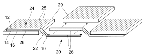
The pre-tinned connector for PV cells 29 (Figs. 4 and 5) is a strip 10 with a
flat cross-
section and a first, top broad side 12 and a second, bottom broad side 14 as
well as two
narrow sides 16, each of which connects the opposite edges of the broad sides
12, 14.
The cross-section of the strip 10 is 1 mm wide and 0.1 mm high (Fig. 1). The
strip 10 has
a copper core and on its top and bottom broad sides 12, 14 a thin layer of
silver to improve
electrical conductivity and reflection capability. The layer of silver is not
shown in the
drawings.
CA 02749423 2011-08-15
11
While the bottom broad side 14 is smooth, the top broad side 12 has a
corrugated
structure 18 with a triangular profile (Fig. 1) with an angle a of 1200 at the
peak and in the
trough. The peak-to-peak distance in the corrugated structure 18 is 150 pm and
the depth
of the corrugated structure is accordingly approximately 40 pm. The strip is
intended for a
PV connector for six-inch cells and is thus 305.5 mm long. It is divided into
three areas. In
a first area 20, 145 mm long, the strip is pre-tinned on the top broad side 12
which holds
the corrugated structure 18, and the corrugated structure 18 is filled with
the soldering tin
26 such that viewed from the outside the strip 10 in the first area 20 is
almost smooth. The
soldering tin 26 actually stands a few micrometers higher than the peaks of
the corrugated
structure 18. An intermediate area 22, in which the strip 10 is not tinned
either on the top
broad side 12 or on the bottom broad side 14, joins onto the first area 20.
The
intermediate area 22, which acts as connection area, is 15 mm long. A second
area 24,
which again is 145 mm long and which has a pre-tinned bottom broad side 14,
joins onto
it. The thickness of the pre-tinning is approximately 10 pm. Including a
cutting tolerance of
0.5 mm, the length of the strip 10 is thus 305.5 mm.
The length of the first and second areas 20, 24 is somewhat less than the
length of the
edge of a six-inch cell (Figs. 4 and 5). The connection area 22 corresponds to
the distance
between two PV cells 29 within a module. The bottom broad side 14 of the
second area 24
is soldered to the top of a PV cell 29 with the result that a connection to
the individual
contact fingers 25 of the PV cell 29 forms. As the PV cells 29 are connected
in series, the
first area 20, in which the corrugated structures 18 are completely filled
with soldering tin
26, is soldered to the bottom of the adjacent PV cell 29, with the result that
there is
likewise contact with the contact fingers. The second area 24 of the next
connector, the
first area 20 of which is again soldered to the bottom of the next-but-one PV
cell 29, is
then soldered onto the top of this PV cell 29. In this way a majority of PV
cells is
connected in series.
The pre-tinned connectors for PV cells with a corrugated structure on one side
are
produced in four steps (Fig. 6):
In a first step a copper foil or ribbon 30, 0.1 mm thick and 30 mm wide, is
guided through a
first roll gap 32, the top work roll 34 of which has circumferential
protruding wedge-shaped
ribs 36 spaced 1 mm apart, which emboss corresponding wedge-shaped notches 38
into
CA 02749423 2011-08-15
12
the copper foil 30 to a depth of 60 pm (Fig. 7), with the result that lines of
weakness 40
form (Figs. 6 and 8). The bottom work roll 42 is smooth. The material of the
copper foil 30
is slightly squeezed out at the edges of the notches 38 and thus ridges form.
The copper
foil 30 is therefore smoothed again in a second roll gap 44 with smooth work
rolls. The
wedge-shaped notches 38 are largely closed again but the lines of weakness 40
remain
and form break-off lines (Fig. 8).
In a second step the copper foil 30 is guided through a third roll gap 46, the
top work roll
48 of which has a surface with a corrugated structure 50 with a peak-to-peak
distance of
150 pm and a depth of approximately 40 pm (Fig. 9). The corrugated structure
50 has
longitudinal crests or peaks and troughs. The angle a at the crests and in the
troughs of
the corrugated structure 50 is 120 . The bottom work roll 52 of the third roll
gap 46 is
smooth. In the third roll gap 46 the corrugated structure 50 of the top roll
48 embosses the
corresponding corrugated structure 18 into the copper foil 30. The copper foil
30 is
introduced into the third roll gap 46 such that the lines of weakness 40
coincide with a
crest of the corrugated structure 50 of the top work roll 48 and accordingly
with a trough of
the corrugated structure 18 embossed into the copper foil 30.
In a third production step those sections of surface of the copper foil 30
which later
become the first areas 20 of the top broad side 12 and the second areas 24 of
the bottom
broad side 14 of the connector which are soldered to the PV cells 29 are then
pre-tinned.
For this, soldering tin is applied to the copper foil 30 in the form of solder
preforms 54 (Fig.
6). The soldering flux necessary for the tinning has been applied to the
solder preforms 54
or onto the ribbon 10 in advance. The solder preforms 54 are connected to the
copper foil
by means of a three-stage method. In the first stage 55 the solder preforms 54
are
temporarily attached by pointwise hot embossing by means of a first hot
embossing head
25 66 which has two embossing stamps. A pre-cut solder preform 54 is placed
in position and
held on the temporarily attached copper foil 30 by means of a suction gripper.
The suction
gripper has two spaced recesses through which the two dies of the first hot
embossing
head 66 travel and at these points temporarily attach the solder preform 54 to
the copper
foil 30 by heat and pressure. The copper foil 30 with the temporarily attached
solder
30 preform 54 is then clocked further and in the second stage 56 the solder
preforms 54 are
again pressed over their whole surface by hot embossing by means of a second
hot
CA 02749423 2011-08-15
13
embossing head 68. The copper foil 30 with the pressed solder preform 54 is
then clocked
further again and in the third stage the temporarily attached solder preforms
54 that have
been pressed over their whole surface are melted on by means of an infrared
radiator 70.
The solder preforms 54 are strips of soldering tin, the width of which is
somewhat less
than the 156-mm length of the edge of a six-inch PV cell at 145 mm. The
soldering tin
strips 54 are laid transverse to the corrugated structure 18 of the copper
foil 30.
In a fourth production step the corrugated copper foil 30, pre-tinned in
transverse strips, is
split into narrow ribbons of foil 58 along the lines of weakness 40. For this,
the copper foil
30 is guided through a fourth roll gap 60 with smooth work rolls which exert
no, or only a
minimal, pressure on the foil 30. A fixed separating roll 62 is arranged as
separator after
the roll gap, and adjacent foil ribbons 58 are alternately guided over and
under the
separating roll 62 and separated from one another along the lines of weakness
40. Each
thus-obtained foil ribbon 58 is then wound onto a cross-wound roll 64.
If the copper foil 30 is not to have lines of weakness 40, the first and
second roll gaps 32,
44 are omitted. The copper foil 30, provided with the corrugated structure 18
and pre-
tinned, is then divided into the foil ribbons 58 by means of roll slitters.
As the first two and the fourth production step proceed continuously, while
the metal foil 30
is moved forwards in steps in the third production step, the pre-tinning, the
metal foil 30 is
wound up after the first two production steps and then unwound for the third
production
step. Likewise it is wound up after the third production step and then unwound
again for
the fourth production step. The interim winding up is shown in Fig. 6 by the
breaks in the
line representing the copper foil 30. The copper foil 30 can also be
temporarily wound up
after passing through the first and second roll gap 32, 44.
The strips 10 of the PV cell connectors usually have a corrugated structure 18
on the
bottom and top broad side 12, 14. To produce such a PV cell connector the
bottom roll 42
of the first roll gap 32 then also has a corrugated structure 50. Areas of
both broad sides
of the metal foil 30 are then usually tinned. The tinned areas of the top
broad side 12 and
bottom broad side 14 of the metal foil 30 do not overlap, but are separated in
longitudinal
direction by a gap which alternately roughly corresponds to the distance
between two PV
cells 29 to be connected to one another and a cutting tolerance of 0.5 mm.
CA 02749423 2011-08-15
14
Both sides of the metal foil 30 can also be tinned over their whole surface.
PV cell
connectors cut out from this can then be used for PV cells of any size.
However, the
advantageous reflection properties are then lost. Expediently therefore at
least one side of
the metal foil 30 should be tinned only in the areas which, after division
into PV cell
connectors, form the first areas 20 of the top broad side 12 of the PV cell
connectors with
which this is soldered to the bottom of a PV cell 29.
The foil ribbons 58 are a series of pre-tinned strips 10 (Fig. 10) according
to the invention.
The pre-tinned first areas 20 are on the top broad side 12 and the pre-tinned
second areas
24 are on the bottom broad side 14 of each of the strips 10. The individual
strips 10 are
separated only by the cutting tolerance 28 of 0.5 mm. The first and second
areas 20, 24
on opposite sides of the ribbon 58 are separated by the intermediate areas 22
within the
strips 10 in its longitudinal direction.
CA 02749423 2011-08-15
List of reference numbers
10 strip 42 bottom work roll
12 top broad side 44 second roll gap
14 bottom broad side 46 third roll gap
16 narrow side 48 top work roll
18 corrugated structure of strip/foil 50 corrugated structure of the roll
first area 52 bottom work roll
22 intermediate area 54 solder preforms
24 second area 55 first stage (pointwise hot embossing)
contact finger 56 second stage (whole-surface hot
26 soldering tin embossing)
28 cutting tolerance 57 third stage (melting on)
29 PV cell 58 foil ribbons
copper foil 60 fourth roll gap
32 first roll gap 62 separating roll
34 top work roll 64 roll
36 ribs 66 first hot embossing head
38 notches 68 second hot embossing head
lines of weakness 70 infrared radiator