Note: Descriptions are shown in the official language in which they were submitted.
CA 02749460 2011-08-16
NEAR-FIELD COMMUNICATION (NFC) SYSTEM PROVIDING LOW POWER MODE
FREQUENCY CYCLING AND RELATED METHODS
Technical Field
[0001] This application relates to the field of
communications, and more particularly, to mobile wireless
communications devices and related methods that use Near Field
Communication (NFC).
Background
[0002] Mobile communication systems continue to grow in
popularity and have become an integral part of both personal and
business communications. Various mobile devices now incorporate
Personal Digital Assistant (PDA) features such as calendars,
address books, task lists, calculators, memo and writing
programs, media players, games, etc. These multi-function
devices usually allow electronic mail (email) messages to be
sent and received wirelessly, as well as access the internet via
a cellular network and/or a wireless local area network (WLAN),
for example.
[0003] Some mobile devices incorporate contactless card
technology and/or Near Field Communication (NFC) chips. NFC
technology may be used for contactless short-range
communications based on radio frequency identification (RFID)
standards, using magnetic field induction to enable
communication between electronic devices, including mobile
wireless communications devices. These short-range
communications may include payment and ticketing, electronic
keys, identification, device set-up service and similar
information sharing. This short-range high frequency wireless
CA 02749460 2011-08-16
communications technology may exchange data between devices over
a short distance, such as only a few centimeters.
Brief Description of the Drawings
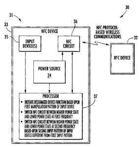
[0004] FIG. 1 is a schematic block diagram of a Near Field
Communication (NFC) system in accordance with an example aspect
providing NFC power state switching.
[0005] FIG. 2 is a front view of an NFC-enabled cellular
device which may be used in accordance with an example aspect to
implement the NFC power state switching.
[0006] FIGS. 3 and 4 are example screen prints which may be
provided on a display of the mobile device of FIG. 2 upon
implementation of NFC power state switching.
[0007] FIG. 5. is a schematic block diagram of an example NFC
device of the system of FIG. 1 shown in greater detail.
[0008] FIGS. 6 and 7 are flow diagrams illustrating NFC power
switching method aspects associated with the system or devices
of FIG. 1.
[0009] FIG. 8 is a schematic block diagram of an alternative
NFC system in accordance with an example aspect providing
synchronized peer-to-peer recognition features.
[0010] FIG. 9 is a schematic block diagram of an example NFC
device of the system of FIG. 8 shown in greater detail.
[0011] FIG. 10 is a flow diagram illustrating synchronized
NFC peer-to-peer recognition method steps associated with the
system or devices of FIG. 8.
[0012] FIGS. 11 and 12 are signal timing diagrams
illustrating signal synchronization operations performed by the
devices of the system of FIG. 8.
[0013] FIG. 13 is a schematic block diagram of an example
mobile wireless communications device providing enhanced NFC
2
CA 02749460 2011-08-16
power saving mode switching in accordance with another example
embodiment.
[0014] FIGS. 14 and 15 are schematic block diagrams of
example alternative embodiments of the mobile wireless
communications device of FIG. 13.
[0015] FIG. 16 is a flow diagram illustrating method aspects
associated with the system of FIG. 13.
[0016] FIG. 17 is a schematic block diagram illustrating
example components of a mobile wireless communications device
that may be used in accordance with the systems of FIGS. 1, 8,
or 13.
Detailed Description
[0017] The present description is made with reference to the
accompanying drawings, in which preferred embodiments are shown.
However, many different embodiments may be used, and thus the
description should not be construed as limited to the
embodiments set forth herein. Rather, these embodiments are
provided so that this disclosure will be thorough and complete.
Like numbers refer to like elements throughout.
[0018] Generally speaking, a near-field communication (NFC)
system is disclosed herein which may include a plurality of NFC
devices each including a housing, a power source carried by the
housing, at least one input device carried by the housing and
assigned to a designated device function, an NFC circuit
configured to wirelessly communicate using an NFC communications
protocol, and a processor carried by the housing and coupled to
the power source, the at least one input device, and the NFC
circuit. The processor may be configured to initiate the
designated device function based upon a first input pattern of
the at least one input device, and switch the NFC circuit
between a higher power state and a lower power state at a first
frequency, where the NFC circuit in the higher power state may
3
CA 02749460 2011-08-16
be configured to generate a radio frequency (RF) field to
initiate NFC communications with another one of the NFC devices,
and switch the NFC circuit between the higher power state and
the lower power state at a second frequency different than the
first frequency based upon a second input pattern of the at
least one input device different from the first input pattern.
As such, the system may thereby provide desired NFC device
recognition without undue delay, yet while still maintaining
power savings from low-power operation.
[0019] The processor may be further configured to switch the
NFC circuit from the second frequency back to the first
frequency based upon a repetition of the second input pattern of
the at least one input device. Also, the processor may be
configured to switch the NFC circuit from the second frequency
back to the first frequency after a timeout period. By way of
example, the first frequency may be lower than the second
frequency.
[0020] The NFC system may further include a display carried
by the portable housing and coupled to the processor. As such,
the processor may be further configured to generate on the
display a menu for enabling initiation of NFC communications
with the other NFC device upon detection thereof. By way of
example, the at least one input device may comprise a menu key,
and the designated device function may comprise generating a
menu on the display. Other example input devices may include an
audio input transducer, an accelerometer, etc. Additionally, the
processor may be further configured to pass through a Uniform
Resource Locator when at the second frequency and being in the
higher power state.
[0021] A related NFC device may include a housing, a power
source carried by the housing, at least one input device carried
by the housing and assigned to a designated device function, an
4
CA 02749460 2011-08-16
NFC circuit configured to wirelessly communicate using an NFC
communications protocol, and a processor carried by the housing
and coupled to the power source, the at least one input device,
and the NFC circuit. The processor may be configured to initiate
the designated device function based upon a first input pattern
of the at least one input device, and switch the NFC circuit
between a higher power state and a lower power state at a first
frequency, where the NFC circuit in the higher power state may
be configured to generate a radio frequency (RF) field to
initiate NFC communications with another NFC device. The
processor may also be configured to switch the NFC circuit
between the higher power state and the lower power state at a
second frequency different than the first frequency based upon a
second input pattern of the at least one input device different
from the first input pattern.
[0022] A related NFC method is for an NFC device, such as the
one described briefly above, and may include initiating the
designated device function based upon a first manipulation
pattern of the at least one input device, and switching the NFC
circuit between a higher power state and a lower power state at
a first frequency, where the NFC circuit in the higher power
state may be configured to generate a radio frequency (RF) field
to initiate NFC communications with another NFC device. The
method may further include switching the NFC circuit between the
higher power state and the lower power state at a second
frequency different than the first frequency based upon a second
input pattern of the at least one input device different from
the first input pattern.
[0023] A physical computer-readable medium having computer-
executable instructions for causing an NFC device, such as the
one described briefly above, to perform steps comprising
initiating the designated device function based upon a first
CA 02749460 2011-08-16
manipulation pattern of the at least one input device, and
switching the NFC circuit between a higher power state and a
lower power state at a first frequency, where the NFC circuit in
the higher power state may be configured to generate a radio
frequency (RF) field to initiate NFC communications with another
NFC device. A further step may include switching the NFC circuit
between the higher power state and the lower power state at a
second frequency different than the first frequency based upon a
second input pattern of the at least one input device different
from the first input pattern.
[0024] Turning now to FIGS. 1 and 2, by way of background,
NFC is a short-range wireless communications technology in which
NFC-enabled devices are "swiped," "bumped" or otherwise moved in
close proximity to communicate. In one non-limiting example
implementation, NFC may operate at 13.56 MHz and with an
effective range of about 10cm, but other suitable versions of
near-field communication which may have different operating
frequencies, effective ranges, etc., for example, may also be
used.
[0025] NFC circuitry draws power when it is searching for
other devices or contactless cards/tags in its vicinity. Because
of privacy and security concerns, in the case of an NFC-enabled
phone, it may be desirable that the device not always respond to
a NFC reader that tries to charge/read the virtual card in the
phone. Rather, it may be desirable that the NFC device require
an action before it turns on the NFC feature and responds to
readers. One such action is to require a password to be entered
to activate an NFC search/recognition mode. However, entering a
password may be inconvenient, time-consuming, or impractical in
some circumstances. For example, when a user wants to pay for
transit in a crowded subway station, it may not be practical to
perform steps such as typing in a password, finding the NFC icon
6
CA 02749460 2011-08-16
on the device, activating the NFC icon, etc. This problem may be
exacerbated if the phone is in a locked mode, adding yet another
step to be performed (i.e., unlocking the device) to place the
device in the NFC recognition mode.
[0026] Another approach may be to have a separate or
designated key for activating the NFC functionality. However,
the space (i.e., "real estate") required for a separate,
designated key to enable an NFC operational or recognition mode
may be difficult to come by in many wireless communications
devices. That is, with the ever-increasing amount of
functionality implemented in such devices, along with the
competing desire for smaller form factors, allotting the
necessary real estate for such a designated NFC key simply may
not be practical. Moreover, the additional cost of providing a
designated key on the device may also be a drawback.
[0027] In accordance with a first aspect, an NFC system 30
illustratively includes an NFC device 31 which advantageously
addresses these technical problems. More particularly, in the
example embodiment the NFC system 30 illustratively includes a
plurality of NFC devices, namely the NFC device 31 and a second
NFC device 32. The NFC device 31 illustratively includes a
housing 33, a power source 34 carried by the housing 33, one or
more input keys 35 carried by the housing 33 and assigned to a
designated device function, and an NFC circuit 36 configured to
wirelessly communicate using an NFC communications protocol. The
NFC device 31 further illustratively includes a processor 37
carried by the housing 33 which is coupled to the power source
34, the input key 35, and the NFC circuit 36. The device 32 may
also include similar components to those described herein with
reference to the NFC device 31, but need not in all embodiments.
[0028] The NFC device 31 as shown in FIGS. 2 and 5 comprises
a mobile wireless communications device (also referred to herein
7
CA 02749460 2011-08-16
as a "mobile device") cellular smart phone enabled for NFC
communications by the NFC circuit 36. In this example
embodiment, the NFC device 31 illustratively includes an off-
hook key 40 (i.e., for initiating a phone call), a return key 42
for escaping a selection or navigating back through a menu, and
an on-hook/power key 43, which may be used for disconnecting a
phone call as for turning the NFC device 31 on or off by holding
the key down for a designated period of time. As used herein,
the term "key" means an input device that is pressed or actuated
to initiate a device function or provide an input, including
buttons, keypad keys, trackballs, scroll wheels, etc. It should
also be noted that a display 38 of the NFC device 31 shown in
FIG. 2 may be a touch screen display, and in such embodiments
the input keys 35 used to initiate the NFC operations described
herein may advantageously be touch screen keys.
[0029] Moreover, the NFC device 31 further illustratively
includes a cellular transceiver 45 carried by the housing 33 and
coupled to the power source 34 and the processor 37.
Furthermore, the processor 37 may also be configured for
communicating wireless voice and data via the cellular
transceiver 45 via a cellular communications network
(represented as a cellular tower 47 in FIG. 5), as will be
described further below. By way of example, the data
communications may include email messages, as shown in FIG. 5,
although other data (e.g., Web data, etc.) may also be
communicated. Furthermore, in some embodiments the NFC device 31
may in addition (or instead) include other types of wireless
communications circuits capable of transmitting voice or other
data, such as a wireless LAN, WiMAX, etc., circuit.
[0030] In the present example, the input key 35 which is used
for initiating NFC operations as described further below is a
menu key for generating navigation menus on the display 38. That
8
CA 02749460 2011-08-16
is, the designated device function of the input (i.e., menu) key
35 is generating navigation menus, and this designated function
is typically performed when the input key 35 is depressed once.
Other input devices may also be used in some embodiments, such
as an audio input device (e.g., microphone), accelerometer, etc.
[0031] Operation of the processor 37 and the advantageous NFC
power state switching features performed thereby will now be
described with reference to FIGS. 6 and 7. Beginning at Block
60, the processor 37 is advantageously configured to initiate
the designated device function (menu generation in the present
example) based upon a first input or manipulation pattern of the
input key 35, at Blocks 61-62. As noted above, this first
manipulation pattern comprises a single actuation of the input
key 35, although a first different actuation pattern may be used
in other embodiments. Moreover, a different input key may be
selected for initiation of NFC operations, such as the on-hook
key 43, a side convenience key designated for a different
designated device function, etc. Furthermore, more than one such
key may be designated to initiate the same NFC functionality.
[0032] The processor 37 is further configured to switch the
NFC circuit 36 between a higher power state and a lower power
state at a first frequency, at Block 63. More particularly, this
operation would correspond to a typical low power mode as
specified by the above-described NFC standard materials, in
which the NFC circuit 36 cycles on (high power) and off (low
power), usually every three seconds. Such power cycling is
advantageous because in the high power state, the NFC circuit 36
is configured to generate a radio frequency (RF) field to
initiate NFC communications with the other NFC device 32. To
leave this field on continuously in the NFC device 31 where the
power source 34 is a battery (as seen in the more detailed view
of the NFC device 31 illustrated in FIG. 5) would deplete the
9
CA 02749460 2011-08-16
battery at an undesirable rate, which is why the low power
recognition mode may be used.
[0033] Yet, a difficultly with the standard low power mode is
that three seconds is a relatively long time in terms of NFC
communications to wait for device recognition to occur, and may
not be practical for some applications which require relatively
quick acquisition and recognition. Thus, in some embodiments,
the processor 37 may also advantageously be configured to switch
the NFC circuit 36 between the higher power state and the lower
power state at a second frequency different than the first
frequency based upon a second manipulation pattern of the input
key 35 different from the first manipulation pattern, at Blocks
64-65, thus concluding the method illustrated in FIG. 6 (Block
66).
[0034] By way of example, the second manipulation pattern may
include multiple (e.g., two) actuations or pressings of the
input key 35 in succession, i.e., within a threshold period or
window of time (e.g., one second or less). Moreover, the second
frequency may be faster than the first frequency, e.g., about
one second (or less), which is three times faster than the
above-noted first frequency of three seconds. However, in
different embodiments the first and second frequencies may take
other values besides those example values set forth herein. As
such, the NFC device 31 advantageously provides desired NFC
device recognition without undue delay, yet while still
maintaining power savings from low-power operation.
[0035] The processor 37 may be further advantageously
configured to switch the NFC circuit 36 from the second
frequency back to the first frequency based on a repetition of
the second manipulation pattern of the input key 35, at Block
72' (FIG. 7) . For example, it may be desirable to switch the
NFC device 31 to the second frequency when approaching an NFC
CA 02749460 2011-08-16
tag/reader (e.g., a subway or ticket kiosk, etc.) and quick
recognition is required, but to switch back when no longer in
proximity of the NFC tag/reader to save power, as well as for
security reasons.
[0036] In this regard, when the second manipulation pattern
occurs and power is cycled to the NFC circuit 36 at the second
frequency, this may indicate to the processor 37 that the NFC
device 31 is in proximate to a trusted NFC device, and therefore
the processor 37 may temporarily lessen security requirements
when authorizing and communicating with the trusted NFC device.
For example, the processor 37 may proceed directly to
communicate with the trusted NFC device, and in the case of a
"smart poster" NFC device, such as one configured to pass a
Uniform Resource Locator (URL), the processor 37 may
automatically direct a browser application thereof to the URL
without prompting for permission to proceed to the designated
location, at Blocks 70'-71'.
[0037] For the same reasons, the processor 37 may be
configured to switch the NFC circuit 36 from the second
frequency back to the first frequency after a timeout period, at
Block 73' . In other words, the processor 37 may perform an
automatic switching back to the first frequency based upon the
timeout condition, in addition to, or instead of, the manual
switch back described above (i.e., resulting from the second
manipulation pattern being initiated again).
[0038] Example menus 50, 51 that may be generated by the
input (i.e., menu) key 35 are respectively shown in FIGS. 3 and
4. More particularly, the menu 50 is generated by the processor
37 when the NFC device 31 is in a normal operating mode and the
input key 35 is actuated. In some embodiments, if the display 38
is not illuminated, a first actuation may initially illuminate
the display, and a subsequent actuation may then generate the
11
CA 02749460 2011-08-16
menu 50. The menu options provided by the processor 37 in the
menu 50 may vary depending upon the various operations being
performed by the device (e.g., the menu generated on a "home"
screen will be different than the one generated while an email
application is open, etc.). In the illustrated example, upon
initiation of the first manipulation pattern the menu 50
includes the following options: move, move to folder, hide,
delete, add folder, and switch application. So, in the present
example, the menu 50 would be displayed upon a first actuation
or pressing of the input key 35.
[0039] However, when the second manipulation pattern of the
input key 35 is detected, i.e., a double tap or second
actuation/pressing of the input key 35, then the processor 37
causes switching of the NFC circuit 36 based upon the second
frequency, which is indicated by an arrow extending from the
menu 50 and notation that this NFC operational mode has been
enabled for thirty seconds. However, it should be noted that
other timeout periods greater or lesser than thirty seconds may
be used in some embodiments (e.g., one minute, two minutes,
etc.), and in other embodiments the timeout period may not be
used at all.
[0040] Turning to the menu 51, here the processor 37
generates a menu on the display 38 for enabling initiation of
NFC device recognition and communications with the other NFC
device 32 upon detection thereof from a "locked" device mode.
That is, the menu 51 is generated from the locked mode, meaning
that the keypad (whether touch screen or individual buttons) or
other convenience keys are disabled by the processor 37. In some
locked modes, the display 38 may be changed to a default image
as well (e.g., a blank screen with only a background color/image
and no icons). In this case, the menu 51 generated by the
processor 37 may advantageously be different than the menu 50,
12
CA 02749460 2011-08-16
since there is a relatively small selection of operations that
may be performed from the locked mode. So, when in the locked
mode and the input key 35 is actuated once, the menu 51 is
displayed and illustratively includes the following options:
enable NFC for thirty seconds; unlock; emergency call; and
cancel. The "enable NFC for 30s" option is highlighted so that
upon a second actuation of the input key 35 this option is
automatically selected, again causing the processor 37 to
implement switching at the second frequency. While this menu
option may also be selected directly on the touch screen display
38, a second actuation of the input key 35 typically may be
performed much easier and faster.
[0041] The NFC device 31 therefore advantageously provides a
relatively convenient and consistent way of enabling the NFC
circuit 36 for a short period of time, which may be particularly
helpful for applications with relatively low security
requirements, or for relatively low-value payment transactions.
The above-described implementation further advantageously
utilizes an existing input key 35 on the NFC device 31 and
provides for relatively easy access to enable NFC
communications.
[0042] A related physical, computer-readable medium may have
computer-executable instructions for causing the NFC device 31
to perform steps including initiating the designated device
function based upon a first manipulation pattern of the input
key 35, and switching the NFC circuit 36 between a higher power
state and a lower power state at a first frequency, as discussed
above. Moreover, a further step may include switching the NFC
circuit 36 between the higher power state and the lower power
state at a second frequency different than the first frequency
based upon a second manipulation pattern of the input key 35
13
CA 02749460 2011-08-16
different from the first manipulation pattern, again as further
discussed above.
[0043] Turning now to FIGS. 8-12, another drawback of the
existing NFC lower-power tag detection approach is that it does
not work in conjunction with a peer-to-peer NFC mode. In
accordance with another advantageous aspect, an NFC system 130
and NFC devices 131, 132 advantageously provide a low power
operation when in a peer-to-peer operating mode. That is, in the
NFC system 130 both devices 131, 132 are operational in a peer-
to-peer NFC mode.
[0044] The various components illustrated in FIGS. 8 and 9
that correspond to those previously discussed above with
reference to FIGS. 1 and 2 are numbered in increments of decades
(i.e., the power source 34 is similar to the power source 134,
etc.) for clarity of reference. As such, to the extent these
components have already been explained above that explanation
will not be repeated here, and the following discussion will
accordingly focus on the additional operations performed by such
components in accordance with the present example.
[0045] Beginning at Block 200, the processor 137 is
advantageously configured to synchronize or temporally align an
internal timing signal I (i.e., a local timing signal)#to an
external timing signal E, at Block 201. The internal timing
signal I is shown initially out of synchronization with the
external timing signal E in FIG. 11, and FIG. 12 shown the
internal timing signal I' after synchronization with the
external timing signal E. It should be noted that the internal
and external signals I, E need not be mirror images of one
another to be synchronized as shown in FIG. 12, but may be
synchronized in the sense that leading or trailing edges are
temporally aligned (e.g., the signals could be inverted with
respect to one another but still synchronized in time).
14
CA 02749460 2011-08-16
[0046] The internal timing signal I may be generated by the
processor 137 using a variety of techniques. Furthermore, the
external timing signal E may be obtained from a number of
different sources, as seen in FIG. 9. For example, the processor
137 may be configured to synchronize the internal timing signal
I to a cellular network timing signal as the external timing
signal E via the cellular transceiver 145. In accordance with
another option, each NFC device 131, 132 may further include a
satellite positioning receiver 146 coupled to the processor 137
and configured to receive a satellite positioning system (e.g.,
GPS, Galileo, GLONASS, etc.) timing signal from one or more
satellites 147, with which the processor 137 is configured to
synchronize the internal timing signal to as the external timing
signal I. Still another option is that the processor 137 may be
configured to synchronize the internal timing signal I to the
common external system timing signal E via the NFC circuit 136
(e.g., synchronization to GMT or other accurate time source via
NFC communications, etc.).
[0047] The processor 137 is further configured to cycle power
to the NFC circuit 136 to periodically switch the NFC circuit
136 between a peer-to-peer recognition state and a low power
state based upon the synchronized internal timing signal I, at
Block 202. When NFC devices are powered up and operating in a
peer-to-peer mode, they continuously generate an RF field for
recognizing and communicating with other NFC devices. However,
because each of the devices 131, 132 is synchronized to the same
external timing signal and performs the power cycling at the
same intervals, they advantageously generate their respective RF
fields and perform device recognition at the same times, and
thus these devices will be able to "see" each other despite now
operating in a power saving mode.
CA 02749460 2011-08-16
[0048] Thus, the processor 137 of the device 131 is also
advantageously configured to initiate peer-to-peer NFC
communications with the other device 132 when in range thereof
upon being switched (e.g., simultaneously switched) to the peer-
to-peer recognition state therewith, at Blocks 203-204, thus
concluding the method illustrated in FIG. 10 (Block 205) . As
such, the system advantageously addresses the technical problem
of providing a relatively low-power NFC peer-to-peer recognition
mode, while still providing desired recognition times without
undue delay.
[0049] The processor 137 may further be configured to operate
the NFC circuit 136 in an active communication mode in the peer-
to-peer recognition state. Furthermore, the processor 137 may be
configured to cycle power to the NFC circuit 136 at various time
intervals, although an interval of not greater than one second
may be desirable, as shorter durations may be particularly
beneficial from a rapid recognition standpoint, such as in the
range of approximately 200 ps to approximately 600 ps, for
example, although other durations may be used in different
embodiments. Generally speaking, the interval is balanced to be
long enough to provide desired power savings but also quick
recognition times.
[0050] It should be noted that in the system 130, both NFC
devices 131, 132 need not be mobile wireless NFC devices. For
example, some electronic devices such as televisions, printers,
etc., may be enabled with NFC circuitry, but these devices are
essentially stationary and typically plugged in to a building
power source. As such, while power savings may not be as high a
priority for stationary or wall-powered devices, such stationary
devices may still operate as described above and be included in
the system 130 (or the system 30 in some embodiments) to
initiate NFC communications with mobile devices which utilize
16
CA 02749460 2011-08-16
these techniques to conserve battery power. Moreover, it should
also be noted that while two devices are shown in the above-
described system 30, 130 for ease of illustration, in some
embodiments more than two devices may be included in the
particular system.
[0051] A related physical computer-readable medium is also
provided and may have computer-executable instructions for
causing the NFC device 131 to perform steps including
synchronizing an internal timing signal I of the NFC device to
an external timing signal E, and cycling power to the NFC
circuit 136 to periodically switch the NFC circuit between a
peer-to-peer recognition state and a low power state based upon
the synchronized internal timing signal I'. A further step may
include initiating peer-to-peer NFC communications with another
NFC device 132 when in range thereof and upon being
simultaneously switched to the peer-to-peer recognition state
therewith.
[0052] Referring now additionally to FIGS. 13-16, in
accordance with another example embodiment a mobile device 300
illustratively includes a portable housing 301 and an NFC
circuit 302 carried by the portable housing. As discussed above,
the NFC circuit 302 may be switched between different operating
modes, including an active NFC mode, and a power saving mode,
such as a passive mode or an unpowered mode. The mobile device
300 further illustratively includes a processor 303 carried by
the portable housing 301 that is coupled to the NFC circuit 302.
Beginning at Block 350, the processor 303 is configured to
switch the NFC circuit 302 between the active NFC mode and the
power saving NFC mode at a first frequency based upon a first
triggering event, at Blocks 351-352, and switch the NFC circuit
between the active NFC mode and the power saving NFC mode at a
second frequency lower than the first frequency based upon a
17
CA 02749460 2011-08-16
second triggering event different than the first triggering
event, at Blocks 353-354, thus concluding the method illustrated
in FIG. 16 (Block 355) . By way of example, this may be done by
setting the active NFC mode "on" or "burst" time to a given or
fixed duration, and changing the power saving NFC mode time
between bursts. That is, the processor 303 may cycle the NFC
circuit 302 to the active NFC burst mode with longer or shorter
power saving NFC mode durations therebetween. Generally
speaking, the duration of the active mode pulse should be long
enough to recognize a load on the electromagnetic field, such as
about 60 is, although other durations may also be used.
[0053] Generally speaking, the first triggering event may be
an action or operation which indicates that the mobile device
300 is in use. In the example shown in FIG. 14, the mobile
device 300' includes a display 304', and one triggering event
that may indicate the mobile device is in use (i.e., a first
triggering event) is when the display is illuminated.
Conversely, a second triggering event which is indicative of the
mobile device 300' not being in use is when the display 304' is
not illuminated, i.e., it is in a non-illuminated or "sleep"
mode. By way of example, the first frequency may be five or more
times per second, whereas the second frequency may be less than
five times a second (e.g., once per second), although other
values for these frequencies may also be used in different
embodiments. Moreover, subsequent triggers may optionally be
used to further decrease the active mode cycling frequency, or
turn off the active mode indefinitely in some implementations.
[0054] In some embodiments the display 304' may be
illuminated based upon a key press, etc., even if the display or
mobile device 300' is in a locked mode. Other events that may
cause the display 304' to be illuminated, or otherwise serve as
a first triggering event, include a calendar reminder generated
18
CA 02749460 2011-08-16
by a calendar application running on the mobile device 300',
receipt of a message (e.g., email, SMS, MMS, etc.) via a
wireless network, etc. By associating the frequency at which
cycling to the NFC power saving mode is performed with the
operational state of the display 304', this provides a ready
indication that if the display 304' is illuminated, then the NFC
circuit 302' is in its fastest NFC acquisition mode. The
processor 303' may be further configured to implement a delay
period or lag time after the display 304' is switched to the
non-illuminated mode. This may advantageously help reduce
situations where the display 304' goes into a sleep mode (i.e.,
the non-illuminated mode) while the NFC circuit 302' is
attempting to engage in communications with another NFC device,
which may otherwise increase the possibility of not establishing
an NFC communications link therewith if the NFC circuit 302' is
switched to the slower NFC acquisition mode. Similarly,
establishing an NFC communications link may serve as a first
triggering event that causes the processor 303' to switch
between the active NFC mode and the power saving NFC mode at the
first (i.e., faster) frequency.
[0055] In the example shown in FIG. 15, the mobile device
300" illustratively includes two input devices, namely an input
key(s) 305' ' (such as found on a keypad, a convenience key or
button, etc., as noted above) and an accelerometer 306''. Other
examples of input devices may include track balls, touch pads,
scroll wheels, biometric sensors, touch screens, etc. With
respect to a given input device, the first triggering event may
comprise an input therefrom (e.g., key press, movement detection
by accelerometer 306", etc.), while the second triggering event
may comprise exceeding a threshold period since a last input is
received. For example, if the input key 305" is not pressed or
no motion is detected by the accelerometer 306'' within the
19
CA 02749460 2011-08-16
threshold period (e.g., ten seconds), then the processor 303"
causes the NFC circuit 302'' mode cycling to occur at the
second, slower rate to thereby conserve power. Other threshold
periods may be used, and in some embodiments this threshold may
be user-selectable. Further, it should be noted that not all of
the input devices on a given mobile device need be used for NFC
mode switching purposes in all embodiments, i.e., the NFC mode
switching may be associated with one or more input devices in
different embodiments.
[0056] One particular advantage of using an input device for
triggering the change in frequency of the NFC circuit 302"
power saving mode cycling is that input from a particular key
305" or the accelerometer 306" need not "wake up" (i.e.,
illuminate) the display 304', which may help provide further
power savings if NFC communications may be performed in the
background, for example. In such embodiments, a "click" from the
key 305'' or other feedback may be used to provide a suitable
indication that the NFC mode switching frequency has been
changed without the need for visual verification on the display
304'. With respect to the accelerometer 306" , NFC
communications typically require "swiping" of another NFC
device, and therefore movement of the mobile device 300 may
be taken to mean that the device is being carried or
transported, making the first NFC mode switching frequency more
appropriate, while the second frequency would be more
appropriate when the mobile device is at rest. It should be
noted that other input devices or sensors may similarly be used
to detect when the mobile device 300' ' is held in a hand or
being moved (e.g., infrared (IR) sensor, motion sensor, image
(e.g., camera) sensor, etc.).
[0057] The mobile devices 300, 300', and 300" may further
include one or more wireless transceivers (e.g., cellular, WiFi,
CA 02749460 2011-08-16
WiMAX, etc.), and the processors 303, 303', and 303' ' may also
be configured for communicating email messages, as discussed
further above. A non-transitory computer-readable medium is also
provided for causing the NFC circuit 302 to switch between the
active NFC mode and the power saving NFC mode at a first
frequency based upon a first triggering event, and switch
between the active NFC mode and the power saving NFC mode at a
second frequency lower than the first frequency based upon a
second triggering event different than the first triggering
event, as discussed further above.
[0058] Example components of a mobile wireless communications
device 1000 that may be used in accordance with an example
embodiment are further described below with reference to FIG.
17. The device 1000 illustratively includes a housing 1200, a
keyboard or a keypad 1400 and an output device 1600. The output
device shown is a display 1600, which may comprise a full
graphic LCD. Other types of output devices may alternatively be
utilized. A processing device 1800 is contained within the
housing 1200 and is coupled between the keypad 1400 and the
display 1600. The processing device 1800 controls the operation
of the display 1600, as well as the overall operation of the
mobile device 1000, in response to actuation of keys on the
keypad 1400.
[0059] The housing 1200 may be elongated vertically, or may
take on other sizes and shapes (including clamshell housing
structures) . The keypad may include a mode selection key, or
other hardware or software for switching between text entry and
telephony entry.
[0060] In addition to the processing device 1800, other parts
of the mobile device 1000 are shown schematically in FIG. 17.
These include a communications subsystem 1001; a short-range
communications subsystem 1020; the keypad 1400 and the display
21
CA 02749460 2011-08-16
1600, along with other input/output devices 1060, 1080, 1100 and
1120; as well as memory devices 1160, 1180 and various other
device subsystems 1201. The mobile device 1000 may comprise a
two-way RF communications device having data and, optionally,
voice communications capabilities. In addition, the mobile
device 1000 may have the capability to communicate with other
computer systems via the Internet.
[0061] Operating system software executed by the processing
device 1800 is stored in a persistent store, such as the flash
memory 1160, but may be stored in other types of memory devices,
such as a read only memory (ROM) or similar storage element. In
addition, system software, specific device applications, or
parts thereof, may be temporarily loaded into a volatile store,
such as the random access memory (RAM) 1180. Communications
signals received by the mobile device may also be stored in the
RAM 1180.
[0062] The processing device 1800, in addition to its
operating system functions, enables execution of software
applications 1300A-1300N on the device 1000. A predetermined set
of applications that control basic device operations, such as
data and voice communications 1300A and 1300B, may be installed
on the device 1000 during manufacture. In addition, a personal
information manager (PIM) application may be installed during
manufacture. The PIM may be capable of organizing and managing
data items, such as e-mail, calendar events, voice mails,
appointments, and task items. The PIM application may also be
capable of sending and receiving data items via a wireless
network 1401. The PIM data items may be seamlessly integrated,
synchronized and updated via the wireless network 1401 with
corresponding data items stored or associated with a host
computer system.
22
CA 02749460 2011-08-16
[0063] Communication functions, including data and voice
communications, are performed through the communications
subsystem 1001, and possibly through the short-range
communications subsystem. The communications subsystem 1001
includes a receiver 1500, a transmitter 1520, and one or more
antennas 1540 and 1560. In addition, the communications
subsystem 1001 also includes a processing module, such as a
digital signal processor (DSP) 1580, and local oscillators (LOs)
1601. The specific design and implementation of the
communications subsystem 1001 is dependent upon the
communications network in which the mobile device 1000 is
intended to operate. For example, a mobile device 1000 may
include a communications subsystem 1001 designed to operate with
the MobitexTM, Data TACT"' or General Packet Radio Service (GPRS)
mobile data communications networks, and also designed to
operate with any of a variety of voice communications networks,
such as AMPS, TDMA, CDMA, WCDMA, PCS, GSM, EDGE, etc. Other
types of data and voice networks, both separate and integrated,
may also be utilized with the mobile device 1000. The mobile
device 1000 may also be compliant with other communications
standards such as 3GSM, 3GPP, UMTS, etc.
[0064] Network access requirements vary depending upon the
type of communication system. For example, in the Mobitex and
DataTAC networks, mobile devices are registered on the network
using a unique personal identification number or PIN associated
with each device. In GPRS networks, however, network access is
associated with a subscriber or user of a device. A GPRS device
therefore typically involves use of a subscriber identity
module, commonly referred to as a SIM card, in order to operate
on a GPRS network.
[0065] When required network registration or activation
procedures have been completed, the mobile device 1000 may send
23
CA 02749460 2011-08-16
and receive communications signals over the communication
network 1401. Signals received from the communications network
1401 by the antenna 1540 are routed to the receiver 1500, which
provides for signal amplification, frequency down conversion,
filtering, channel selection, etc., and may also provide analog
to digital conversion. Analog-to-digital conversion of the
received signal allows the DSP 1580 to perform more complex
communications functions, such as demodulation and decoding. In
a similar manner, signals to be transmitted to the network 1401
are processed (e.g. modulated and encoded) by the DSP 1580 and
are then provided to the transmitter 1520 for digital to analog
conversion, frequency up conversion, filtering, amplification
and transmission to the communication network 1401 (or networks)
via the antenna 1560.
[0066] In addition to processing communications signals, the
DSP 1580 provides for control of the receiver 1500 and the
transmitter 1520. For example, gains applied to communications
signals in the receiver 1500 and transmitter 1520 may be
adaptively controlled through automatic gain control algorithms
implemented in the DSP 1580.
[0067] In a data communications mode, a received signal, such
as a text message or web page download, is processed by the
communications subsystem 1001 and is input to the processing
device 1800. The received signal is then further processed by
the processing device 1800 for an output to the display 1600, or
alternatively to some other auxiliary I/O device 1060. A device
may also be used to compose data items, such as e-mail messages,
using the keypad 1400 and/or some other auxiliary I/O device
1060, such as a touchpad, a rocker switch, a thumb-wheel, or
some other type of input device. The composed data items may
then be transmitted over the communications network 1401 via the
communications subsystem 1001.
24
CA 02749460 2011-08-16
[0068] In a voice communications mode, overall operation of
the device is substantially similar to the data communications
mode, except that received signals are output to a speaker 1100,
and signals for transmission are generated by a microphone 1120.
Alternative voice or audio I/O subsystems, such as a voice
message recording subsystem, may also be implemented on the
device 1000. In addition, the display 1600 may also be utilized
in voice communications mode, for example to display the
identity of a calling party, the duration of a voice call, or
other voice call related information.
[0069] The short-range communications subsystem enables
communication between the mobile device 1000 and other proximate
systems or devices, which need not necessarily be similar
devices. For example, the short-range communications subsystem
may include an infrared device and associated circuits and
components, NFC or a BluetoothTM communications module to provide
for communication with similarly-enabled systems and devices.
[0070] Many modifications and other embodiments will come to
the mind of one skilled in the art having the benefit of the
teachings presented in the foregoing descriptions and the
associated drawings. Therefore, it is understood that various
modifications and embodiments are intended to be included within
the scope of the appended claims.