Note: Descriptions are shown in the official language in which they were submitted.
CA 02750896 2011-07-26
Description
Title of the Invention: SEMICONDUCTOR DRIVE DEVICE
Technical Field
[0001]
The present invention relates, in a drive circuit that
controls the turning on and off of a semiconductor device such
as an IGBT (Insulated Gate Bipolar Transistor) , to the
protection of the drive circuit when there is a short circuit
breakdown of the semiconductor device, and impedance drops.
Background Art
[0002]
Fig. 1 shows a configuration of a drive circuit using
a heretofore known technology. In the drawing, EP represents
a forward biasing power source, EN a reverse biasing power
source, Trl a forward biasing switching element, Tr2 a reverse
biasing switching element, R1 a forward biasing gate resistor,
and R2 a reverse biasing gate resistor. A final-stage driver
circuit DCC is a circuit for driving the MOSFETs Trl and Tr2
in accordance with a control signal. Herein, an IGBT (IGBT
1) is used as a semiconductor device. MOSFET is an abbreviation
of Metal Oxide Semiconductor Field Effect Transistor.
[0003]
1
CA 02750896 2011-07-26
=
With this kind of configuration, when a short circuit
breakdown occurs in the semiconductor device, there is a high
possibility of a short circuit breakdown occurring between all
terminals G1, Cl, and El of the IGBT 1. For this reason, in
the case of Fig. 1, when there is a short circuit condition
between the gate terminal Gl and emitter terminal El, the output
of the drive circuit connected between these terminals is
short-circuited, a large current determined by the forward
biasing power source EP and forward biasing gate resistor R1
continues to flow when the MOSFET Trl is turned on, and a large
current determined by the reverse biasing power source EN and
reverse biasing resistor R2 continues to flow when the MOSFET
Tr2 is turned on. With the circuit type of Fig. 1, when taking
into consideration the breakdown of the semiconductor device,
it is essential to design in such a way that this kind of current
can be tolerated, so the capacities of the biasing power sources
EP and EN and gate resistors R1 and R2 through which the current
flows increase, leading to an increase in size and an increase
in cost of the drive circuit. Furthermore, when the drive
circuit power source is shared, there also occurs a problem
in that an overcurrent in one drive circuit renders another
drive circuit inoperative.
[0004]
As a heretofore technology that ameliorates this kind
of problem, the method shown in Fig. 2 shown in Patent Document
2
CA 02750896 2011-07-26
1 is known. EP represents a forward biasing power source, EN
a reverse biasing power source, Trlaforward biasing switching
element, Tr2 a reverse biasing switching element, R1 a forward
biasing gate resistor, and R2 a reverse biasing gate resistor.
Also, Fl, F2, and F3 represent fuses, SW1 represents a forward
biasing power source short circuiting switch, and SW2
represents a reverse biasing power source EN short circuiting
switch.
[0005]
A description will be given of actions in this circuit
when a short circuit breakdown occurs in an IGBT, which is a
semiconductor device. When an IGBT 1 short circuits, and a
large current flows through a collector, the fuse Fl melts down.
Means of detecting a meltdown being provided in the fuse Fl,
when a meltdown is detected, the switches SW1 and SW2 are turned
on. When these switches are turned on, the biasing power
sources EP and EN are short circuited via the fuses F2 and F3,
and the fuses F2 and F3 melt down. Owing to these kinds of
action, the biasing semiconductor switches Trl and Tr2 are cut
off from the biasing power sources in a short time, meaning
that the large current in the drive circuit that occurs in Fig.
1 does not occur.
Patent Document 1: JP-UM-A-6-88191
Disclosure of the Invention
3
CA 02750896 2011-07-26
[0006]
As heretofore described, with the heretofore known
technology, fuses are provided in the drive circuit and, by
actively causing the fuses to melt down when the semiconductor
device breaks down, protection of the drive circuit is realized.
However, with this method, a fuse is also necessary in the
circuit through which the main current flows in order to detect
a failure of the semiconductor device, meaning that in a large
capacity device, the circuit increases in size. Also, as it
is necessary to replace each fuse after the protection is
activated, in a device with a large number of drive circuits,
a long time is needed for failure recovery. Consequently, a
problem for the invention is to detect a short circuit breakdown
of a semiconductor device without using a fuse, and protect
the drive circuit.
[0007]
In order to solve the heretofore described problem, in
the invention, a configuration is such that a first thermistor
is thermally joined to and installed in a turn-on gate resistor,
a second thermistor is thermally joined to and installed in
a turn-off gate resistor, and a current constantly flows
through the thermistors, and there is provided means which,
when the temperature of either one of the gate resistors rises,
turns off the first or second switching element by the
resistance value of the corresponding thermistor changing, and
4
CA 02750896 2011-07-26
the current changing.
[0008]
Also, in another invention, thermistors are connected
in serieswithfirstandsecondswitchingelements respectively,
and there is provided means which, when the temperature of a
thermistor rises due to an overcurrent when there is a short
circuit between the gate and emitter of an IGBT, turns off the
first or second switching element.
[0009]
As a result of this, semiconductor device fuses and fuses
that cut off the drive circuit power source are unnecessary,
and it is possible to reduce the size of the device, and to
reduce the part replacement time at a time of failure recovery.
[0010]
Furthermore, as an operation of the means of turning off
the first or second switching element is detected by a
photocoupler, and the signal is output from the drive device,
operation and display of a cutting off of the device or failure
occurrence is possible in a control circuit using the signal,
and user-friendliness improves.
Brief Description of the Drawings
[0011]
[Fig. 1] Fig. 1 is a drive circuit diagram showing a
heretofore known example.
CA 02750896 2011-07-26
[Fig. 2] Fig. 2 is a drive circuit diagram with
protection function showing a heretofore known example.
[Fig. 3] Fig. 3 is a circuit diagram showing a first
example of the invention.
[Fig. 4] Fig. 4 is an action illustration of Fig. 1.
[Fig. 5] Fig. 5 is a circuit diagram showing a second
example of the invention.
[Fig. 6] Fig. 6 is a circuit diagram showing a third
example of the invention.
[Fig. 7] Fig. 7 is a circuit diagram showing a fourth
example of the invention.
[Fig. 8] Fig. 8 is a circuit diagram showing a fifth
example of the invention.
[Fig. 9] Fig. 9 is a circuit diagram showing a sixth
example of the invention.
[Fig. 10] Fig. 10 is a circuit diagram showing a seventh
example of the invention.
[Fig. 11] Fig. 11 is a circuit diagram showing an eighth
example of the invention.
[Fig. 121 Fig. 12 is a circuit diagram showing a ninth
example of the invention.
[Fig. 13] Fig. 13 is a circuit diagram showing a tenth
example of the invention.
Best Mode for Carrying Out the Invention
6
CA 02750896 2011-07-26
[0012]
Hereafter, a description will be given, while referring
to the drawings, of an embodiment of the invention.
[Example 1]
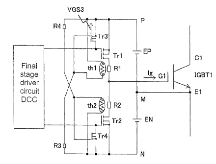
Fig. 3 shows a first example of the invention. The
difference from Fig. 1, which is a heretofore known circuit,
is that thermistors (in this example, PTC thermistors whose
resistance values increase in accordance with a temperature
rise) thl and th2 whose resistance values change depending on
the temperature are installed in gate resistors R1 and R2, the
drain and source of a P-channel type MOSFET Tr3 are connected
between the gate and source of a P-channel type MOSFET Trl,
which is a forward biasing switching element, the drain and
source of an N-channel type MOSFET Tr4 are connected between
the gate and source of an N-channel type MOSFET Tr2, which is
a reverse biasing switching element, a series circuit of the
thermistor thl and resistor R3 and a series circuit of the
thermistor th2 and resistor R4 are connected between the
positive electrode of a forward biasing power source EP and
the negative electrode of a reverse biasing power source, the
gate of the P-channel type MOSFET Tr3 is connected to the series
connection point of the thermistor thl and resistor R3, and
the gate of the N-channel type MOSFET Tr4 is connected to the
series connection point of the thermistor th2 and resistor R4.
[0013]
7
CA 02750896 2011-07-26
With this kind of configuration, when the temperature
of the turn-on gate resistor R1 rises in a condition in which
there is a short circuit failure between the gate and emitter
of an IGBT 1 and a turn-on signal is emitted, the resistance
value of the thermistor thl rises, the MOSFET Tr3 is turned
on when the voltage between the two ends of the thermistor thl
exceeds the threshold value voltage between the gate and source
of the MOSFET Tr3, and the MOSFET Trl is turned off. Also,
when the temperature of the turn-off gate resistor R2 rises
in a condition in which there is a short circuit failure between
the gate and emitter of the IGBT 1 and a turn-off signal is
emitted, the resistance value of the thermistor th2 rises, the
MOSFET Tr4 is turned on when the voltage between the two ends
of the thermistor th2 exceeds the threshold value voltage
between the gate and source of the MOSFET Tr4, and the MOSFET
Tr2 is turned off.
[0014]
Fig. 4 shows the action of each portion when a short
circuit breaking occurs between an IGBT gate and source. These
actions show a condition under which the breaking occurs with
the IGBT in a turned on condition. When the IGBT 1 is normal,
a gate current Ig has a waveform flowing for only a short time
at a time of a gate voltage rising edge or falling edge when
switching, as shown in the drawing, and the temperature of the
forward biasing gate resistor Rl is maintained at or below a
8
CA 02750896 2011-07-26
certain value. When the IGBT 1 breaks, and a short circuit
occurs between the gate (G1) and emitter (El) , a current
determined by a forward biasing power source voltage El and
the turn-on gate resistor R1 continues to flow through the
turn-on gate resistor R1, meaning that the temperature of the
R1 rises.
[0015]
Along with this, the resistance value of the thermistor
th1 increases, and a voltage VGS3 applied to the input portion
of the MOSFET Tr3 increases. When this reaches the gate
threshold value voltage of the MOSFET Tr3, the MOSFET Tr3 is
turned on, the input signal of the turn-on switching element
Tr1 becomes 0, and the Trl is turned off. Owing to this kind
of action, the current flowing in the drive circuit is
interrupted.
[0016]
At a time too of an IGBT breaking when the IGBT 1 is in
a turned off condition, that is, when the turn-off switching
element Tr2 is turned on, owing to the same kinds of action,
when the temperature of the turn-off gate resistor R2 rises,
the resistance value of the thermistor th2 increases, the
MOSFET Tr4 is turned on, and the turn-off switching element
Tr2 is turned off. As it is possible to protect the drive
circuit in this way without causing the meltdown of a fuse,
it is possible to recover the circuit without the need to
9
CA 02750896 2011-07-26
replace a part.
[0017]
[Example 2]
Fig. 5 shows a second example of the invention. The
difference from the first example is that the series circuit
of the thermistor th1 and resistor R3 is connected between the
positive electrode and negative electrode of the forward
biasing power source EP, and the series circuit of the
thermistor th2 and resistor R4 is connected between the
positive electrode and negative electrode of the reverse
biasing power source EN. By adopting this circuit
configuration, it is possible to keep the resistance and the
power consumption of the drive power sources (EP and EN) low.
[0018]
[Example 3]
Fig. 6 shows a third example of the invention. The
difference from the first example is that the P-channel type
MOSFET Tr3 is changed to a PNP transistor Q3, and the N-channel
type MOSFET Tr4 is changed to an NPN transistor Q4. The actions
are the same as in the first example, but there is an advantage
in that, by using current drive types of transistor, the noise
tolerance increases. Herein, in order to further increase the
noise tolerance, it is also possible to connect a Zener diode
or the like in series with the base.
[0019]
CA 02750896 2011-07-26
[Example 4]
Fig. 7 shows a fourth example of the invention. The
difference from the third example is that the series circuit
of the thermistor th1 and resistor R3 is connected between the
positive electrode and negative electrode of the forward
biasing power source EP, and the series circuit of the
thermistor th2 and resistor R4 is connected between the
positive electrode and negative electrode of the reverse
biasing power source EN. By adopting this circuit
configuration, it is possible to keep the resistance and the
power consumption of the drive power sources (EP and EN) low.
[0020]
[Example 5]
Fig. 8 shows a fifth example of the invention. The
difference from the first example is that a diode Dl is
connected between the drain of the P-channel type MOSFET Tr3
and the gate of the P-channel type MOSFET Trl, which is a forward
biasing switching element, a series circuit of the primary side
of a photocoupler PC1 and a resistor R6 is connected between
the series connection point of the drain of the MOSFET Tr3 and
diode Dl and the negative electrode of the reverse biasing power
source EN, a diode D2 is connected between the drain of the
N-channel type MOSFET Tr4 and the gate of the N-channel type
MOSFET Tr2, which is a reverse biasing switching element, and
a series circuit of the primary side of a photocoupler PC2 and
11
CA 02750896 2011-07-26
a resistor R5 is connected between the series connection point
of the drain of the MOSFET Tr4 and diode D2 and the positive
electrode of the forward biasing power source EP, wherein the
secondary sides of the photocouplers PC1 and PC2 are output
to the exterior as failure signals A and B. By incorporating
these signals in a control circuit or operation and display
circuit, it is possible to realize device protection, stopping,
failure display, and the like, and operability and
user-friendliness improve.
[0021]
[Example 6]
Fig. 9 shows a sixth example of the invention. The
difference from the fifth example is that the series circuit
of the primary side of the photocoupler PCl and resistor R6
and the series circuit of the primary side of the photocoupler
PC2 and resistor R5 are connected between the series connection
point of the drain of the MOSFET Tr3 and diode Dl and the negative
electrode of the forward biasing power source EP, and the series
circuit of the primary side of the photocoupler PC2 and resistor
R5 is connected between the series connection point of the drain
of the MOSFET Tr4 and diode D2 and the positive electrode of
the reverse biasing power source EN. By adopting this circuit
configuration, it is possible to keep the resistance and the
power consumption of the drive power sources (EP and EN) low.
[0022]
12
CA 02750896 2011-07-26
[Example 7]
Fig. 10 shows a seventh example of the invention. The
difference from the first example is that the first thermistor
thl is connected in series with the P-channel type MOSFET Trl,
the second thermistor th2 is connected in series with the
N-channel type MOSFET Tr2, the gate of the P-channel type MOSFET
Tr3 and the resistor R3 are connected to the series connection
point of the P-channel type MOSFET Trl and first thermistor
thl, and the gate of the N-channel type MOSFET Tr4 and the
resistor R4 are connected to the series connection point of
the N-channel type MOSFET Tr2 and second thermistor th2,
wherein, when the temperature of either one of the first
thermistor thl or second thermistor th2 rises to or above a
predetermined value, the MOSFET Tr1 or MOSFET Tr2 is turned
off. Herein, one end of the resistor R3 is connected to the
negative electrode of the reverse biasing power source EN, and
one end of the resistor R4 is connected to the positive
electrode of the forward biasing power source EP.
[0023]
When there is a short circuit failure between the gate
and emitter of the IGBT 1, the MOSFET Trl is turned on when
a turn-on signal is emitted so, as an excessive current flows
in the thermistor thl, the temperature of the thermistor thl
rises, and the resistance value increases, the result is that
the MOSFET Tr3 is turned on, the MOSFET Trl is turned off, and
13
CA 02750896 2011-07-26
the drive circuit is protected. Also, the MOSFET Tr2 is turned
on when a turn-off signal is emitted so, as an excessive current
flows in the thermistor th2, the temperature of the thermistor
th2 rises, and the resistance value increases, the result is
that the MOSFET Tr4 is turned on, the MOSFET Tr2 is turned off,
and the drive circuit is protected.
[0024]
[Example 8]
Fig. 11 shows an eighth example of the invention. The
difference from the seventh example is that one end of the
resistors R3 and R4 is connected to the negative electrode of
the forward biasing power source (the positive electrode of
the reverse biasing power source).
By adopting this configuration, as well as the loss of
the resistors R3 and R4 decreasing, it is possible to reduce
the capacity of the drive circuit power sources (EP and EN)
[0025]
[Example 9]
Fig. 12 shows a ninth example of the invention. The
difference from the seventh example is that a diode Dl is
connected between the drain of the P-channel type MOSFET Tr3
and the gate of the P-channel type MOSFET Trl, which is a forward
biasing switching element, a series circuit of the primary side
of a photocoupler PC1 and a resistor R6 is connected between
the series connection point of the drain of the MOSFET Tr3 and
14
CA 02750896 2011-07-26
diode Dl and the negative electrode of the reverse biasing power
source EN, a diode D2 is connected between the drain of the
N-channel type MOSFET Tr4 and the gate of the N-channel type
MOSFET Tr2, which is a reverse biasing switching element, and
a series circuit of the primary side of a photocoupler PC2 and
a resistor R5 is connected between the series connection point
of the drain of the MOSFET Tr4 and diode D2 and the positive
electrode of the forward biasing power source EP, wherein the
secondary sides of the photocouplers PC1 and PC2 are output
to the exterior as failure signals A and B. By incorporating
these signals in a control circuit or operation and display
circuit, it is possible to realize device protection, stopping,
failure display, and the like, and operability and
user-friendliness improve.
[0026]
[Example 10]
Fig. 13 shows a tenth example of the invention. The
difference from the ninth example is that one end of the
resistors R3 and R4 is connected to the negative electrode of
the forward biasing power source (the positive electrode of
the reverse biasing power source). By adopting this
configuration, as well as the loss of the resistors R3 and R4
decreasing, it is possible to reduce the capacity of the drive
circuit power sources (EP and EN).
[0027]
CA 02750896 2011-07-26
In the fifth example to the tenth example too, in the
same way as in the third and fourth examples, it is possible
to replace the P-channel type MOSFET Tr3 with the PNP transistor
Q3, and the N-channel type MOSFET Tr4 with the NPN transistor
Q4.
[0028]
The points heretofore described are summarized as
follows as the main point of the invention. That is, the main
point of the invention is that, when there is a short circuit
failure between the gate and emitter of a main switching element
such as an IGBT, the temperature of a turn-on gate resistor
or turn-off gate resistor is detected by a thermistor, and the
drive circuit is protected by turning off a turn-on gate drive
switching element or a turn-off gate drive switching element.
Furthermore, instead of detecting the temperature of the
turn-on gate resistor or turn-off gate resistor, a thermistor
is connected in series with the turn-on gate drive switching
element or turn-off gate drive switching element, the
resistance change corresponding to a change in temperature of
the thermistor is detected, and the drive circuit is protected
by turning off the turn-on gate drive switching element or
turn-off gate drive switching element.
Industrial Applicability
[0029]
16
CA 02750896 2011-07-26
The invention can be applied to an uninterruptible power
system, an electromotor drive inverter, a direct current power
supply unit, an induction heating device, or the like, to which
is applied a switching element such as an IGBT (Insulated Gate
Bipolar Transistor) or a MOSFET (Metal Oxide Semiconductor
Field Effect Transistor).
17