Note: Descriptions are shown in the official language in which they were submitted.
CA 02750918 2011-07-27
WO 2010/094102 PC ICA20091000131
Device for Grasping and Active Release of Micro and Nano Objects
Field of the Invention
The present invention relates to micro and nano manipulation, micro and
nanotechnologies, and automation at the micro and nano scales.
Background of the invention
Among the challenges of micro/nano manipulation, a long-standing difficulty is
the
release of grasped objects from the end effector due to strong adhesion
forces. Force
scaling causes surface forces (i.e., adhesion forces) including the capillary
force,
electrostatic force, and van der Waals force to dominate volumetric forces
(e.g., gravity).
In the pursuit of rapid, accurate release methods, several strategies have
thus far been
proposed.
Alteration of surface adhesion property between pick and place allows a single
needle
probe to manipulate micro objects (0. Fuchiwaki, A_ Ito, D. Misaki, and H.
Aoyama,
"Multi-axial micromanipulation organized by veratile micro robots and micro
tweezers,"
in ,Prot. IEEE Int. Conf Robotics Automation, Pasadena, CA, USA, May 2008, pp.
893-898). This method relies on UV-cured adhesive applied onto a substrate for
object
release.
Rolling movements of a single needle probe were used to manipulate the
adhesional
forces between pick and release, and had successfully constructed a diamond-
shaped
structure using microspheres (S. Saito, H. T. Miyazaki, T. Sato, and K.
Takahashi,
"Kinematics of mechanical and adhesional micromanipulation under a scanning
electron
microscope," J. Appl. Phys., vol. 92, pp. 5140-5149, 2002). The method
proposed by
Saito et al, however, requires a highly skilled operator to execute complex
motions and
relies on trial-error processes.
Active release methods that do not rely on substrate adhesion properties for
release were
also proposed. Electric field created by substrate -- probe potential
difference was used
to detach the object from the probe (K. Takahashi, H. Kajihara, M. Urago, S.
Saito, 'Y.
Mochimaru, and T. Onzawa, "Voltage required to detach an adhered particle by
coulomb
I
CA 02750918 2011-07-27
WO 201010941,02 PCT/CA2009/000181
interaction for micromanipulation," J. Appl. Phys., vol. 90, pp. 432-437,
2001). This
method, however, requires the substrate, probe, and object to be electrically
conductive.
Vacuum based method creates pressure differences between pick and place (W.
Zesch, M.
Bmnner, and A. Weber, "Vacuum tool for handling micro objects with a nano
robot," in
Proc. IEEE Int. Conf. Robotics Automation, Albuquerque, NM, USA, Apr. 1997,
pp.
1761-1766). This method, however, is not suitable for use within a vacuum
environment
such as inside the SEM (scanning electron microscope), which limits its
ability to
manipulate sub-micrometer objects.
Micro peltier coolers were used to form ice droplets instantaneously for
picking up micro
objects, and thawing the ice droplets to release objects (B. Lopez-Walle, M.
Gauthier, and
N. Chaillet, "Principle of a sub-merged freeze gripper for microassembly,"
IEEE
Transactions on Robotics, vol. 24, pp. 897-902, 2008). The manipulation
disclosed by
Lopez-Walle et al, however, must take place in an aqueous environment.
United States Patent No. 6,987,277 discloses a method for pick and place of
nano objects
by selectively activating spots on a passivated substrate using a scanning
probe
microscope tip, then release the nano objects onto the activated spots using
chemical and
physical binding forces. This manipulation process requires specially treated
sample and
substrate.
United States Patent No. 6,648,389 discloses a vibration-based release
microgripper for
pick and release. The fabrication process of the microgripper limits its
scaling down
capability, and the release accuracy is poor, as described in a similar,
vibration-based
design ("'. Fang and X. Tan, "A dynamic jkr model with application to
vibration release in
micromanipulation," in Proc. IEEE/RV Int. Conf Intelligent Robots and Systems,
Beijing, China, Oct. 2006, pp. 1341-1345).
United States Patent No. 7,025,619 discloses the use of mechanical sockets for
locking
two micro components together for assembly. This method requires each
component to
have a specially designed mechanical junction for assembly.
While several patented microgripper designs exist, they only focus on the
grasping
capability. There are no known gripper designs that are capable of reliable
release. For
2
CA 02750918 2011-07-27
WO 2014/094102 PCT/CA2009/000181
example, United States Patent No. 6,862,921 (Veeeo Instruments Inc.) discloses
the use
of two scanning probe microscope tips that are used in combination to form
tweezers for
manipulation; United States Patent No. 7,261,352 (Samsung Electronic Co., Ltd)
discloses a carbon nanotube gripping device. Other companies that specialize
in micro
and nanotechnologies, such as Zyvex or Nascatec, have commercialized different
types of
microgrippers and probes capable of picking up objects, but all lack release
mechanisms.
Besides the lack of release capabilities in existing designs, existing designs
also have
limited down scaling capabilities. To manipulate nanometer-sized objects, the
manipulation tip of the device ideally should have a comparable size to the
object. This is
difficult to accomplish in most fabrication processes for MEMS-based
(microelectromechanical systems) microgrippers, where all structural features
in the
device typically have the same thickness. By reducing the device thickness,
the
performance of the microactuator is greatly reduced due to decreased
overlapping areas
or volume; and the poor aspect ratio in flexures produces undesired motions
during
operation. While down scaling is easy to achieve with a needle probe, the pick-
up
capability of needle probes is very limited.
Jo summary, the lack of highly repeatable and accurate release methods limits
efficient,
automated micro and nano manipulation, which is important for in situ sample
preparation and handling as well as for the construction of micro and nano
structures/devices. What is needed is a gripper design that permits (1) easy,
secured
grasping of micro, nanometer-si2ed objects; (2) rapid, highly reproducible,
accurate
release of the objects; and (3) ready down scaling for manipulating sub-
micrometer and
nanometer sized objects.
Summary of Invention
In one aspect of the present invention, a device capable of grasping nanometer
or
micrometer sized objects and performing active release of the objects is
provided.
In another aspect of the present invention, a method of manufacturing a device
for
grasping objects and performing active release of said objects is provided.
3
CA 02750918 2011-07-27
WO 2010/094102 POT/CA2009/000181
As such, in one aspect, the present invention is a device for manipulating
nanometer-scale sized objects or micrometer-scale sized objects, characterized
in that the
device comprises:
(a) gripping arms for grasping the objects;
(b) a release plunger for actively releasing the objects from gripping arms;
and
(c) microactuation means connected to the gripping arms and the release
plunger and operable to actuate the gripping arras and said release plunger to
grasp and actively release the objects from the gripping arms.
In yet another aspect, the present invention is a method of manufacturing a
device for
manipulating nanometer-scale sized objects or micrometer-scale sized objects,
said
device comprising structural elements, said structural elements including
gripping arras
for grasping the objects, a release plunger for actively releasing the objects
from gripping
arms, and microactuation means connected to the gripping arms and the release
plunger
and operable to actuate the gripping arms and said release plunger to grasp
and actively
release the objects from the gripping arms, characterized in that said method
comprises
the following steps:
(a) providing a wafer having a top side and a bottom side, said wafer
comprising a top layer, a middle layer and a bottom layer, wherein said layers
are
made of materials having a suitable etch selectivity;
(b) patterning etching the top layer into a desired final pattern of the top
layer
corresponding to the device;
(c) etching from the top side exposed areas of the middle layer until the
bottom layer; and
(d) etching from the top side exposed areas of the bottom layer,
thereby providing the device for manipulating the objects.
In a further aspect, the present invention is a method of manufacturing a
device for
manipulating nanometer-scale sized objects or micrometer-scale sized objects,
said
4
CA 02750918 2011-07-27
WO 2010/094102 PCT/CA20091000181
device comprising structural elements, said structural elements including
gripping arms
for grasping the objects, a release plunger for actively releasing the objects
from gripping
arms, and microactuation means connected to the gripping arms and the release
plunger
and operable to actuate the gripping arms and said release plunger to grasp
and actively
release the objects from the gripping arms, wherein the gripping arms comprise
gripping
tips having a thickness and wherein said method is capable of selectively
reducing the
thickness of said tips with, respect to the structural elements, characterized
in that the
method comprises the following steps;
(a) providing a wafer having a top side and a bottom side, said wafer
comprising a top layer, a middle layer and a bottom layer, wherein said layers
are
made of materials having a suitable etch selectivity;
(b) patterning etching the top layer into a desired final pattern of the top
layer
corresponding to the device;
(c) applying onto the top layer a photoresist mask, and pattern said mask into
a desired final pattern of the middle layer corresponding to the structural
elements
of the device;
(d) etching from the top side exposed areas of the middle layer until the
bottom layer,
(e) etching from the top side exposed areas of the top layer and the bottom
layer; and
(0 etching from the top side exposed areas of the middle layer, thereby
providing the device comprising gripping tips having their thickness reduced
with
respect to the structural elements.
In yet another aspect, the present invention is a method of manufacturing a
device for
manipulating nanozneter-scale sized objects or micrometer-scale sized objects,
said
device comprising structural elements, said structural elements including
gripping arms
for grasping the objects, a release plunger for actively releasing the objects
from gripping
arms, and microactuation means connected to the gripping arms and the release
plunger
and operable to actuate the gripping arms and said release plunger to grasp
and actively
CA 02750918 2011-07-27
WO 2010/094102 PCT/CA2009/000181
release the objects from the gripping arms, characterized in that said method
comprises
patterning etching a silicon-on-insulator wafer from a single side of said
wafer.
In yet a further aspect, the present invention is a microfabrication method
enabling the
patterning of two layers of materials from a single side of a wafer in order
to manufacture
a device for manipulating nanometer-scale sized objects or micrometer-scale
sized
objects, said device comprising high-aspect-ratio structures and low-aspect-
ratio
structures, characterized in that said method comprises the following steps:
(a) providing a wafer having a top side and a bottom side, said wafer
comprising a top layer, a middle layer and a bottom layer, wherein said layers
are
made of materials having a suitable etch selectivity;
(b) patterning etching the top layer into a desired final pattern of the top
layer
corresponding to the device;
(c) applying onto the top layer a photoresist mask, and pattern said mask into
a desired final pattern of the middle layer corresponding to the high-aspect-
ratio
structures of the device;
(d) etching from the top side the exposed areas of the middle layer until the
bottom layer;
(e) etching from the top side the exposed areas of the top layer and the
bottom
layer;
(f) etching from the top side the exposed areas of the middle layer, thereby
forming the low-aspect-ratio structures of the device.
In a further aspect yet, the present invention is a method for grasping and
placing an
object to a desired target area with the use of a device capable of
manipulating
manometer-scale sized objects or micrometer-scale sized objects, said device
comprising
gripping arms capable of opening and closing around the object, a release
plunger for
actively releasing the object from the gripping arms, and microactuation means
connected
to the gripping arms and the plunger and operable to actuate said gripping
arms and
release plunger, characterized in that said method comprises the following
steps:
(a) closing the gripping arms around the object to grasp;
6
CA 02750918 2011-07-27
WO 2010/094102 PCTICA2009/000181
(b) moving the device to lift the object up and transport the object to the
desired target area;
(c) opening the gripping arms; and
(d) activating the plunger to actively release the object attached by adhesion
forces to an arm of the gripping arms thereby placing the object on the target
area.
In another aspect of the present invention, integrated, single-chip, batch
microfabricated
MEMS devices are disclosed that are electrostatically or electrothermally
driven grippers
for grasping micrometer or nanometer sized objects with two independently
actuated
gripping arms and an integrated plunger for active release of the objects. The
plunger is
capable of impacting or pushing the objects and allows the adhered objects to
gain
sufficient momentum to overcome the adhesion forces and enables release on
demand.
Advantages of the present invention include a device for grasping and actively
releasing
objects having a design that permits (1) easy, secured grasping of micro or
manometer-sized objects; (2) rapid, highly reproducible, accurate release of
the objects in
target areas; and (3) precise down scaling of the mxicrogripping tip for
manipulating
sub-micrometer and nanometer sized objects.
Brief Description of the Drawines
A detailed description of one or more embodiments is provided herein below by
way of
example only and with reference to the following drawings, in which:
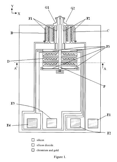
Figure 1 illustrates a gripper with integrated active release plunger;
Figure 2 is a cross-sectional view of the gripper corresponding to Figure 1
along axis
A-A;
Figure 3 illustrates an example of pick-place sequence using an embodiment of
the
present invention;
Figure 4 shows the experimental landing result of 10 m microspheres with the
use of
active release plunger, proving an accuracy better than 18% of micro object
size;
Figure 5 illustrates fabrication process A;
Figure 6 illustrates a general fabrication process;
7
CA 02750918 2011-07-27
WO 2010/094102 PCTICA2009/000181
Figure 7 illustrates fabrication process B;
Figure 8 shows an SEM image of the microgripper with active release plunger
fabricated
using Process (A);
Figure 9 shows an SEM. image of the gripper tip fabricated using Process (B).
The
labelled dimensions illustrate the difference in thickness between the gripper
tip vs. the
rest of the structure;
Figure 10 shows an alternative configuration of active release mechanism where
bimorph
microactuator is used.
In the drawings, one or more embodiments of the present invention are
illustrated by way
of example- It is to be expressly understood that the description and drawings
are only for
the purpose of illustration and as an aid for understanding, and are not
intended as a
definition of the limits of the present invention.
Detailed Description of the Invention
The present invention provides a device comprising an active release plunger
capable of
highly repeatable, accurate pick and place of micro and nanometer-sized
objects. In
particular, the present invention overcomes the drawbacks of existing designs
(i.e.,
release and down scaling) and provides a micro-nanomanipulation tool that can
grasp and
release objects on demand, and can be readily down scaled through a new
microfabrication process.
Thus, in one aspect the present invention is a device for manipulating
nanometer-scale
sized objects or micrometer-scale sized objects , characterized in that the
device
comprises:
(a) gripping arms for grasping the objects;
(b) a release plunger for actively releasing the objects from gripping arms;
and
(c) microactuation means connected to the gripping arms and the release
plunger and operable to actuate the gripping arms and said release plunger to
grasp
and actively release the objects from the gripping arms.
8
CA 02750918 2011-07-27
WO 20.10/094102 PCTICA20091000181
In another aspect, a novel microfabrication method is described, enabling the
patterning
of two layers of materials from a single side of a wafer. This
microfabrication method can
be integrated into most standard microfabrication processes that involve multi-
layered
wafers (e.g_, silicon-on-insulator wafer) in order to construct devices with
both
high-aspect-ratio structures and thin end structures. In the context of
devices for
micromanipulating nano-scale sized objects, this inicrofabrication method
permits the
construction of devices with both high-aspect-ratio structures and low aspect
ratio
structures with a thickness that is comparable to nanometer-sized objects to
be
manipulated. Thus, in yet another aspect, the present invention is a method of
manufacturing a device for manipulation of nano-scale sized objects comprising
high-aspect-ratio structures and low-aspect-ratio structures, characterized in
that said
method comprises:
(a) , providing a wafer having a top side and a bottom side, said wafer
comprising a top layer, a middle layer and a bottom layer, wherein said layers
are
made of materials having a suitable etch selectivity;
(b) patterning etching the top layer into a desired final pattern of the top
layer
corresponding to the device;
(c) applying onto the top layer a photoresist mask, and pattern said mask into
a desired final pattern of the middle layer corresponding to the high-aspect-
ratio
structures of the device;
(d) etching from the top side the exposed areas of the middle layer until the
bottom layer;
(e) etching from the top side the exposed areas of the top layer and the
bottom
layer;
(f) etching from the top side the exposed areas of the middle layer, thereby
forming the low-aspect-ratio structures of the device.
In yet another aspect, the present invention is a method for grasping and
placing an object
to a desired target area with the use of a device capable of manipulating
nanometer-scale
sized objects and micrometer-scale sized objects, said device comprising
gripping arms
9
CA 02750918 2011-07-27
WO 201.0l094102 PCx/CAzoo9/000lal
capable of opening and closing around the object, a release plunger for
actively releasing
the object from the gripping arms, and microactuation means connected to the
gripping
arms and the plunger and operable to actuate said gripping arms and release
plunger,
characterized in that said method comprises the following steps.
(a) closing the gripping arms around the object to grasp;
(b) moving the device to lift the object up and transport the object to the
desired target area;
(c) opening the gripping arms; and
(d) activating the plunger to actively release the object attached by adhesion
forces to an arm of the gripping arms thereby placing the object on the target
area
Manipulation in the context of this invention means to perform displacement
and
assembly tasks on nano-scale or micro-scale objects, including, without
limitation,
grasping, lifting, pushing, releasing and injecting nano-scale or micro-scale
objects.
Figures I and 2 illustrate one embodiment of the grasping and active releasing
device of
the present invention. In this embodiment the grasping and active releasing
device
comprises an electrostatically actuated microgipper comprising of three parts:
(i) two
electrostatic comb-drive microactuators B and C each controlling one of the
two gripping
arms 01 and G2 for grasping and gripper-plunger alignment; (ii) electrostatic
comb-drive
actuator L controlling active release plunger; and (iii) Linear beam flexures
Fl, F2 and
F3 used to transform actuated forces into displacements.
In the embodiments of Figures I and 2, the gripper and the plunger are
actuated by lateral
comb-drive microactuators. However, it should be understood that other types
of
electrostatic actuators, electrothermal actuators, or other types of
microactuators in
combination with motion/force amplification/reduction mechanisms are possible
and
within the scope of the present invention.
Lateral comb-drive microactuators are ideal for micro-nanomanipulation due to
its high
bandwidth, high motion resolution, no temperature gradient, ease to implement,
and
adequate force output to overcome surface adhesion forces. By changing the
dimensions
of the flexure Fl, F2 and F3 or the dimensions of comb-drive 13, C and D, the
motion
CA 02750918 2011-07-27
WO 2010/094102 PCT/CA2009/000181
range and resolution of the actuators can be adjusted.
Comb-drive microactuator B produces forces to deflect flexures El. The linear
motion is
directly transferred to the gripping arm G1. The second gripping arm G2
connected to
microactuator C through flexure F2 has a symmetrical configuration. The
gripping arms
are individually controlled by applying voltage between electrode E2 and El,
or E4 and
E I . The gripping tip separation determines the suitable size of the object
to be grasped.
The active release plunger P is controlled by applying a voltage between
electrode E3 and
El, where the forces produced by the comb-drive microactuator deflect flexures
F3 and
produce linear motions. The four tethered flexures F3 minimize out-of-plane
motion in
the x-y plane, relative to the plunger tip.
The active release plunger may be used in different ways. To achieve a
substrate
independent release, a sharp increase in the actuation voltage will allow the
plunger P to
move at a high speed and collide with the object adhered to one of the
gripping arms GI
or 02. The impact allows the adhered object to gain sufficient momentum to
overcome
the adhesion forces between the object and a gripping arm, resulting in
release. In the
case when the plunger moves at a relatively low speed, the adhered object can
be pushed
off from the gripping arm and directly into the substrate; however, the
success in release
depends on adhesion force differences between the plunger-object and the
object-substrate contact surfaces. When a plunger is extended beyond the
gripping arm
tip, it can also function as a needle probe for manipulation.
Different actuation voltage rising profiles result in different plunger speed
and force. One
particular experiments on 10 m sized microspheres demonstrated that a sharp
increase
in actuation voltage results in guarantee release. Quantification of maximum
plunging
speed using high-speed videography (13000 frames per second) reveals a
plunging speed
of 65.24mm/s produces a microsphere speed of 105.01mm/s. A high plunging speed
alleviates careful sample preparation requirements (e.g., baking) or
environmental control
requirements (e.g., humidity).
Figure 3 illustrates an example of micromanipulation sequence of microspheres
using a
high speed plunger, (a) the microgripper approaches a tnicrosphere and may use
one
gripping arm to laterally push it to break the initial adhesion bond between
the
11
CA 02750918 2011-07-27
WO 2010/094102 PCT/CA2009/000181
microsphere and the substrate. (b) Two gripping arms are closed, grasping the
microsphere and lifting it up. (c) The microsphere is transported to the
target area and
positioned a minimum distance above the substrate. (d) The gripping arms are
opened
and the gripping arm that the microsphere adheres to positions the microsphere
properly
to the right position in relation to the plunger. (e) The plunger thrusts out
the microsphere
that lands accurately on the substrate. (h) Microgripper retracts to repeat
the pick-place
process.
The landing accuracy is inversely proportional to the height of the gripping
arms and
plunger above the substrate. To achieve a high accuracy, the microgripper
should be
placed at a small distance above the destination. Using a high speed plunger,
the micro
object is separated from the plunger upon impact, hence the release capability
is
independent of the substrate. Note that the term substrate herein refers to
any surface for
object to be released on, including on top of another object such as during
the
construction of three-dimensional structures. Figure 4 shows representative
experimental
accuracy results for active release of 10 m microspheres from 2 m above the
substrate.
The release accuracy in this particular setup is 0.7 0.46 m.. Since the
positioning
system had a --1 M precision/repeatability and the environmental parameters
were not
strictly controlled, the release accuracy of the technique alone is expected
to be better
than a few hundreds of nanometers.
This intuitive active release design is the first-of-its-kind to allow a
micro-nanometer-sized object to be picked up and released in both ambient and
vacuum
environments. In aspects of this invention, the objects' size range from about
1 tun to
about 500 m. This new tool can find a range of applications. For example,
physical
modification and dissection a biology cell in electron microscopes for
cytology research,
and automated operation to construct three-dimensional novel micro-nano
structures
under optical and electron microscopes.
Two fabrication processes for forming the devices of the present invention are
illustrated
in Figure 5 and Figure 7. Figure 5 shows microfabrication process (A) for
devices
capable of micromanipulating objects down to -IM. Figure 7 shows a modified
fabrication process (B) for devices capable of nanoinanipulating sub-
micrometer and
12
CA 02750918 2011-07-27
WO 2010/094102 PC ICA2009/000181
nanometer-sized objects. Both processes use an SOl (silicon-on-insulator)
wafer.
Suitable SO) wafers for both microfabrication processes include SOI wafers
having a
200-500 m thick silicon handle layer, a O.l-2 m thick of a buried insulating
layer, such
as a SiO2 box layer, and a 10-300 m thick silicon device layer-
Steps for process (A) include:
I . Start with an SO) wafer 60.
2. Handle layer 20 of the wafer 60 is etched using, for example, DRIE (deep
reactive ion
etching) until the buried oxide layer 40(photolithographic mask 1).
3. Ohmic contacts 30 are formed by e-beam evaporation and patterned by lift-
off
(photolithographic mask 2).
4. Device layer 50 is patterned using photolithographic mask 3, and then
etched using
DRIE until the BOX (buried oxide) layer.
5. SiO2 BOX layer is etched and the individual devices 10 are released from
wafer 60.
To manipulate nanometer-sized objects, the gripping tip ideally should have a
comparable
thickness to the object. Based on standard SOI fabrication processes,
microgrippers
produced by process (A) can only be scaled down by reducing the thickness of
the whole
device, which induces problems such as undesired out-of plane motion resulting
from
poor aspect ratio in flexures, reduced microactuator performance; and reduced
device
structural integrity.
To overcome the problems associated with reducing the thickness of the whole
device, it
is ideal to selectively reduce only the thickness of the gripping tips while
maintaining the
thick structure for the rest of the device. This can be conceptually achieved
on a silicon
wafer with a thin oxide layer on top. The oxide layer forms the gripping tip
structure and
the silicon layer forms the rest of the device structures. However, a device
created in this
manner cannot be more than a couple of hundred micrometers thick, making it
difficult
to handle without device breakage. To overcome the device handling issue, an
SOl wafer
can be conveniently used to provide an additional handling layer for
structural support.
For a wafer with more than two material layers (e.g., an SOl wafer has three
layers
device silicon layer, buried oxide layer, and handle silicon layer), no
standard, existing
13
CA 02750918 2011-07-27
WO 2010/094102 PCTICA2009/000181
microfabrication processes are able to form different patterns on each layer.
The present
invention describes a novel general fabrication process that enables the
patterning of two
layers of materials from a single side of a wafer, as shown in figure 6 and
described
below. In the case of an SOl wafer, this new process allows the buried oxide
layer to be
patterned differently from the device silicon layer and be patterned to form
thin gripping
tips for manipulating sub-micrometer and nanometer sized objects. This new
process
allows wafers with up to four different material layers to be patterned
separately using
conventional micromachining processes.
Using a general example to describe the general process, a wafer with two
material layers,
layer A (top) and layer B (bottom), can both be patterned from a single side
of the wafer
through the following steps (Figure 7):
1. Deposit a layer of material B onto layer A as etch mask.
2. Pattern the deposited layer into final desired pattern of layer S.
3. Pattern a mask photoresist on deposited layer B into final desired pattern
of layer A.
4, Etch exposed material A from top.
5. Etch exposed material B from top.
6. Etch exposed material A from top.
The working conditions for process (X) include:
1. Suitable etching methods are available for etching materials A and B.
2. Materials A and B have suitable etch selectivity, such as between Silicon
and Si02
3. Pbotoresist can withstand etching of both material A and B.
By integrating this novel fabrication process (X) into process (A), where
material A is the
device silicon layer and material H is the BOX layer of an SOT wafer, the new
microfabrication process (B) includes the following steps:
I . A material 110 having a preselected electrical resistivity, such as Si02,
is thermally
grown on both sides of an SOl wafer 160.
2. Chromium is evaporated onto device layer 150, and patterned to define
features such
14
CA 02750918 2011-07-27
WO 2010/0941.02 PCT/CA2009/000181
as comb fingers and flexures (photolithographic mask 1).
3. Top SiO2 layer is etched with R1E (reactive ion etching) using
photolithographic
mask 2 and predefined Cr etch mask-
4. Ohmic contacts 130 are formed by e-bearn evaporation and patterned by lift-
off
(mask 3).
5. Bottom SiO2 layer is patterned to form DRIE (deep reactive ion etching)
etch mask
on handle layer. ((rusk 4)
6. Handle layer 120 is etched using DRIE until SiO2 BOX layer.
7. A thin film of a material having a predetermined electrical conductivity
(metal/non-metal) is evaporated onto the handle layer.
8. Device layer 150 is patterned using photolithographic mask 5. Then the
exposed
silicon is etched using DRIE.
9. Exposed SiO2 from both top layer and BOX layer are etched from the top.
10. Exposed metal/non-metal thin film is etched using RIB from the top.
11. Exposed device layer silicon is etched using DRIE from the top.
12. (optional depending on needs) Exposed SiO2 from top layer and BOX layer
are
etched away from the top to expose metal/non-metal thin film at gripping tip.
The general process illustrated in Figure 7 is integrated into process (B) as
steps 1, 3, 8, 9,
and 11, permitting the device silicon layer to be patterned into device
structures
(microactuators and flexures), and the BOX layer to be patterned into gripping
tips.
Through the integration of the general process with process (A), it is now
possible to
selectively reduce the gripping tip thickness to sub-micrometers for
manipulating
nanometre sized objects.
Due to the increased complexity in fabrication sequence, step 2 in process (B)
was added
to minimize alignment issues with small features.
Depending on the application requirement, process B allows the gripping tip to
be made
from a broad range of materials, conductive or non-conductive (determined by
Process B,
CA 02750918 2011-07-27
WO 20,101094102 PCT/CA2009/000181
step 7). When the gripping is used upside down inside an SEM (scanning
electron
microscope), the deposited thin film (Process B, step 7) can also prevent
charging effect
and provide clearer images. The working environment for this type of grippers
includes
ambient and vacuum environments.
Figure 8 shows an SEM image of an example gripper with a plunger for active
release
fabricated using Process (A). The device is suitable for micromanipulation of
objects
down to about I m in size. Figure 9 shows an SEM image of an example gripper
with a
plunger for active release fabricated using Process (B). The device is
suitable for
nanomanipulation of objects smaller than about 1 m in size.
It should be understood that the present invention is the first-of-its-kind in
terms of active
release repeatability and accuracy. The present invention is also the first-of-
its-kind to
allow precise thickness control over the microgripper tip without changing the
thickness
of device layer, through theintegration of a novel fabrication process (X)
into fabrication
process (A).
The above descriptions relate to active release through in-plane motions of a
plunger. An
alternative configuration for active release is to replace the microactuator D
in Figure 1
with an out-of-plane microactuator. For example, the plunger can be replaced
by a
thermal bimorph microactuator, as shown in Figure 9. The top layer 310
comprises a
deposited material with higher thermal expansion coefficient than the bottom
layer. When
heat is generated, the difference in thermal coefficients will drive the tip
of the plunger in
the direction indicated by the arrow (negative Z direction), releasing an
adhered object
through the out-of-plane motion from the plunger.
It will be appreciated by those skilled in the art that other variations of
the one or more
embodiments described herein are possible and may be practiced without
departing from
the scope of the present invention.
16
CA 02750918 2011-07-27
WO 2010/094102 PCT/CA2009/000181.
1. A device for manipulating manometer-scale sized objects or micrometer-scale
sized
objects, characterized in that the device comprises:
(a) gripping arms for grasping the objects;
(b) a release plunger for actively releasing the objects from gripping arms;
and
(c) microactuation means connected to the gripping arms and the release
plunger and
operable to actuate the gripping arms and said release plunger to grasp and
actively
release the objects from the gripping arms.
2. The device of claim 1, characterized in that said microactuators include
electrostatic
microactuators, electrothermal microactuators or piezoelectric actuators.
3. The device of claim 1 further characterized in that the device is operable
to grasp and
actively release objects ranging in size from about I ran to about 500 urn.
4. The device of claim 1, characterized in that the plunger is operable to
impact the objects
with a releasing force greater than an adhesion force acting between the
objects and an
arm of the gripping arms thereby actively releasing the objects from the
gripping arms.
5. The device of claim 1, characterized in that the plunger is operable to
push off the objects
attached to an arm of the gripping arms by adhesion forces thereby actively
releasing the
objects from the gripping arms.
6. The device of claim 1, characterized in that the release plunger is
operable to produce
variable plunging speeds and forces.
7. The device of claim 1, characterized in that said microactuation means
comprise a first
set of microactuators connected to the gripping arms and a second set of
microactuators
connected to the release plunger, thereby allowing flexible manipulation and
alignment
between the gripping arms and the plunger.
17
CA 02750918 2011-07-27
WO 20101094102 PCB'/CA2009/000181
8. The device of claim 7, characterized in that the second set of
microactuators comprise in-
plane microactuators that permit the plunger to impact the object from an in-
plane
direction; or the second set of microactuators comprise out-of-plane
microaetuators that
permit the plunger to impact the object from an out-of-plane direction.
9. The device of claim 7, characterized in that the first set of
microactuators comprise
microactuators independently connected to each arm of the gripping arms.
10. The device of claim 1, characterized in that the gripping arms and the
plunger are
connected to the microactuation means by flexures,
11. The device of claim 1 further characterized in that said plunger further
functions as a
probe for manipulation of the objects.
12. The device of claim 1, characterized in that the gripping arms are
operable between a
close position and an open position to grasp objects and allow for the release
of said
objects, and said plunger is operable to actively release the objects attached
by adhesion
forces to an arm of the gripping arms while said arms are in the open
position.
13. A method of manufacturing a device for manipulating nanometer-scale sized
objects or
micrometer-scaled sized objects, said device comprising structural elements,
said
structural elements including gripping arms for grasping the objects, a
release plunger for
actively releasing the objects from gripping arms, and microactuatoon means
connected to
the gripping arms and the release plunger and operable to actuate the gripping
arms and
said release plunger to grasp and actively release the objects from the
gripping arms,
characterized in that said method comprises the following steps:
(a) providing a wafer having a top side and a bottom side, said wafer
comprising a
top layer, a middle layer and a bottom layer, wherein said layers are made of
materials having a suitable etch selectivity;
(b) patterning etching the top layer into a desired final pattern of the top
layer
corresponding to the device;
18
CA 02750918 2011-07-27
WO 2010/094102 Pe /CA2009/000181
(c) etching from the top side exposed areas of the middle layer until the
bottom layer;
and
(d) etching from the top side exposed areas of the bottom layer,
thereby providing the device for micromanipulating objects.
14. The methods of claims 13, wherein the gripping arms comprise gripping tips
having a
thickness, characterized in that said method is capable of selectively
reducing the
thickness of said tips with respect to the structural elements, said method
comprising after
step (b):
(c) applying onto the top layer a photoresist mask, and pattern said mask into
a
desired final pattern of the middle layer corresponding to the structural
elements
of the device;
(d) etching from the top side exposed areas of the middle layer until the
bottom layer,
(e) etching from the top side exposed areas of the top layer and the bottom
layer; and
(f) etching from the top side exposed areas of the middle layer, thereby
providing the
device comprising gripping tips having their thickness reduced with respect to
the
structural Elements.
15. The method of claim 13, characterized in that said wafer is a silicon-on-
insulator wafer,
wherein said middle layer is a device silicon layer and said bottom layer is a
buried
insulating layer between said device layer and a handle silicon layer, and
wherein prior to
step (b) the method further comprises applying to the Dandle silicon layer a
bottom layer
of a material having a suitable etch selectivity, and patterning etching the
bottom layer
from the bottom side into a desired final pattern of the handle layer until
the buried
insulating layer.
16. The method of claim 15, characterized in that said method further
comprises applying
from the bottom side a film of a material having a predetermined electrical
conductivity.
19
CA 02750918 2011-07-27
WO 2010/094102 PCTICA2009/000181
17_ The method of claim 16, wherein the gripping arms comprise gripping tips
having a
thickness, characterized in that said method is capable of selectively
reducing the
thickness of said tips with respect to the structural elements of the device,
said method
comprising after step (b):
(c) applying onto the top layer a photoresist mask, and pattern said mask into
a
desired final pattern of the device silicon layer corresponding to the
structural
elements of the device;
(d) etching from the top side exposed areas of the device silicon layer until
the buried
insulating layer,
(e) etching from the top side exposed areas of the top layer and the buried
insulating
layer;
(f) etching from the top side exposed areas of the device silicon layer; and
(g) etching from the top side exposed areas of the buried silicon layer until
the film
material having a predetermined electrical conductivity, thereby providing the
device comprising gripping tips having their thickness reduced with respect to
the
structural elements.
18. The methods of claims 13 to 17, characterized in that said patterning
steps are performed
by means of photolithography masks.
19. The methods of claims 13 to 15, characterized in that the top layer and
the bottom layer
are silicon dioxide layers.
20. The methods of claims 13 to 14, characterized in that said middle layer is
a silicon layer.
21. The methods of claims 16 to 17, characterized in that said material having
the
predetermined electrical conductivity is electrically conductive,
22. The methods of claims 16 to 17, characterized in that said material having
the
predetermined electrical conductivity is electrically non-conductive.
CA 02750918 2011-07-27
WO 2010/094102 PCT/C,A,2009/000181
23. The methods of claims 13 to 17, characterized in that said methods further
comprise
forming ohmic contacts.
24. The methods of claims 14 and 17, characterized in that said device is
capable of grasping
and actively releasing objects smaller than about I micrometer in size.
25. The methods of claims 14 and 17, characterized in that said thickness of
the gripping tips
is reduced to a level comparable to the objects to be grasped and released.
26. A method of manufacturing a device for manipulating manometer-scale sized
objects or
micrometer-scale sized objects, said device comprising structural elements,
said
structural elements including gripping arms for grasping the objects, a
release plunger for
actively releasing the objects from gripping arms, and microactuation means
connected to
the gripping arms and the release plunger and operable to actuate the gripping
arms and
said release plunger to grasp and actively release the objects from the
gripping arms,
characterized in that said method comprises patterning etching a silicon-on-
insulator
wafer from a single side of said wafer.
27. A method of manufacturing a device for manipulating nanometer-scale sized
objects or
micrometer-scale sized objects, said device comprising high-aspect-ratio
structures and
low-aspect-ratio structures, characterized in that said method comprises;
(a) providing a wafer having a top side and a bottom side, said wafer
comprising a
top layer, a middle layer and a bottom layer, wherein said layers are made of
materials having a suitable etch selectivity;
(b) patterning etching the top layer into a desired final pattern of the top
layer
corresponding to the device;
(c) applying onto the top layer a photoresist mask, and pattern said mask into
a
desired final pattern of the middle layer corresponding to the high-aspect-
ratio
structures of the device;
(d) etching from the top side the exposed areas of the middle layer until the
bottom
layer;
21
CA 02750918 2011-07-27
WO 2010/094102 PCT/CA2009/000181
(e) etching from the top side the exposed areas of the top layer and the
bottom layer;
(f) etching from the top side the exposed areas of the middle layer, thereby
forming
the low-aspect-ratio structures of the device.
28. The method of claim 28, characterized in that said high-aspect-ratio
structures include
gripping arms for grasping the objects; a release plunger for actively
releasing the objects
from gripping arms; and microactuation means connected to the gripping arms
and the
release plunger and operable to actuate the gripping arms and said release
plunger to
grasp and actively release the objects from the gripping arms, and wherein
said low-
aspect-ratio end structure include gripping tips of said gripping arms.
29. The method of claim 28, characterized in that said objects are nanometer-
scale sized
objects.
30. A method for grasping and placing an object to a desired target area with
the use of a
device capable of manipulating nanometer-scale sized objects or micrometer-
scale sized
objects, said device comprising gripping arms capable of opening and closing
around the
object, a release plunger for actively releasing the object from the gripping
arms, and
microactuation means connected to the gripping arms and the plunger and
operable to
actuate said gripping arms and release plunger, characterized in that said
method
comprises the following steps:
(a) closing the gripping arms around the object to grasp;
(b) moving the device to lift the object up and transport the object to the
desired
target area;
(c) opening the gripping arms; and
(d) activating the plunger to actively release the object attached by adhesion
forces to
an arm of the gripping arms thereby placing the object on the target area.
22
CA 02750918 2011-07-27
WO 2010/094102 PCT/CA20091000181
31. The method for grasping and placing an object to a desired target area of
claim 30,
characterized in that said microactuation means are independently connected to
the
gripping arms and to the release plunger thereby allowing flexible alignment
between the
gripping arm to which the object is attached and the plunger.
23