Note: Descriptions are shown in the official language in which they were submitted.
CA 02751456 2012-08-22
Method and Product for Cutting Materials
Field
[0002] The present disclosure relates to a method for cutting
materials, wherein the
method includes using wires formed from relatively ductile iron based glass
forming
material.
Background
[0003] Existing wires utilized for wire saws may typically be made of
relatively high
tensile steel which may be deep drawn down to achieve relatively fine wire
diameters in the
range of 140 to 380 pm. The lower limit in wire diameter may be limited by the
number and
practicality of stages of conventional wire drawing, and the ability to
achieve significant
levels of ductility which are reduced from work hardening. Wire cutting saws
may include
two different varieties, such as slurry abrasive or diamond wire saws. In
slurry abrasive wire
cutting, a bare steel wire or brass coated steel wire may be utilized in
combination with a
slurry abrasive which may include a relatively large variety of abrasives such
as SiC. The
relatively fast moving wire may contact the abrasive in the liquid slurry,
which may become
trapped between the wire and the substrate resulting in the cutting of the
substrate. In
diamond wire cutting, a steel wire may be used as the wire base, which is then
coated with an
electrolytic copper sheet impregnated with diamonds, and 10 to 120 pm in size.
The entire
wire may then be coated with a nickel overstrike to reinforce the wire. As may
be
appreciated the steel base wire is one factor limiting the total wire diameter
and the
impregnated copper and nickel coatings add to the diameter. 'Ibere may be
several
advantages and disadvantages between the slurry abrasive wire and diamond wire
cutting
techniques. For wafer cutting, a diamond coated wire can offer advantages such
as the
precision of the cut compared to slurry abrasion cutting which may wander.
Alternately,
slurry abrasive cutting offers an advantage with respect to lower edge
chipping compared to
1
CA 02751456 2011-08-03
WO 2010/091087
PCT/US2010/023054
diamond wire cutting and, accordingly, slurry abrasive wire cutting appears to
be used
prevalently in cutting large diameter silicon ingots.
[0004] For
any high value material including silicon, germanium, gallium arsenide,
quartz, glass, etc., the material losses or kerf losses during cutting may be
significant. One
overriding factor in total kerf loss during cutting may be the wire diameter
utilized, wherein
smaller wire diameters may lead to lower kerf losses. The following case
example regarding
silicon wafer illustrates the value of these losses for silicon in the
microelectronics and
photovoltaic industries.
[0005]
That is, one key cost factor for silicon wafer processing may include the
material lost during cutting or kerf losses. As the price of raw materials has
increased and the
thickness of the wafer has decreased, the kerf loss has been an increasingly
important factor.
With current wire technology it has been estimated that the kerf thickness
loss may ultimately
be brought down to 150 p m in thickness. Furthermore, this loss becomes
increasingly
important as wafer size decreases. For example, for industrial solar cells, in
2004 the average
thickness was 330 p m but by 2007, the average wafer thickness was 210 p m.
Additionally,
the recycling of silicon kerf is challenging since it is exists in a slurry
with polyethylene
glycol liquid containing impurities including iron from the wire and SiC
abrasives.
[0006] In
2006, the world wide production capacity of polysilicon was at 37,500 tons.
It has been estimated that 70% of all polysilicon feedstock ends up as usable
silicon ingot
resulting in 26,250 tons produced. The average kerf loss in wafer sawing
process is
estimated to be 35% which results in a total silicon waste at 9,188 tons. In
2006, the average
price per pound of silicon varied widely depending on the type with the
following values
published; Solar Poly Price at $36.3/1b, Semiconductor CZ Price at $27.21/1b,
Semiconductor
FZ Price at $90.70/1b and Spot Market Price depending on availability at
$136.05/1b. A
conservative estimate based on prices above is a cost basis of $55/1b for
value of
microelectronic grade silicon. Thus, the yearly monetary value of kerf waste
can be
estimated at $1.01 Billion dollars per year. Furthermore, manufacturing of
microelectronic
grade silicon is relatively energy intensive and involves high temperatures at
extended times
in order to extract, purify, and grow crystals from the melt. It has been
estimated that
electron energy usage is 90.7 MW hours per ton of silicon ingot. The average
kerf loss in the
wafer sawing process as stated earlier is 9,188 tons. Thus, the total energy
lost for wasted
2
CA 02751456 2011-08-03
WO 2010/091087
PCT/US2010/023054
silicon is 833,352 MW hours. Considering a rough estimate of the average cost
of electricity
at $10.00 per MW hour, then the total wasted electricity cost is $0.83 billion
dollars per year.
Summary
[0007] An aspect of the present disclosure relates to a wire, which may
include an
iron based glass forming alloy. The alloy may include iron present in the
range of 43.0 to
68.0 atomic percent, boron present in the range of 12.0 to 19.0 atomic
percent, nickel present
in the range of 15.0 to 17.0 atomic percent, cobalt present in the range of
2.0 to 21.0 atomic
percent, optionally carbon present in the range of 0.1 to 6.0 atomic percent
and optionally
silicon present in the range of 0.4 to 4.0 atomic percent. The wire may have a
thickness of
140 p m or less and include spinodal glass matrix microconstituents.
[0008]
Another aspect of the present disclosure relates to a method of cutting
substrates. The method may include abrading a substrate with a wire including
an iron based
glass forming alloy. The alloy may include iron present in the range of 43.0
to 68.0 atomic
percent, boron present in the range of 12.0 to 19.0 atomic percent, nickel
present in the range
of 15.0 to 17.0 atomic percent, cobalt present in the range of 2.0 to 21.0
atomic percent,
optionally carbon present in the range of 0.1 to 6.0 atomic percent and
optionally silicon
present in the range of 0.4 to 4.0 atomic percent. The wire may have a
thickness of 140 p m or
less and include spinodal glass matrix microconstituents.
[0009] A further aspect of the present disclosure relates to a method of
forming a
wire. The method may include melting elemental constituents to provide an iron
based glass
forming alloy and forming the iron based glass forming alloy into a wire
exhibiting a
thickness of 140 p m or less wherein the wire includes spinodal glass matrix
microconstituents. The alloy may include iron present in the range of 43.0 to
68.0 atomic
percent, boron present in the range of 12.0 to 19.0 atomic percent, nickel
present in the range
of 15.0 to 17.0 atomic percent, cobalt present in the range of 2.0 to 21.0
atomic percent,
optionally carbon present in the range of 0.1 to 6.0 atomic percent and
optionally silicon
present in the range of 0.4 to 4.0 atomic percent
3
CA 02751456 2011-08-03
WO 2010/091087
PCT/US2010/023054
Brief Description of the Drawings
[0010] The
above-mentioned and other features of this disclosure, and the manner of
attaining them, may become more apparent and better understood by reference to
the
following description of embodiments described herein taken in conjunction
with the
accompanying drawings, wherein:
Figure 1 illustrates an example schematic of a wire saw.
Figure 2 illustrates an example long length of flat wire (ribbon) which was
produced
at 10.5 m/s.
Figure 3 illustrates an example spool which is shown of glass coated microwire
of
Run #6.
Figure 4 illustrates an example of a DTA analysis of the PC7E10S2A1 alloy when
produced as a glass coated circular wire; top curve with water cooling, bottom
curve, without
water cooling.
Figure 5 illustrates an example of a DTA analysis of the PC7E10S1B2 alloy when
produced as a glass coated circular wire; top curve without water cooling,
bottom curve, with
water cooling.
Figure 6 illustrates an example of a DTA analysis of the PC7E10S2A1 alloy; top
curve flat wire bottom curve, glass coated circular wire.
Figure 7 illustrates an example of a DTA analysis of the PC7E10S1B2 alloy; top
curve flat wire, bottom curve, glass coated circular wire.
Figure 8 illustrates an example of an SEM BSE image of the Spool # 6 microwire
showing the wire with the glass coating.
Figure 9 illustrates an example of an SEM BSE image of the Spool #6 microwire
showing the wire with the glass coating and with the coating removed near the
tip showing
the bare wire.
Figure 10 illustrates an example of an SEM BSE image of the Spool #6 microwire
showing a close-up of the wire structure with the glass coating removed.
Figure 11 illustrates an example of an SEM image of the microwire rope from
Spool
#6 which was used for tensile testing.
Figure 12 illustrates an example of an SEM BSE image of a microwire from Spool
#6
which was twisted under tension to produce both tensile and torsional strains.
4
CA 02751456 2011-08-03
WO 2010/091087
PCT/US2010/023054
Figure 13 illustrates an example of two TEM images of a microwire from Spool
#6.
Note that in the corner of each micrograph, selected area diffraction patterns
are shown.
Detailed Description
[0011] The present disclosure relates to a composition, method and process
for using
wires formed of an iron based glass forming alloy. Such wires may be
relatively finer in size,
which may result in relatively lower kerf cutting waste. The glass based
forming alloy may be
understood as an iron alloy wherein the alloy may be relatively amorphous, or
may exhibit
micro- or nano-structures, which may be understood as associations of
structural units in the
solid phase that may be randomly packed together. In some examples, the micro-
or nano-
structures may be present in ranges of 1 to 100% by volume in the alloy
composition,
including all values and increments therein. In other examples, the glass may
be presented in
ranges of 1 to 90 % by volume of the alloy composition, including all values
and increments
therein. Relatively amorphous alloys or alloy fractions may exhibit little to
no ordering on the
atomic level. The micro- or nano-structures may be in the range of 0.1 nm to
1.0 micron in
size, including all values and increments therein.
[0012]
Furthermore, the alloys may form Spinodal Glass Matrix Microconstituent
(SGMM) structures that may exhibit relatively significant ductility and
relatively high tensile
strength. Spinodal microconstituents may be understood as microconstituents
formed by a
transformation mechanism which is not nucleation controlled. More basically,
spinodal
decomposition may be understood as a mechanism by which a solution of two or
more
components (e.g. metal compositions) of the alloy can separate into distinct
regions (or
phases) with distinctly different chemical compositions and physical
properties. This
mechanism differs from classical nucleation in that phase separation occurs
uniformly
throughout the material and not just at discrete nucleation sites. One or more
semicrystalline
clusters or crystalline phases may therefore form through a successive
diffusion of atoms on a
local level until the chemistry fluctuations lead to at least one distinct
crystalline phase.
Semi-crystalline clusters may be understood herein as exhibiting a largest
linear dimension of
2 nm or less, whereas crystalline clusters may exhibit a largest linear
dimension of greater
than 2nm. Note that during the early stages of the spinodal decomposition, the
clusters which
are formed may be relatively small and while their chemistry differs from the
glass matrix,
5
CA 02751456 2011-08-03
WO 2010/091087
PCT/US2010/023054
they are not yet fully crystalline and have not yet achieved well ordered
crystalline
periodicity. Additional crystalline phases may exhibit the same crystal
structure or distinct
structures. Furthermore the glass matrix may be understood to include
microstructures that
may exhibit associations of structural units in the solid phase that may be
randomly packed
together. The level of refinement, or the size, of the structural units may be
in the angstrom
scale range (i.e. 5A to 100 A).
[0013]
Accordingly, the present disclosure relates to a cutting methodology to cut
relatively high value materials including but not limited to silicon,
germanium, gallium
arsenide, quartz, glass, etc., into ingots, crystals, wafers, thin slices,
etc., which may result in
relatively lower cutting loss, thus improving material utilization and
reducing manufacturing
costs. In this approach, relatively thin microwires from 1 p m to 140 p m in
thickness (i.e.,
diameter) may be manufactured in a process that may form wires directly from a
liquid melt.
It is contemplated that wire production may be accomplished by utilizing a
casting process or
the Taylor-Ulitovsky wire making process in combination with relatively
ductile iron based
glass forming alloy chemistries to thereby produce wires that may exhibit
combinations of
relatively high tensile strength of greater than or equal to 1 GPa and tensile
elongation of
greater than or equal to 1.5%.
[0014] The
wires produced are contemplated to have a length of up to 1000
kilometers. More specifically, the wires may have lengths in the range of 500
meters or
greater, including all values and increments therein. For example, the wires
may have length
between 1 kilometer to 500 kilometers, including all values and increments
therein, in 0.5
kilometer variations. The wires may then be utilized in single or multi-wire
sawing, where a
workpiece to be sliced may be pushed into the wire web, which may be wound
from one side
to the other. For example, silicon pillars having a length of up to and
including 1 meter, after
treatment with the multi-wire sawing device, may be sliced into thousands of
wafers in a
single run. However, the present invention contemplates the use of the wires
on their own, for
slicing, and is not limited to use in such multi-wire sawing configurations.
[0015] The
alloy may include, consist essentially of or consist of in the range of 43.0
at.% (atomic percent) to 68.0 at.% iron, 12.0 at.% to 19.0 at.% boron, 15.0
at.% to 17.0 at.%
nickel and 2.0 at.% to 21.0 at.% cobalt, including all increments and values
within the given
ranges. The alloy may also, optionally, include carbon present in the range of
0.1 at. % to 6.0
at. % and silicon present in the range of 0.4 to 4.0 atomic percent, including
all increments
6
CA 02751456 2011-08-03
WO 2010/091087
PCT/US2010/023054
and values within the given ranges. Accordingly, it may be appreciated that
iron may be
present at values of 43.0 at. %, 43.1 at. %, 43.2 at. %, 43.3 at. %, 43.4 at.
%, 43.5 at. %, 43.6
at. %, 43.7 at. %, 43.8 at. %, 43.9 at. %, 44.0 at. %, 44.1 at. %, 44.2 at. %,
44.3 at. %, 44.4 at.
%, 44.5 at. %, 44.6 at. %, 44.7 at. %, 44.8 at. %, 44.9 at. %, 45.0 at. %,
45.1 at. %, 45.2 at. %,
45.3 at. %, 45.4 at. %, 45.5 at. %, 45.6 at. %, 45.7 at. %, 45.8 at. %, 45.9
at. %, 46.0 at. %,
46.1 at. %, 46.2 at. %, 46.3 at. %, 46.4 at. %, 46.5 at. %, 46.6 at. %, 46.7
at. %, 46.8 at. %,
46.9 at. %, 47.0 at. %, 47.1 at. %, 47.2 at. %, 47.3 at. %, 47.4 at. %, 47.5
at. %, 47.6 at. %,
47.7 at. %, 47.8 at. %, 47.9 at. %, 48.0 at. %, 48.1 at. %, 48.2 at. %, 48.3
at. %, 48.4 at. %,
48.5 at. %, 48.6 at. %, 48.7 at. %, 48.8 at. %, 48.9 at. %, 49.0 at. %, 49.1
at. %, 49.2 at. %,
49.3 at. %, 49.4 at. %, 49.5 at. %, 49.6 at. %, 49.7 at. %, 49.8 at. %, 49.9
at. %, 50.0 at. %,
50.1 at. %, 50.2 at. %, 50.3 at. %, 50.4 at. %, 50.5 at. %, 50.6 at. %, 50.7
at. %, 50.8 at. %,
50.9 at. %, 51.0 at. %, 51.1 at. %, 51.2 at. %, 51.3 at. %, 51.4 at. %, 51.5
at. %, 51.6 at. %,
51.7 at. %, 51.8 at. %, 51.9 at. %, 52.0 at. %, 52.1 at. %, 52.2 at. %, 52.3
at. %, 52.4 at. %,
52.5 at. %, 52.6 at. %, 52.7 at. %, 52.8 at. %, 52.9 at. %, 53.0 at. %, 53.1
at. %, 53.2 at. %,
53.3 at. %, 53.4 at. %, 53.5 at. %, 53.6 at. %, 53.7 at. %, 53.8 at. %, 53.9
at. %, 54.0 at. %,
54.1 at. %, 54.2 at. %, 54.3 at. %, 54.4 at. %, 54.5 at. %, 54.6 at. %, 54.7
at. %, 54.8 at. %,
54.9 at. %, 55.0 at. %, 55.1 at. %, 55.2 at. %, 55.3 at. %, 55.4 at. %, 55.5
at. %, 55.6 at. %,
55.7 at. %, 55.8 at. %, 55.9 at. %, 56.0 at. %, 56.1 at. %, 56.2 at. %, 56.3
at. %, 56.4 at. %,
56.5 at. %, 56.6 at. %, 56.7 at. %, 56.8 at. %, 56.9 at. %, 57.0 at. %, 57.1
at. %, 57.2 at. %,
57.3 at. %, 57.4 at. %, 57.5 at. %, 57.6 at. %, 57.7 at. %, 57.8 at. %, 57.9
at. %, 58.0 at. %,
58.1 at. %, 58.2 at. %, 58.3 at. %, 58.4 at. %, 58.5 at. %, 58.6 at. %, 58.7
at. %, 58.8 at. %,
58.9 at. %, 59.0 at. %, 59.1 at. %, 59.2 at. %, 59.3 at. %, 59.4 at. %, 59.5
at. %, 59.6 at. %,
59.7 at. %, 59.8 at. %, 59.9 at. %, 60.0 at. %, 60.1 at. %, 60.2 at. %, 60.3
at. %, 60.4 at. %,
60.5 at. %, 60.6 at. %, 60.7 at. %, 60.8 at. %, 60.9 at. %, 61.0 at. %, 61.1
at. %, 61.2 at. %,
61.3 at. %, 61.4 at. %, 61.5 at. %, 61.6 at. %, 61.7 at. %, 61.8 at. %, 61.9
at. %, 62.0 at. %,
62.1 at. %, 62.2 at. %, 62.3 at. %, 62.4 at. %, 62.5 at. %, 62.6 at. %, 62.7
at. %, 62.8 at. %,
62.9 at. %, 63.0 at. %, 63.1 at. %, 63.2 at. %, 63.3 at. %, 63.4 at. %, 63.5
at. %, 63.6 at. %,
63.7 at. %, 63.8 at. %, 63.9 at. %, 64.0 at. %, 64.1 at. %, 64.2 at. %, 64.3
at. %, 64.4 at. %,
64.5 at. %, 64.6 at. %, 64.7 at. %, 64.8 at. %, 64.9 at. %, 65.0 at. %, 65.1
at. %, 65.2 at. %,
65.3 at. %, 65.4 at. %, 65.5 at. %, 65.6 at. %, 65.7 at. %, 65.8 at. %, 65.9
at. %, 66.0 at. %,
66.1 at. %, 66.2 at. %, 66.3 at. %, 66.4 at. %, 66.5 at. %, 66.6 at. %, 66.7
at. %, 66.8 at. %,
66.9 at. %, 67.0 at. %, 67.1 at. %, 67.2 at. %, 67.3 at. %, 67.4 at. %, 67.5
at. %, 67.6 at. %,
7
CA 02751456 2011-08-03
WO 2010/091087
PCT/US2010/023054
67.7 at. %, 67.8 at. %, 67.9 at. %, 68.0 at. %. Boron may be present at 12.0
at. %, 12.1 at. %,
12.2 at. %, 12.3 at. %, 12.4 at. %, 12.5 at. %, 12.6 at. %, 12.7 at. %, 12.8
at. %, 12.9 at. %,
13.0 at. %, 13.1 at. %, 13.2 at. %, 13.3 at. %, 13.4 at. %, 13.5 at. %, 13.6
at. %, 13.7 at. %,
13.8 at. %, 13.9 at. %, 14.0 at. %, 14.1 at. %, 14.2 at. %, 14.3 at. %, 14.4
at. %, 14.5 at. %,
14.6 at. %, 14.7 at. %, 14.8 at. %, 14.9 at. %, 15.0 at. %, 15.1 at. %, 15.2
at. %, 15.3 at. %,
15.4 at. %, 15.5 at. %, 15.6 at. %, 15.7 at. %, 15.8 at. %, 15.9 at. %, 16.0
at. %, 16.1 at. %,
16.2 at. %, 16.3 at. %, 16.4 at. %, 16.5 at. %, 16.6 at. %, 16.7 at. %, 16.8
at. %, 16.9 at. %,
17.0 at. %, 17.1 at. %, 17.2 at. %, 17.3 at. %, 17.4 at. %, 17.5 at. %, 17.6
at. %, 17.7 at. %,
17.8 at. %, 17.9 at. %, 18.0 at. %, 18.1 at. %, 18.2 at. %, 18.3 at. %, 18.4
at. %, 18.5 at. %,
18.6 at. %, 18.7 at. %, 18.8 at. %, 18.9 at. %, 19.0 at. %. Nickel may be
present at 15.0 at. %,
15.1 at. %, 15.2 at. %, 15.3 at. %, 15.4 at. %, 15.5 at. %, 15.6 at. %, 15.7
at. %, 15.8 at. %,
15.9 at. %, 16.0 at. %, 16.1 at. %, 16.2 at. %, 16.3 at. %, 16.4 at. %, 16.5
at. %, 16.6 at. %,
16.7 at. %, 16.8 at. %, 16.9 at. %, 17.0 at. %. Cobalt may be present at 2.0
at. %, 2.1 at. %,
2.2 at. %, 2.3 at. %, 2.4 at. %, 2.5 at. %, 2.6 at. %, 2.7 at. %, 2.8 at. %,
2.9 at. %, 3.0 at. %,
3.1 at. %, 3.2 at. %, 3.3 at. %, 3.4 at. %, 3.5 at. %, 3.6 at. %, 3.7 at. %,
3.8 at. %, 3.9 at. %,
4.0 at. %, 4.1 at. %, 4.2 at. %, 4.3 at. %, 4.4 at. %, 4.5 at. %, 4.6 at. %,
4.7 at. %, 4.8 at. %,
4.9 at. %, 5.0 at. %, 5.1 at. %, 5.2 at. %, 5.3 at. %, 5.4 at. %, 5.5 at. %,
5.6 at. %, 5.7 at. %,
5.8 at. %, 5.9 at. %, 6.0 at. %, 6.1 at. %, 6.2 at. %, 6.3 at. %, 6.4 at. %,
6.5 at. %, 6.6 at. %,
6.7 at. %, 6.8 at. %, 6.9 at. %, 7.0 at. %, 7.1 at. %, 7.2 at. %, 7.3 at. %,
7.4 at. %, 7.5 at. %,
7.6 at. %, 7.7 at. %, 7.8 at. %, 7.9 at. %, 8.0 at. %, 8.1 at. %, 8.2 at. %,
8.3 at. %, 8.4 at. %,
8.5 at. %, 8.6 at. %, 8.7 at. %, 8.8 at. %, 8.9 at. %, 9.0 at. %, 9.1 at. %,
9.2 at. %, 9.3 at. %,
9.4 at. %, 9.5 at. %, 9.6 at. %, 9.7 at. %, 9.8 at. %, 9.9 at. %, 10.0 at. %,
10.1 at. %, 10.2 at.
%, 10.3 at. %, 10.4 at. %, 10.5 at. %, 10.6 at. %, 10.7 at. %, 10.8 at. %,
10.9 at. %, 11.0 at. %,
11.1 at. %, 11.2 at. %, 11.3 at. %, 11.4 at. %, 11.5 at. %, 11.6 at. %, 11.7
at. %, 11.8 at. %,
11.9 at. %, 12.0 at. %, 12.1 at. %, 12.2 at. %, 12.3 at. %, 12.4 at. %, 12.5
at. %, 12.6 at. %,
12.7 at. %, 12.8 at. %, 12.9 at. %, 13.0 at. %, 13.1 at. %, 13.2 at. %, 13.3
at. %, 13.4 at. %,
13.5 at. %, 13.6 at. %, 13.7 at. %, 13.8 at. %, 13.9 at. %, 14.0 at. %, 14.1
at. %, 14.2 at. %,
14.3 at. %, 14.4 at. %, 14.5 at. %, 14.6 at. %, 14.7 at. %, 14.8 at. %, 14.9
at. %, 15.0 at. %,
15.1 at. %, 15.2 at. %, 15.3 at. %, 15.4 at. %, 15.5 at. %, 15.6 at. %, 15.7
at. %, 15.8 at. %,
15.9 at. %, 16.0 at. %, 16.1 at. %, 16.2 at. %, 16.3 at. %, 16.4 at. %, 16.5
at. %, 16.6 at. %,
16.7 at. %, 16.8 at. %, 16.9 at. %, 17.0 at. %, 17.1 at. %, 17.2 at. %, 17.3
at. %, 17.4 at. %,
17.5 at. %, 17.6 at. %, 17.7 at. %, 17.8 at. %, 17.9 at. %, 18.0 at. %, 18.1
at. %, 18.2 at. %,
8
CA 02751456 2011-08-03
WO 2010/091087
PCT/US2010/023054
18.3 at. %, 18.4 at. %, 18.5 at. %, 18.6 at. %, 18.7 at. %, 18.8 at. %, 18.9
at. %, 19.0 at. %,
19.1 at. %, 19.2 at. %, 19.3 at. %, 19.4 at. %, 19.5 at. %, 19.6 at. %, 19.7
at. %, 19.8 at. %,
19.9 at. %, 20.0 at. %, 20.1 at. %, 20.2 at. %, 20.3 at. %, 20.4 at. %, 20.5
at. %, 20.6 at. %,
20.7 at. %, 20.8 at. %, 20.9 at. %, 21.0 at. %. Carbon may be present at 0.0
at. %, 0.1 at. %,
0.2 at. %, 0.3 at. %, 0.4 at. %, 0.5 at. %, 0.6 at. %, 0.7 at. %, 0.8 at. %,
0.9 at. %, 1.0 at. %,
1.1 at. %, 1.2 at. %, 1.3 at. %, 1.4 at. %, 1.5 at. %, 1.6 at. %, 1.7 at. %,
1.8 at. %, 1.9 at. %,
2.0 at. %, 2.1 at. %, 2.2 at. %, 2.3 at. %, 2.4 at. %, 2.5 at. %, 2.6 at. %,
2.7 at. %, 2.8 at. %,
2.9 at. %, 3.0 at. %, 3.1 at. %, 3.2 at. %, 3.3 at. %, 3.4 at. %, 3.5 at. %,
3.6 at. %, 3.7 at. %,
3.8 at. %, 3.9 at. %, 4.0 at. %, 4.1 at. %, 4.2 at. %, 4.3 at. %, 4.4 at. %,
4.5 at. %, 4.6 at. %,
4.7 at. %, 4.8 at. %, 4.9 at. %, 5.0 at. %, 5.1 at. %, 5.2 at. %, 5.3 at. %,
5.4 at. %, 5.5 at. %,
5.6 at. %, 5.7 at. %, 5.8 at. %, 5.9 at. %, 6.0 at. %. Silicon may be present
at 0.0 at. %, 0.4 at.
%, 0.5 at. %, 0.6 at. %, 0.7 at. %, 0.8 at. %, 0.9 at. %, 1.0 at. %, 1.1 at.
%, 1.2 at. %, 1.3 at. %,
1.4 at. %, 1.5 at. %, 1.6 at. %, 1.7 at. %, 1.8 at. %, 1.9 at. %, 2.0 at. %,
2.1 at. %, 2.2 at. %,
2.3 at. %, 2.4 at. %, 2.5 at. %, 2.6 at. %, 2.7 at. %, 2.8 at. %, 2.9 at. %,
3.0 at. %, 3.1 at. %,
3.2 at. %, 3.3 at. %, 3.4 at. %, 3.5 at. %, 3.6 at. %, 3.7 at. %, 3.8 at. %,
3.9 at. %, 4.0 at. %.
[0016] It
may be appreciated that the alloys may include the elemental constituents at
levels of up to 100 at. %. Furthermore, it may be appreciated that some amount
of impurities
may be present in the alloy compositions, including up to 5 at. %, such as in
the range of 0.1
to 5.0 at. %, including all values and increments therein. The alloys may also
be formulated
using commercial purity, high purity and/or ultrahigh purity feedstocks.
[0017] The
glass forming metal alloy chemistries may exhibit one or more glass to
crystalline transformations. For example, the glass forming chemistry may
exhibit a first
onset glass to crystalline transformation at a temperature in the range of 360
C to 510 C,
including all values and increments therein, measured by DTA or DSC at a
heating rate of 10
C/min. A first glass to crystalline transformation peak temperature may be
exhibited in the
range of 400 C to 540 C, including all values and increments therein,
measured by DTA or
DSC at a heating rate of 10 C/min. In addition, in some examples, the glass
forming
chemistry may exhibit a second onset glass to crystalline transformation at a
temperature in
the range of 440 C to 610 C, including all values and increments therein,
measured by DTA
or DSC at a heating rate of 10 C/min. A second glass to crystalline
transformation peak
temperature may be exhibited in the range of 450 C to 620 C, including all
values and
increments therein, measured by DTA or DSC at a heating rate of 10 C/min.
9
CA 02751456 2011-08-03
WO 2010/091087
PCT/US2010/023054
[0018] The
glass forming chemistries may also exhibit a critical cooling rate of
1,000,000 K/s or less, including all values and increments therein. For
example, the critical
cooling rate may be in the range of 100 K/s to 1,000,000 K/s. The critical
cooling rate may
be understood as a minimum rate of continuous cooling just sufficient to
prevent undesired
transformations, such as ordering on the atomic level or further
crystallization.
[0019] As
noted above, it is contemplated that the alloys herein may be formed into
wires having various geometries by a variety of casting methods, such as melt
spinning or by
the Taylor-Ulitovsky process, wherein the wires are coated with glass. As may
be
appreciated, the shape of the resulting wire may be altered depending on the
process utilized.
For example, the wire may exhibit a relatively flat shape cross-section,
having a thickness,
width and length, and/or a relatively circular cross-section, exhibiting a
diameter.
[0020] The
elemental constituents may be provided to form the iron based glass
forming alloy and may be melted. Melting may occur in an arc-melting system or
other
melting systems such as in an induction furnace. In addition, melting and
further processing
may occur under an inert gas, such as argon or helium. The elemental
constituents may then
be formed into an ingot. The ingot may be reworked or flipped several times
and re-melted
to improve homogeneity. The ingots may then be formed into wire using one of a
number of
processes, which may depend on, for example, the desired resulting geometry of
the wire.
[0021] One
method to produce wire may include the melt-spinning or jet casting
process whereby a liquid melt may be ejected using gas pressure onto a rapidly
moving
copper or other thermally conductive wheel. The wheel may be moving at a
tangential
velocity of 5 to 39 meters per second, including all values and increments
therein, during the
casting process. In addition, melt spinning may occur under an inert gas, such
as helium or
argon, at partial or full pressure, i.e., 1/10 to 1 atm, including all values
and increments
therein. Relatively long, continuous, flat wires (also called ribbons) may
therefore be
produced which may be 2 mm wide or less, such as in the range of 0.1 to 2 mm
or 1 to 2 mm
and 15 to 140 p m thick depending on the melt spun material viscosity, surface
tension and
wheel tangential velocity. It may be appreciated that another variant may
include a wire
casting process which may include a modified melt-spinning technique whereby
liquid melt
may be ejected using gas pressure into a rotating liquid quenchant rather than
onto a
thermally conductive wheel. The resulting product may form a relatively
continuous wire
CA 02751456 2011-08-03
WO 2010/091087
PCT/US2010/023054
with an irregular circular cross section which may be produced with a diameter
of 20 to 140
p m thick.
[0022]
Another process, called the Taylor-Ulitovsky Wire Casting Process may be
used to produce relatively small diameter wires with a circular cross section.
In this wire
making process, metal feedstock in the form of a powder, ingot, or wire/ribbon
may be held
in a glass tube, typically a borosilicate composition, which may be closed at
one end. This
end of the tube may then be heated in order to soften the glass to a
temperature at which the
metal part is in a liquid state while the glass may be softened but not
melted. The glass
containing the liquid melt can then be drawn down and, with suitable drawing
conditions, the
molten metal may fill the glass capillary and a wire may be produced where the
metal core
may be completely coated by a glass shell. The amount of glass used in the
process may be
balanced by the continuous feeding of the glass tube through the inductor
zone, whereas the
formation of the metallic core may be restricted by the initial quantity of
the iron based alloy
droplet unless additional feedstock is added as the wire is produced. An
alternate method
may include providing the iron based alloy in rod form. The rod may then be
fed into the
melt zone in a semi-continuous or continuous manner to allow for the
production of long wire
lengths which may be generally greater than 500 m.
[0023] The
microstructure of wire formed during the Taylor-Ulitovsky Process may
depend on the cooling rate, which can be controlled by, for example, running
the wire with or
without water cooling during. Metal cores in the range of 1 to 140 p m with a
glass coating,
which may be from 2 to 20 p m in thickness are contemplated for production by
this method.
Also, depending on the needs of the application, the glass coating may be
removed
mechanically or by chemical methods such as dissolving in acid.
[0024] The
resulting wire may exhibit a thickness or diameter of 140 microns or less,
such as in the range of 1 to 139 microns, including all values and increments
therein. For
example, relatively flat wires may have a thickness in the range of 20 microns
to 140 microns
and a width in the range of 0.1 to 2 mm and relatively circular wires may
exhibit a diameter
in the range of 1 micron to 140 microns, or 3 microns to 50 microns, etc.
[0025] A
single strand of wire may be twisted or a number of wires may be twisted
together such as 3-strand, 7-strand, etc., including all values and increments
in the range of 2
and 100 strands. Furthermore, multiple wires may be braided or weaved
together. The
twisting or braiding may be performed under tension, inducing tension and/or
torsional strain.
11
CA 02751456 2011-08-03
WO 2010/091087
PCT/US2010/023054
[0026] The
wire may also be coated with glass, such as may be provided in the
Taylor-Ulitovsky Process. In further examples, the wire may be coated or
impregnated with
relatively hard particles, such as diamonds. Impregnation of the particles
into the wire may
occur during the forming process prior to casting of the wire, while forming
of the ingots of
the iron based glass forming alloy. The particles may be coated on the wire
after wire
formation and may include a coating such as a nickel, chromium, copper, zinc,
or aluminum
based coating that adheres the particles to the wires. In some examples, the
hard particles
may exhibit a mohs hardness of 7 or greater, which may depend on or be
selected based on
the material of the substrates to be cut. The hard particles may include
diamond, B4C, BN,
SiC, A1203 and combinations thereof.
[0027] In
some examples, the wires may exhibit a tensile strength of greater than 1
GPa, such as in the range of 1 GPa to 4 GPa, including all values and
increments therein,
measured at room temperature and a strain rate of 0.001s-1. Relatively flat
wires may exhibit
a tensile strength of greater than 1.5 GPa, such as in the range of 1.5 GPa to
4 GPa, including
all values and increments therein, measured at room temperature and a strain
rate of 0.001s-1.
In other examples, where wire bundles of 90 wires are twisted together the
relatively circular
glass coated wires may exhibit a tensile strength of greater than 4 GPa, such
as in the range of
4 GPa to 5 GPa, including all values and increments therein, measured at room
temperature
and at a strain rate of 0.001 s-1. In addition, the individual wires may
exhibit a tensile
elongation of 1.5 % or greater, such as in the range of 1.5 to 7 %, including
all values and
increments therein. In some examples, the wires may exhibit a combination of a
tensile
strength of greater than 1 GPa and an elongation of 1.5 % or greater.
[0028] As
may be appreciated, the wire may be utilized to cut various substrates. The
substrates may include relatively high value materials including silicon,
germanium, gallium
arsenide, quartz, glass, etc. Various wire cutting techniques may be used,
including slurry
abrasive wire cutting, where the wire is not coated with hard particles,
and/or diamond saw
cutting, where the base wire, formed from the glass forming alloys
contemplated herein, may
be coated / impregnated with diamonds or other hard particles.
[0029] For
example, a wire saw may be used in cutting wafers or filaments using the
wires contemplated herein. A wire saw may be understood as a machine that
utilizes wire for
cutting. The wire saw may include a single wire or multiple wires twisted
together.
Movement of the wire against the substrate may result in cutting the substrate
via abrasion.
12
CA 02751456 2011-08-03
WO 2010/091087
PCT/US2010/023054
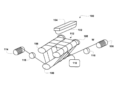
FIG. 1 illustrates an example of a wire saw 100 capable of cutting a single
substrate in
multiple locations in a single pass of the substrate through the wire saw. A
substrate 102,
including, but not limited to, silicon, germanium, gallium arsenide, quartz,
glass may be
provided on a work table 104. To cut the substrate 102, a wire W may be fed
from a supply
reel 106 to a number of rollers 108. The wire W may be wrapped around the
periphery of the
rollers, one or more times, such as in the range of 1 to 200 times, forming a
cutting region
112 between at least two of the rollers. The rollers 108 may include a number
of grooves to
space the wire and a drive motor 110 for driving at least one of the rollers
108. As the rollers
rotate the wire may be moved over and across the rollers 108 through the
cutting region 112.
Eventually, the wire W may leave the cutting region 112 and be wrapped up by a
take up reel
114. The substrate 102 may then be moved towards and through the cutting
region 112 to cut
the substrate into a number of plates or filaments. Tensioning mechanisms 116
and 118 may
be provided to adjust the tension of the wire W before and after the wire
travels through the
cutting region 112. Guides may be provided to aid in guiding the wires between
the supply
reels, tension adjusting mechanism, and/or rollers. A slurry may be provided
in the cutting
region, such that the slurry may contact the substrate. The slurry may, or may
not, include
abrasive particles. In addition, the slurry may provide lubrication and/or
cooling to the cutting
region. Other saws contemplated may include a capstan saw, reel to reel saw or
a filament
saw.
[0030] The size of the kerf produced may be 140 p m or less, and may fall
in the range
of 1 p m to 139 p m, including all values and increment therein. Accordingly,
the kerf may be
of a size of 10 p m to 100 p m, including all values and increments therein.
Again, the kerf
may be understood herein as waste produced during the cutting process. The
kerf may be the
width of the cut, which in some examples, may be affected by the width of the
cutting wire,
the slop in cutting or abrading and the amount of material pulled out from the
sides of the cut.
In a further sense, the present disclosure may, therefore, relate to
workpieces, such as a
polysilicon ingot, which may be cut with the above mentioned wire, where the
kerf produced
may be 140 p m or less, as well as polysilicon wafers produced by any of the
above
referenced wire cutting procedures utilizing the wire disclosed herein and
their associated
alloy chemistries and/or morphology and/or indicated mechanical properties.
13
CA 02751456 2011-08-03
WO 2010/091087
PCT/US2010/023054
Examples
[0031] The
following examples are presented for illustrative purposes and are,
therefore, not meant to limit the scope of the present disclosure herein.
Alloy Design
[0032]
Glass forming iron based chemistries were produced using a variety of casting
methods, with both commercial purity and high purity feedstock. The processing
was
performed in both an inert environment and in air. Using high purity elements,
15 g alloy
feedstocks of the targeted alloys were weighed out according to the atomic
ratio's provided in
Table 1. The feedstock material was then placed into the copper hearth of an
arc-melting
system. The feedstock was arc-melted into an ingot using high purity argon as
a shielding
gas. The ingots were flipped several times and remelted to ensure homogeneity.
After
mixing, the ingots were then cast in the form of a finger approximately 12 mm
wide by 30
mm long and 8 mm thick.
Table 1. Atomic Ratio's for Alloys
Alloy Fe B C Si Ni Co
PC7E7 53.50 16.00 4.50 0.50 15.50 10.00
PC7E8 63.00 12.49 4.54 0.47 16.50 3.00
PC7E8S1A1 67.54 12.49 0.00 0.47 16.50 3.00
PC7E8S1A2 66.04 12.49 1.50 0.47 16.50 3.00
PC7E8S1A3 64.54 12.49 3.00 0.47 16.50 3.00
PC7E8S1A4 63.00 12.49 4.54 0.47 16.50 3.00
PC7E8S1A5 65.54 14.49 0.00 0.47 16.50 3.00
PC7E8S1A6 64.04 14.49 1.50 0.47 16.50 3.00
PC7E8S1A7 62.54 14.49 3.00 0.47 16.50 3.00
PC7E8S1A8 61.00 14.49 4.54 0.47 16.50 3.00
PC7E8S1A9 63.54 16.49 0.00 0.47 16.50 3.00
PC7E8S1A10 62.04 16.49 1.50 0.47 16.50 3.00
PC7E8S1A1 1 60.54 16.49 3.00 0.47 16.50 3.00
14
CA 02751456 2011-08-03
WO 2010/091087
PCT/US2010/023054
PC7E8S1Al2 59.00 16.49 4.54 0.47 16.50 3.00
PC7E8S1A13 61.54 18.49 0.00 0.47 16.50 3.00
PC7E8S1A14 60.04 18.49 1.50 0.47 16.50 3.00
PC7E8S1A15 58.54 18.49 3.00 0.47 16.50 3.00
PC7E8S1A16 57.00 18.49 4.54 0.47 16.50 3.00
PC7E8S8A1 63.30 12.55 4.56 0.00 16.58 3.01
PC7E8S8A2 63.00 12.49 4.54 0.47 16.50 3.00
PC7E8S8A3 62.69 12.43 4.52 0.97 16.42 2.99
PC7E8S8A4 62.37 12.37 4.49 1.47 16.34 2.97
PC7E8S8A5 62.06 12.30 4.47 1.96 16.25 2.96
PC7E8S8A6 61.74 12.24 4.45 2.46 16.17 2.94
PC7E8S8A7 61.43 12.18 4.43 2.96 16.09 2.93
PC7E8S8A8 61.11 12.12 4.40 3.46 16.01 2.91
PC7E8S8A6X1 60.18 12.24 4.45 2.46 16.17 4.50
PC7E8S8A6X2 58.68 12.24 4.45 2.46 16.17 6.00
PC7E8S8A6X3 57.18 12.24 4.45 2.46 16.17 7.50
PC7E9S1A1 61.55 16.49 0.00 2.46 16.50 3.0
PC7E9S1A2 60.05 16.49 1.50 2.46 16.50 3.0
PC7E9S1A3 58.55 16.49 3.00 2.46 16.50 3.0
PC7E9S1A4 57.05 16.49 4.50 2.46 16.50 3.0
PC7E9S1A5 55.55 16.49 6.00 2.46 16.50 3.0
PC7E9S1A1X1 60.05 16.49 0.00 2.46 16.50 4.50
PC7E9S1A1X2 58.55 16.49 0.00 2.46 16.50 6.00
PC7E9S1A1X3 57.05 16.49 0.00 2.46 16.50 7.50
PC7E9S1A1X4 55.55 16.49 0.00 2.46 16.50 9.00
PC7E9S1A1X5 54.05 16.49 0.00 2.46 16.50 10.50
PC7E9S1A1X6 52.55 16.49 0.00 2.46 16.50 12.00
PC7E9S1A1X7 51.05 16.49 0.00 2.46 16.50 13.50
PC7E9S1A1X8 49.55 16.49 0.00 2.46 16.50 15.00
CA 02751456 2011-08-03
WO 2010/091087
PCT/US2010/023054
PC7E9S1A1X9 48.05 16.49 0.00 2.46 16.50 16.50
PC7E9S1A1X10 46.55 16.49 0.00 2.46 16.50 18.00
PC7E9S1A1X11 45.05 16.49 0.00 2.46 16.50 19.50
PC7E9S1A1X12 43.55 16.49 0.00 2.46 16.50 21.00
PC7e10S2A1 65.03 15.00 0.00 0.47 16.50 3.00
PC7e10S1B2 51.01 16.49 0.00 4.00 16.50 12.00
Flat Wire Development
[0033] To
produce relatively flat wire, the ingot fingers produced from the alloy
chemistries in Table 1 were placed in a melt-spinning chamber in a quartz
crucible with a
hole diameter of - 0.81 mm. The ingots were melted in a 1/3 atm helium
atmosphere using
RF induction and then ejected onto a 245 mm diameter copper wheel which was
traveling at
tangential velocities from 5 to 39 m/s. The resulting flat wires (ribbons)
that were produced
had widths which were typically -1.25 mm and thickness from 20 to 140 p m and
lengths that
were in the range of 10 to 30 m. For the purposes of this study, only 10.5 m/s
flat wire date is
presented which typically had thicknesses in the range of 70 to 80 p m. An
example piece of
flat wire (ribbon) which was processed at 10.5 m/s is shown in Figure. 2.
Thermal Analysis of Flat Wire
[0034]
Thermal analysis was done on the as-solidified flat wires using a Perkin Elmer
DTA-7 system with the DSC-7 option. Differential thermal analysis (DTA) and
differential
scanning calorimetry (DSC) as performed at a heating rate of 10 C/minute with
samples
protected from oxidation through the use of flowing ultrahigh purity argon. In
Table 2, the
DSC data related to the glass to crystalline transformation is shown for the
alloys that have
been melt-spun at 10.5 m/s. As can be seen, the majority of samples exhibit
glass to
crystalline transformations verifying that the as-spun state contains
significant fractions of
metallic glass. The glass to crystalline transformation occurs in either one
stage or two stages
in the range of temperature from 366 C to 506 C and with enthalpies of
transformation
from -8.9 J/g to -173.9 J/g.
Table 2. DSC Data for Glass to Crystalline Transformations at 10.5 m/s
16
CA 02751456 2011-08-03
WO 2010/091087
PCT/US2010/023054
Alloy Glass Peak #1 Peak #1 AH Peak #2 Peak
AH
#2
Onset Peak (-J/g) Onset Peak (-J/g)
( C) ( C) ( C) ( C)
PC7E7 Y 468 473 127.2
PC7E8 Y 433 444 46.2 476 481 99.0
PC7E8S1A1 N
PC7E8S1A2 N
PC7E8S1A3 N
PC7E8S1A4 Y 435 450 164.0
PC7E8S1A5 Y 366 403 22.2 461 470 55.3
PC7E8S1A6 Y 422 438 53.2 470 479 107.3
PC7E8S1A7 Y 440 449 24.4 471 477 75.5
PC7E8S1A8 Y 447 455 10.7 471 476 39.4
PC7E8S1A9 Y 427 434 10.0 440 451 85.4
PC7E8S1A10 Y 445 467 122.0
PC7E8S1A11 Y 463 470 117.1
PC7E8S1Al2 Y 466 471 122.0
PC7E8S1A13 Y 451 460 133.1
PC7E8S1A14 Y 461 467 122.3
PC7E8S1A15 Y 470 476 115.9
PC7E8S1A16 Y 506 532 17.0
PC7E8S8A1 Y 432 447 173.9
PC7E8S8A2 Y 433 444 46.2 476 481 99.0
PC7E8S8A3 Y 436 446 38.7 479 485 72.9
PC7E8S8A4 Y 443 453 36.7 485 491 74.0
PC7E8S8A5 Y 453 464 34.9 491 498 64.4
PC7E8S8A6 Y 466 474 49.7 495 507 39.8
PC7E8S8A7 Y 466 475 54.8 504 513 68.0
17
CA 02751456 2011-08-03
WO 2010/091087
PCT/US2010/023054
PC7E8S8A8 Y 476 484 42.0 510 522 14.0
PC7E8S8A6X1 Y 456 464 21.5 488 497 7.8
PC7E8S8A6X2 Y 455 464 13.5 490 498 2.5
PC7E8S8A6X3 Y 455 463 8.9 491 499 1.9
PC7E9S1A1 Y 461 467 60.0 475 480 87.0
PC7E9S1A2 Y 469 475 131.0 606 618 7.7
PC7E9S1A3 Y 476 482 120.0
PC7E9S1A4 Y 496 502 134.0
PC7E9S1A5 Y 497 502 133.0
PC7E9S1A1X1 Y 463 468 50.0 476 483 76.0
PC7E9S1A1X2 Y 462 467 50.0 477 484 81.0
PC7E9S1A1X3 Y 465 473 53.0 479 486 54.0
PC7E9S1A1X4 Y 463 470 49.6 480 487 54.6
PC7E9S1A1X5 Y 465 471 15.2 482 490 15.3
PC7E9S1A1X6 Y 465 472 18.0 483 490 26.0
PC7E9S1A1X7 Y 463 471 25.6 484 491 36.0
PC7E9S1A1X8 Y 466 472 24.0 483 491 34.9
PC7E9S1A1X9 Y 465 472 12.0 487 492 15.9
PC7E9S1A1X10 Y 456 468 24.1 488 494 60.3
PC7E9S1A1X11 Y 461 472 10.3 491 496 15.8
PC7E9S1A1X12 Y 461 473 26.5 492 498 40.6
PC7e10S2A1 Y 395 419 21.4 460 465 55.1
PC7e10S1B2 Y 488 494 60 501 507 35
Overlapping peaks, peak 1 and peak 2 enthalpy combined
Tensile Properties of Flat Wire
[0035] The
mechanical properties of the flat wires were obtained at room temperature
using microscale tensile testing. The testing was carried out in a commercial
tensile stage
made by Fullam which was monitored and controlled by a MTEST Windows software
program. The deformation was applied by a stepping motor through the gripping
system
18
CA 02751456 2011-08-03
WO 2010/091087 PCT/US2010/023054
while the load was measured by a load cell that was connected to the end of
one gripping jaw.
Displacement was obtained using a Linear Variable Differential Transformer
(LVDT) which
was attached to the two gripping jaws to measure the change of gauge length.
Before testing,
the thickness and width of a ribbon were carefully measured at least three
times at different
locations in the gauge length. The average values were then recorded as gauge
thickness and
width, and used as input parameters for subsequent stress and strain
calculation. The initial
gauge length for tensile testing was set at -9 mm with the value determined
after the ribbon
was fixed by measuring the wire span between the front faces of the two
gripping jaws. All
tests were performed under displacement control with a strain rate of -0.001 s-
1. A summary
of the tensile test results including total elongation, ultimate tensile
strength, and Young's
Modulus, is shown in Table 3 for each alloy presented in Table 1 when melt-
spun at 10.5 m/s.
Note that two samples, PC7E8S1Al2 and PC7E8S1A16 were too brittle to test.
Note also
that each sample measurement was performed in triplicate as occasional
macrodefects arising
from the melt-spinning process can lead to localized areas with reduced
properties. As can be
seen in Table 3, the tensile strength values are relatively high and vary from
1.08 GPa to 3.72
GPa while the total elongation values are also very high and vary from 1.72%
to 6.80%.
Table 3 Summary of Tensile Test Results at 10.5 m/s
Ultimate
Total Elongation Tensile Strength Young's Modulus
Alloy (%) (GPa) (GPa)
2.43 2.70 139.0
PC7e7
1.54 1.34 105.7
2.16 1.83 125.0
4.16 2.68 124.6
PC7e8
2.43 1.48 116.1
3.61 2.38 126.1
2.85 1.45 106.2
PC7E8S1A1 3.26 1.68 117.5
2.87 1.42 104.0
19
CA 02751456 2011-08-03
WO 2010/091087
PCT/US2010/023054
2.56 1.41 104.4
PC7E8S1A2
2.07 1.49 131.4
2.43 1.48 131.0
2.98 1.98 130.5
PC7E8S1A3 2.77 1.75 124.2
2.83 1.15 119.3
2.00 1.23 125.1
PC7E8S1A4 3.81 1.38 73.8
2.58 1.19 92.7
3.04 2.01 112.5
PC7E8S1A5 3.94 2.38 121.1
3.21 1.94 112.1
2.33 1.57 123.3
PC7E8S1A6 2.33 1.50 116.1
4.27 2.76 128.7
4.99 2.79 115.3
PC7E8S1A7 4.53 2.49 104.9
4.42 2.74 138.7
3.75 2.09 103.5
PC7E8S1A8 6.09 3.15 119.3
2.40 1.93 129.7
2.80 1.92 137.5
PC7E8S1A9 3.08 1.76 116.3
3.73 2.45 116.3
4.02 2.67 121.6
PC7E8S1A10 3.93 2.54 119.0
CA 02751456 2011-08-03
WO 2010/091087
PCT/US2010/023054
4.02 2.51 117.1
1.72 1.08 119.7
PC7E8S1A11 2.65 1.41 104.4
2.10 1.34 111.6
4.39 2.59 121.1
PC7E8S1A13 3.95 2.42 121.9
4.69 2.42 97.2
4.94 2.40 107.1
PC7E8S1A14 3.38 1.91 113.4
5.66 2.31 82.4
2.16 1.26 109.4
PC7E8S1A15 2.60 1.39 105.8
2.08 1.36 131.4
PC7E8S8A1 5.70 2.47 104.8
3.93 2.11 112.5
5.67 2.15 86.0
4.77 2.35 109.8
PC7E8S8A2
5.66 2.83 113.8
4.57 2.52 100.0
3.05 1.80 106.6
PC7E8S8A3
4.41 2.21 92.7
3.06 1.81 105.7
2.61 1.37 96.8
PC7E8S8A4
2.56 1.51 105.8
2.59 1.37 93.2
5.29 2.58 112.9
PC7E8S8A5 5.24 2.47 100.0
21
CA 02751456 2011-08-03
WO 2010/091087
PCT/US2010/023054
5.94 2.63 96.8
PC7E8S8A6 5.96 2.93 104.8
4.65 2.52 105.8
4.31 3.32 157.4
2.58 2.09 148.5
PC7E8S8A7
5.04 2.98 121.5
4.45 2.75 123.3
6.80 2.69 118.8
PC7E8S8A8 5.17 2.12 104.4
4.92 3.45 149.3
4.87 3.05 124.0
PC7E8S8A6X1 4.33 2.95 144.6
4.26 2.92 115.4
4.45 2.79 132.2
PC7E8S8A6X2
4.77 2.83 120.2
4.21 3.03 125.2
PC7E8S8A6X3 4.07 2.98 148.4
3.71 2.76 139.6
4.33 2.89 147.9
4.67 2.72 114.5
PC7E9S1A1X1
4.77 3.21 142.0
2.72 2.27 164.2
4.51 3.21 146.4
PC7E9S1A1X2
4.27 3.15 152.3
3.84 3.30 172.0
5.58 2.64 105.8
PC7E9S1A1X3
4.77 2.36 110.7
4.45 2.35 117.8
PC7E9S1A1X4 4.59 2.93 123.6
22
CA 02751456 2011-08-03
WO 2010/091087
PCT/US2010/023054
4.62 2.91 134.5
4.25 3.34 153.2
4.64 3.19 151.5
PC7E9S1A1X5 5.66 3.70 129.2
4.31 2.76 122.7
4.07 3.17 152.7
PC7E9S1A1X6
5.11 2.97 128.4
3.82 2.90 149.9
4.46 3.09 140.6
PC7E9S1A1X7
5.17 2.80 133.7
3.87 3.16 156.1
4.65 3.07 131.8
PC7E9S1A1X8
3.87 3.12 154.2
4.30 3.13 162.7
5.36 2.93 133.5
PC7E9S1A1X9
4.28 2.75 141.6
3.87 3.17 156.2
3.89 2.52 152.3
PC7E9S1A1X10
3.91 2.67 156.0
3.66 3.07 161.1
4.05 2.38 111.9
PC7E9S1A1X11
3.97 2.66 118.8
2.98 2.39 128.5
4.35 2.85 127.2
PC7E9S1A1X12
4.33 2.58 118.2
4.60 2.67 113.2
PC7E10S2A1 3.24 2.15 107.61
4.29 2.86 113.56
23
CA 02751456 2016-10-21
3.83 2.74 121.38
5.46 3.72 104.21
PC7E10S1B2 4.02 3.63 135.32
4.08 3.71 126.31
Circular Cross Sectional Wire
[0036] Using a Taylor-Ulitovsky wire making process, numerous runs of
two alloys,
PC7E10S2A1 and PC7E10S1B2 listed in Table 1 were produced. Note that the two
alloys
were processed into ingots and cast into fingers in a similar fashion to those
utilized for flat
wires. Approximately 20 small representative Taylor-Ulitovsky wire making runs
(averaging
- 300 m) were produced at various conditions including with and without water
cooling, and
at various thickness's from -3 to -50 gm in diameter. Additionally, six longer
lengths of
wire were produced and put onto spools. The wire lengths, total diameters and
glass coating
thickness's can be seen in Table 4. In Figure 3, a picture can be seen of the
spool which is
shown of glass coated microwire of Run #6.
Table 4 Details of Taylor-Ulitovsky Glass Coated Wire Production
Run # Alloy Wire Length, Total Wire Metal Core
(m) Diameter, (gm) Diameter, (gm)
Spool #1 PC7e10S1B2 1000 22-23 17 - 18
Spool #2 PC7e10S1B2 5000 3 - 5 2 - 3
Spool #3 PC7e10S2A1 1500 24 - 26 17 - 18
Spool #4 PC7e10S2A1 700 22 - 23 17 - 18
Spool #5 PC7e10S2A1 1650 21-23 17 - 18
Spool #6 PC7e10S2A1 600 45 - 50 43-47
Thermal Analysis of Circular Cross Sectional Wire
[0037] Thermal analysis was performed on the as-solidified glass coated
microwires
using a Perkin ElmerTM DTA-7 system with the DSC-7 option. Differential
thermal analysis
(DTA) and differential scanning calorimetry (DSC) was performed at a heating
rate of
24
CA 02751456 2011-08-03
WO 2010/091087
PCT/US2010/023054
C/minute with samples protected from oxidation through the use of flowing
ultrahigh
purity argon. In Table 5, the DSC data related to the glass to crystalline
transformation is
shown for selected circular cross sectional glass coated microwires which have
been
processed with and without water cooling. As indicated, all samples exhibit
relatively large
5 glass to crystalline transformations, which may indicate that the as-
solidified wire state
contains significant fractions of metallic glass. Note that the values of
crystallization
enthalpy are lowered, which may be due to the fact that the wire were measured
with the
glass coating intact. In Figures 4 and 5, the water cooled and non water
cooled DTA curves
are shown for the PC7E10S2A1 and PC7E10S1B2 alloys respectively. As can
clearly be
10 seen in the Figures, the alloys are insensitive to processing condition
and the presence of
water cooling due to their inherent high level of glass forming ability. In
Figures 6 and 7, the
DTA curves are compared for the PC7E10S2A1 and PC7E10S1B2 wires respectively
which
are in both flat wire (ribbon) and glass coated circular wire forms. As shown
in these
Figures, the crystallization and melting peaks are similar, indicating that
very similar
chemistries and structures were achieved for each alloy in both a flat wire
(ribbon) and glass
coated circular wire.
Table 5 Thermal Analysis Summary For Glass Coated Microwires
Alloy Water Crystallization Peaks
Cooling Peak #1 Peak #2
Onset Temp AH Onset Temp AFT
( C) ( C) (-J/g) ( C) ( C) (-J/g)
PC7E10S2A1 Y 385 406 9.8 465 472
35.5
PC7E10S2A1 N 389 411 23.8 470 478
32.0
PC7E10S1B2 Y 478 487 -- 503 510
69.1*
PC7E10S1B2 N 487 492 -- 502 509
84.3*
= AH from peaks 1 and 2 due to overlapping nature
SEM Analysis of Circular Cross Sectional Wire
[0038] To
examine the structure of the circular cross sectional wires, scanning
electron microscopy (SEM) was performed on selected samples. The structure of
the samples
CA 02751456 2011-08-03
WO 2010/091087
PCT/US2010/023054
was observed using a Zeiss EVO-60 scanning electron microscope with an
electron beam
energy of 17.5kV, a filament current of 2.4 A, a spot size setting of 1000. In
Figure 8, a
backscattered electron image (B SE) is shown of microwire from Spool # 6
showing the wire
with the glass coating intact. In Figure 9, a BSE image is shown of the Spool
# 6 microwire
showing the wire with the glass coating and with the coating removed near the
tip showing
the bare wire. In Figure 10, a high magnification BSE image is shown of the
microwire of
Spool #6 showing a close-up of the wire structure with the glass coating
removed. Consistent
with the DTA / DSC results, the structure is not expected to be resolved due
to the primarily
glass nature of the wires. However, nanoscale structures which may or may not
be present
would not be expected to be resolved due to the resolution limits inherent
with backscattered
electron detection.
Tensile Testing of Circular Cross Sectional Wire
[0039]
Initial measurements of the glass coated microwires were obtained at room
temperature using microscale tensile testing in the same system and with a
similar
methodology as presented before for the flat wire samples. The main difference
was that the
existing load cell (1,000 lb) appeared to be too large to measure single wire
specimens. In
this case, measurements were performed utilizing a twisted wire rope. For
Spool #6, ninety
lengths of wire were cut and then all ninety wires were twisted together to
form a wire rope
as shown in Figure 11.
[0040]
Tensile testing was performed and the resulting cordage was examined in the
SEM. The cross sectional areas of the actual wires were measured and the
number of wires
broken was counted. This allowed an estimate of the tensile strength values as
shown in
Table 6. Note that the tensile elongation values are not presented since in
some cases,
individual wires appeared to slip during the testing, resulting in anomalously
high and
inaccurate elongation values. Based on the DTA, SEM, and measured tensile
strength values,
it is believed that a very similar structure is obtained in the PC7E10S2A1 and
PC7E10S1B2
alloys in both flat wire and glass coated circular wire forms. Thus, it is
believed that the
tensile elongation values would also be similar. It is possible and perhaps
probable that the
tensile properties of the circular wire are higher than the flat wire since
the circular cross
section which would be expected to be more favorable for shear band
interaction. An
indication of this is shown in Figure 12 where the interacting shear bands of
a wire from
26
CA 02751456 2011-08-03
WO 2010/091087
PCT/US2010/023054
Spool #6 can be clearly seen after this wire was put under tension and then
twisted to
introduce both tensile and torsional strains.
Table 6 Tensile Results For Glass Coated Microwires
Sample Geometry
Core Diameter, # of Microwires Gage Length, Tensile Strength,
Test # (Pm) in a Rope MITI GPa
1 28-35 90 7.92 4.5
2 28-35 90 8.06 4.2
TEM Studies on Glass Coated Microwire
[0041] To
examine the microstructures in microwires, TEM microscopy was used.
To obtain an electronic-transparent area for TEM observation, samples of the
Spool #6
PC7E10S2A1 wires were mounted on a copper disk. The resulting sample was ion
milled
using a Gatan Precision Ion Polishing System (PIPS) which was operated at an
ion beam
energy level of ¨ 4 keV. The ion beam incident angle was 100 first, then
reduced to 7 after
penetration, and finished up by further reducing 4 . After ion milling, some
fractions of the
wires had thin areas appropriate for TEM microscopy. In Figure 12, TEM
micrographs are
shown of the Spool #6 PC7E10S2A1 microwire with both pictures taken at
different
magnification in thin areas near the center of the wire. In the left hand
corners of both
micrograph of Figure 13, selected area diffraction patterns are shown. As
seen, from the
diffraction pattern, the structure of the wire is found to be primarily
amorphous with
individual crystalline phases seen from their diffraction spots. As seen by
the micrograph,
the small crystalline phases or clusters are very small and typically in the
range of 1 to 3 nm.
Due to the uniformly small structure, it is believed that these small
crystalline phases /clusters
form through a spinodal type transformation. The structure of the wire can
thus be described
as a spinodal glass matrix microconstituent structure since isolated
crystalline phases /
clusters exist in a glass matrix.
[0042] The
foregoing description of several methods and embodiments has been
presented for purposes of illustration. It is not intended to be exhaustive or
to limiting and
many modifications and variations are possible in light of the above
teachings.
27