Note: Descriptions are shown in the official language in which they were submitted.
CA 02752746 2011-08-16
MEMS DEVICE WITH INTEGRATED VIA AND SPACER
FIELD OF THE INVENTION
Embodiments of the present invention relate to MEMS manufacturing process of
MEMS device for achieving high interconnect density while providing a
precision control
of the spacer with flexible subsequent manufacturing processes. More
particularly
embodiments of the present invention relates to a method of making MEMS device
arrays.
BACKGROUND OF THE INVENTION
Currently, the MEMS dual-axis mirrors involve a precision spacer and electrode
layer. This has been done by multiple wafer bonding process, resulting in poor
manufacturing yield. The invention replaces the spacer-electrode stack with
one spacer-
VIA substrate. This process allows a variety of bonding methods for the
subsequent
processes, thus reducing the complexity of the fabrication process and
improving the
overall yield. The MEMS technology finds its applications in optics in which a
small-
size mirror (micromirror) in the order of 10 m to 500 m can be actuated by
applied
voltages. There are numerous prior arts on the mirror structures (found
citations). In
general, two-axis mirrors are more useful because the mirrors can steer the
optical beam
in two dimensions. Usually, these designs involve double hinges with gimble.
There are
two classes of actuator designs. The first class is to have the actuators on
the same
surface of the MEMS mirror layer but outside the optical region. Examples of
these types
of actuators include comb drive or thermal actuators. The second class is to
have the
actuator underneath the MEMS mirrors. These types of actuators are, in
general,
electrostatic. The structures of the second class is more commonly adopted in
the
applications requiring high-fill-factor and/or high-density mirrors. One
example of these
is described in U.S. Pat. No. 6,984,917 and is illustrated in FIG. 1.
As shown in FIG. 1, a mirror 1 and frame 2 are formed from a common sheet of
material. The mirror 1 is connected to the frame 2 by a thin member 3 formed
from the
sheet of material. The thin member 3 lies along an axis of rotation that lies
perpendicular
to the plane of the drawing in FIG. 1. The thin member 3 acts as a torsional
spring hinge.
The mirror 1 is suspended over cavity 4 so that it is free to rotate.
Electrodes 5A and 5B
are disposed in the cavity 4. Electrodes 5A and 5B underlie a portion of the
mirror 1,
with one electrode on each side of an axis-of-rotation defined by the thin
member 3.
CA 02752746 2011-08-16
2
When an electrical potential is applied between a mirror 1 and one of the
underlying electrodes 5A, 5B, the cradle rotates out-of-plane, i.e., out of
the plane defined
by the support frame 2, about its axis of rotation toward the electrified
electrode.
Torsional forces developed by the thin member 3 tend to counteract the
electrostatic force
between the attractive electrode and cradle. The mirror 1 can rotate about the
axis
defined by the thin member 3 by an angle y that depends on the voltages
applied to the
electrified electrode the separation of the mirror and the electrode and the
torsional
stiffness of the hinge. The direction of rotation depends on which electrode
is electrified.
For example, if an electric potential is applied between mirror 1 and
electrode 5B, mirror
1 rotates out-of-plane of frame 2 about axis X such that the portion of mirror
1 that
overlies electrode 5B moves downward toward that electrode.
In a device of the type shown in FIG. 1, the electrodes 5A and 5B should be
electrically isolated from each other to avoid large currents between them
when a voltage
is applied. In fact, in order to allow the mirror to tilt in both clockwise
and
counterclockwise in FIG. 1, two electrodes are needed. For dual-axis
operation, 3 or 4
electrodes are needed. To ease the control algorithm, 4 electrodes per mirror
are often
employed.
Since the device is operated by electrostatic force, a physical gap between
the
electrodes and the mirror is very critical. This gap needs to be controlled
with high
precision to ensure the performance of the device. Typically, with a smaller
gap, less
voltage is needed to tilt the mirror to a certain angle. However, the maximum
angle
(before a snapping behavior occurs) is smaller. With a larger gap, higher
voltage is
needed to tilt the mirror to a certain angle, but the maximum angle is also
enlarged.
Therefore, there exists an optimal gap for each application.
While a through-wafer interconnect is commercially available, an integrated
solution is not available without this integrated spacer. In order to access
the electrodes
underneath the MEMS mirror, a dedicated electrode layer is used to bring the
electrical
contact to a region with no MEMS mirror, followed by an access etch from the
top
structure. This consumes a significant portion of the area of the wafer on
which MEMS
mirrors are formed, reducing the number of dies per wafer. Using commercially
available vias or through-wafer interconnects can change the interconnect
direction from
lateral to vertical. However, it does not integrate a spacer layer with
sufficient thickness
CA 02752746 2012-01-03
r
3
accuracy for the device operation. It turns out that combining an integrated
spacer with a
vertical interconnect substrate provides a large degree of process latitude.
Competitors
will have to build a spacer layer on top of the VIA wafer. The choice of the
processes
and materials will limit the choices of the subsequent process.
For example, if an organic material is selected, the subsequent process
temperature will be limited.
In many applications, high density of micromirrors is required, either in 1 xN
or
NxM format. The number of the mirrors increases the number of the controlling
electrodes. For dual-axis operation, three or four electrodes may be needed
for each
micromirror. Therefore, for example, for a 10 x 10 micromirror array, the
number of
electrodes can be as large as 300 to 400.
As seen in FIG. 1, the electrodes are under the micromirrors. Therefore, there
must be an electrical connection (interconnect) between the bond pads to the
electrodes.
In most cases, the size of the bond pads is larger than the size of the
micromirrors. This
causes the useable area of the overall die to be a small fraction of the
entire die area, thus
greatly reducing the number of dies per wafer. As an example to illustrate
this issue,
FIG. 2 shows a top view of a MEMS 1 xN micromirror array. Since the pitch of
the
micromirrors is typically narrower than the pitch of the bond pads for
standard wire
bonding process, a fan-out-shaped interconnect region 6 is used to
electrically connect an
optical region 7 and a bond pad region 8. As may be seen from FIG. 2, the real
estate of a
MEMS wafer is not fully utilized by this approach. One approach to resolve the
foregoing real estate issue is to perform the interconnect in the vertical
direction by
putting the electrode contacts of the bond pad region 8 on the backside of the
MEMS
wafer with electrical connection to the driver electronics by a solder bump
process. The
solder bump process, developed for flip-chip assembly for Silicon (Si) CMOS,
offers a
much higher interconnect density. In order to bring the electrical contact
vertically, it is
possible to integrate a commercially available through-wafer interconnect
technology.
Examples of such interconnect technology are described, e.g., in U.S. Patent
Application
Publications Numbers 20080122031, 20080157339, and 20080157361.
A typical through-wafer interconnect is shown in FIG. 3. The through-wafer
interconnect technology may also be made by a standard MEMS fabrication
process.
First, through holes may be formed through a substrate 9, such as a Silicon
(Si) wafer,
CA 02752746 2012-01-03
4
followed by depositing insulating passivation layer 10 on the sidewalls of the
holes.
Then, a conducting material 11 is used to fill the remaining holes. The holes
may be
formed by an anisotropic etch process such as Deep Reactive Ion Etching
(DRIE). The
insulating passivation layer is typically thermally grown SiO2. But, other
deposition
techniques (PECVD, CVD) may also be used.
The choices of the conducting materials are based on the applications. For
applications in which conductivity is important, electroplated metals are
commonly used.
If low conductivity is acceptable, poly silicon is commonly used for the
benefit of similar
thermal expansion coefficient with the substrate.
An example of a MEMS micro-gyroscope using a through-wafer interconnect
described in U.S. Pat. No. 7,015,060 to Kubena, is shown in FIG. 4. The
gyroscope is
formed using four wafers. A resonator 23 is formed from a top silicon layer of
a silicon-
on-insulator (SOI) wafer. A post 12 is formed from a bottom silicon layer of
the SOI
wafer. A second wafer bonded to the first wafer is used to form another post
13. A third
wafer 14 having a silicon substrate 15 is etched to form pillars and through
holes. The
substrate 15 is oxidized to coat its front and back surfaces and line the
walls of the
through holes with a layer of SiO2 16. Electrically conductive interconnects
17 are
formed by filling the through holes with metal. In this case, electroplated
copper or
copper alloy were preferred for the conducting material owing to the
electrical
requirements of the device. Metal is formed over the pillars and interconnects
17 and
patterned to form electrodes connected to the interconnects. A hole is then
made in the
third wafer 14 to receive the post 13. The resonator 23 is then bonded to the
third wafer
14 at the metal on the pillars. A cavity 18 is formed in a base layer 19 of a
fourth wafer
20 (another SOI wafer) to accommodate the resonator 23 and post 12. The fourth
wafer
20 is then bonded to the third wafer 14 using a sealing ring metal 21 and a
solder 22. The
fourth wafer 20 acts as a cap for the resonator 23. As seen in FIG. 4, the
through-wafer
interconnect is much more complicated than that in FIG. 2. This is because it
is not
straightforward to integrate the vertical interconnect concept directly to the
various
operating modes of MEMS devices.
Specifically, if a MEMS mirror device of the type shown in FIG. I were to be
combined with a vertical through-wafer interconnect, the mirror, it would be
desirable to
CA 02752746 2011-08-16
precisely control the spacing between the layer from which the mirror is
formed and the
electrodes located underneath the mirror and on top of the through-wafer
interconnects.
Unfortunately, such precision is difficult to obtain with high yield using a
process like
that described in U.S. Pat. No. 7,015,060.
5 There are also challenges to utilizing through-wafer interconnects in a
micromirror array application. These challenges include, e.g., the density of
the
interconnect, the locations of electrode, and the requirements for precision
for the gap
between the electrodes and the mirrors. The pitch of the micromirror array
typically is
between 50 m to 500 m. The pitch of the standard solder bump process is
typically
around 200 m. If 4 electrodes are needed for each mirror, clearly some form
of routing
is required to distribute the electrodes from the patterns, required by the
operation of the
MEMS devices, to the contact patterns acceptable for the solder bump process.
It is within this context that embodiments of the present invention arise.
SUMMARY
The disadvantages of the prior art are overcome by embodiments of the present
invention directed to a method for fabricating a microelectromechanical system
(MEMS)
device and a MEMS device.
According to a first embodiment, one or more conductive vias may be formed
through a lower layer of a bottom substrate having an insulating layer
sandwiched
between an upper layer and the lower layer. Each of the vias is electrically
isolated from
the lower layer. The vias are electrically connected to one or more
corresponding
electrical contacts formed on a back side of the lower layer. One or more
portions of the
upper layer that overlie the one or more vias are selectively removed to form
one or more
device cavities. A device layer is bonded to the bottom substrate. One or more
devices
are formed from the device layer. Each of the devices overlies a corresponding
one of the
device cavities. Each of the devices is connected to the rest of the device
layer by one or
more corresponding hinges formed from the device layer. Each of the devices is
electrically isolated from the vias.
In some versions of the first embodiment one or more device electrodes may be
formed in the one or more device cavities, after forming the device cavities
and before
connecting the vias to the contacts. Each device electrode may be electrically
connected
to a corresponding one of the vias. In such versions, the device electrodes
may be formed
CA 02752746 2011-08-16
6
on one more portions of the insulating layer that have been exposed by removal
of the
one or more portions of the upper layer.
In some versions of the first embodiment, the bottom substrate may be a
silicon
on insulator substrate.
In some versions of the first embodiment, the device may be formed by removing
selected portions of the device layer to form the devices and hinges.
In some versions of the first embodiment the one or more devices may include
one or more mirrors.
In some versions of the first embodiment, forming the cavities may include
protecting the back side of the lower layer during removal of the selected
portions of the
upper layer.
In some versions of the first embodiment, the device layer may be a layer of a
top
substrate having an insulator layer sandwiched between the device layer and an
additional
layer. In such versions, the additional layer may be removed before forming
the devices.
In some versions of the first embodiment, the device layer and bottom
substrate
may be bonded by a high-temperature bonding process. In such versions an
electrically
conductive bonding material may be disposed on the electrical contacts formed
on a back
side of the lower layer after bonding the device layer to the bottom
substrate.
In some versions of the first embodiment, the device layer and bottom
substrate
may be bonded by a low-temperature bonding process. In such versions an
electrically
conductive bonding material may be disposed on the electrical contacts formed
on a back
side of the lower layer before bonding the device layer to the bottom
substrate.
According to a second embodiment, a microelectromechanical system (MEMS)
device may comprise a bottom substrate and a device layer bonded to the bottom
substrate. The bottom substrate has an insulating layer sandwiched between an
upper
layer and a lower layer. One or more conductive vias are formed through the
lower layer
at locations that underlie the one or more device cavities. Each via is
electrically isolated
from the lower layer. One or more portions of the upper layer have been
selectively
removed to form one or more device cavities. One or more devices are formed
from the
device layer. Each device overlies a corresponding device cavity. Each device
is
connected to the rest of the device layer by one or more corresponding hinges
formed
CA 02752746 2011-08-16
7
from the device layer. One or more electrical contacts are formed on a back
side of the
lower layer. Each contact is electrically connected to a corresponding
conductive via.
In some versions of the second embodiment, the bottom substrate maybe a
silicon
on insulator substrate.
In some versions of the second embodiment, selected portions of the mirror
layer
have been removed to form the devices and hinges.
In some versions of the second embodiment, the one or more devices include one
or more mirrors.
In some versions of the second embodiment, one or more device electrodes may
be formed in the one or more device cavities. Each device electrode may be
electrically
connected to a corresponding one of the one or more vias. In such versions,
the device
electrodes may be formed on one more portions of the insulating layer that are
exposed
by removal of the one or more portions of the upper layer to form the one or
more
cavities.
BRIEF DESCRIPTION OF THE DRAWINGS
FIG. 1 is a cross section view of MEMS mirror of the prior art (prior art,
U.S. Pat.
No. 6,984,917)
FIG. 2 is an example of the top view of a MEMS 1 xN micromirror array
according to the prior art.
FIG. 3 is a cross section of a typical through-wafer interconnect of the prior
art.
FIG. 4 is an example of using through-wafer interconnect for a MEMS device of
the prior art.
FIG. 5 through 19 are a sequence of cross-sectional drawings detailing the
process
of manufacturing a MEMS device according to an embodiment of the present
invention.
DESCRIPTION OF THE SPECIFIC EMBODIMENTS
Although the following detailed description contains many specific details for
the
purposes of illustration, anyone of ordinary skill in the art will appreciate
that many
variations and alterations to the following details are within the scope of
the invention.
Accordingly, the examples of embodiments of the invention described below are
set forth
without any loss of generality to, and without imposing limitations upon, the
claimed
invention.
INTRODUCTION
CA 02752746 2011-08-16
8
In embodiments of the present invention through-wafer interconnects may be
integrated with a bottom substrate that provides a precise spacer layer in a
MEMS device.
The spacer layer is sometimes herein referred to as a Spacer with Through
Wafer
Interconnects (STW)
MEMS DEVICE FABRICATION
By way of example, and not by way of limitation, FIG. 5 through FIG. 19
illustrates a possible sequence of operations for manufacturing a MEMS device
according
to an embodiment of the present invention. It is noted that in FIG. 5 through
FIG. 19, the
dimensions are not drawn to scale. In particular, the layer thicknesses and
widths have
been drawn to be visible to illustrate the relevant concepts. In the example
illustrated in
FIG. 5 through FIG. 19, a 1 xN array is depicted for the sake of simplicity
and clarity.
Those of skill in the art will recognize that embodiments of the invention are
not limited
to 1 xN configurations.
The manufacturing process may be broken down into three major parts: 1)
fabrication of a bottom (STW) substrate; 2) fabrication of a device layer on
another
substrate (e.g., an SOI substrate); and 3) bonding the bottom substrate and
device layer
together and releasing the devices.
As shown in FIG. 5, the process of fabricating the STW starts with a bottom
substrate 101 having an insulating layer 103 between a top layer 102 and a
bottom layer
104. The top layer 102 and bottom layer 104 may be made of electrically
conducting or
semiconducting materials. By way of example, the bottom substrate may be a
commercially available Semiconductor on insulator (SOI) wafer, e.g., having a
silicon
dioxide (Si02) layer sandwiched between upper and lower layers made of
silicon. The
thicknesses of the top layer 102 and the underlying insulating layer 103 can
be precisely
obtained, owing to the advanced wafer polishing processes used in the
fabrication of SOI
wafers. The thickness of the top layer can be from a few microns to hundreds
of microns.
By way of example, the thickness of the bottom layer 104 may be on the order
of 500 m
to provide sufficient strength to avoid breaking the substrate during
subsequent
fabrication processes. However, when necessary, the substrate 101 may be made
thinner
to ease the through-wafer etching process.
CA 02752746 2011-08-16
9
In the embodiment illustrated, processing of the bottom layer is performed
first.
To avoid damage to the top layer 102 during the processing of the bottom layer
104, it is
common to deposit some protection layer on the exposed surface of the top
layer 102
(sometimes referred to herein as the front side). Examples of suitable
materials for the
top protection layer include, but are not limited to, polymers, silicon
dioxide, silicon
nitride and metals. However, for simplicity, this protection process is not
illustrated here.
The exposed surface of the bottom layer 104 (sometimes referred to herein as
the
backside) may be patterned by standard photolithography to form an etching
mask. The
bottom layer 104 is then etched from the backside through one or more openings
in the
mask to form one or more through holes 105, as shown in FIG. 6. By way of
example, an
anisotropic etch, e.g., a Deep Reactive Ion Etch (DRIE), may be used to etch
the through
holes 105. The etch process may have sufficient etch selectivity that the
insulating layer
103 acts as an etch stop.
For example, depending on the etch process used, the etch rate of SiO2 and Si
can
be very different silicon and silicon dioxide (for example, an Si02:Si etch
selectivity of
1:100). When an SOI wafer having SiO2 between top and bottom silicon layers is
etched
using such an etch process the SiO2 layer can serve as an etch stop. In FIG.
6, the etched
holes are illustrated with straight side walls 106. However, in reality, the
sidewalls may
not be straight in the microscopic scale.
After a thorough clean, a layer of insulating material 107 (e.g., SiO2) maybe
formed on the backside of the bottom layer 104 and the sidewalls 106 of the
through
holes 105, as shown in FIG. 7. By way of example, the insulating layer 107 may
include
a thermally grown oxide to ensure a good coverage. However, since the growth
rate of
thermal oxide is very slow, additional insulating material may be deposited on
top of the
thermal oxide to increase the breakdown voltage between the bottom substrate
and
electrodes that are subsequently deposited on the insulating layer 107.
Conductive material 108 is then deposited or otherwise formed to coat the back
side of the bottom substrate 104 and fill or coat the through holes, as shown
in FIG. 8.
Conductive material in the holes provides conductive vias 109 that are
electrically
insulated from the bottom substrate by the insulating material 107. The size
of the
through holes 105 is often a crucial parameter depending on the process used
to form the
conducting material 108. For example, if electroplating is used, sometimes
voids may
CA 02752746 2011-08-16
form due to necking of the opening of the holes. Poly-silicon is a good
conductive
material for achieving good coverage because it can be deposited by chemical
vapor
deposition (CVD). After the forming the conducting material 108, the backside
may not
be as smooth as depicted in FIG. 8. For further lithography process, a polish
step may be
5 implemented to planarize the back side and at the same time remove the
conducting
material outside the hole area as depicted in FIG. 9.
After the planarization, an interconnect metal may be deposited and patterned
to
form one or more electrodes 110 that are in electrical contact with the vias
109, as
illustrated in FIG. 10. Another insulating layer 111 may be subsequently
deposited on the
10 backside of the bottom layer 104 and patterned as shown in FIG. 11. The
insulating layer
may be patterned so that bump pad areas of the electrodes 110 are exposed.
Conductive
bump material 112, e.g., a solder, may be selectively deposited on the bump
areas that are
exposed by openings in the second insulating layer 111, as shown in FIG. 12.
Optionally,
the bump material may be deposited at a later stage of manufacture if it is
convenient. It
is also possible to use a jet print process to apply a conducting epoxy
instead of solder
bump. Furthermore, it is noted that the interconnect metal 110 and insulating
layer 111
may also be formed and patterned at a later stage of fabrication, as discussed
below.
Once the vias 109 have been formed, processing of front side of the bottom
substrate 101 may begin. After flipping over the bottom substrate 101 and
removing the
protection layer, a portion of the top layer 102 may be selectively removed,
e.g., through
a combination of photolithography and etching processes, leaving a gap 113
that exposes
a portion of the insulating layer 103, as shown in FIG. 13. Because the
thickness of the
top layer 102 may be precisely controlled (e.g., less than 0.5 m) during the
fabrication of
the bottom substrate 101, the etching of the top layer 102 produces a gap
having a precise
thickness (e.g., less than 0.5 m).
The thickness precision of the top layer 102 can be within 0.05 um for layers
less
than 5 gm and within 0.3 m for thicker layers. The precision of the thickness
of the gap
113 may be the same for similar ranges of gap thickness. Preferably, the
thickness
precision of the gap 113 is better than 0.5 m.
As shown in FIG. 14, selected portions of the insulating layer 103 of the
bottom
substrate 101 may be removed to expose the conductor in the holes that form
the vias
109. Note that, because of the interconnect metal on the back side, the
location of the
CA 02752746 2011-08-16
11
through-holes may be conveniently located. One possibility is to use the
conductive vias
109 (i.e., the conductive material in the through holes) as controlling
electrodes for device
operation. However, it may be desirable to use another conducting layer to
form an
electrode pattern. In such a case electrically conductive electrode material
114 may be
deposited on exposed portions of the insulating layer 103 in electrical
contact with the
vias 109 and patterned to form electrodes as depicted in FIG. 15.
A device structure is fabricated on a separate substrate 115, referred to
herein as a
device substrate. One or more MEMS devices are fabricated from the device
substrate.
By way of example, and not by way of limitation, the MEMS devices may be MEMS
mirrors. However, in alternative embodiments other MEMS devices may be
fabricated.
Examples of other MEMS devices include, but are not limited to,
accelerometers,
gyroscopes, pressure sensors, chemical sensors and switches.
There are many design options for the device structure and the device
substrate.
By way of example, and not by way of limitation, the device substrate 115 may
be a
composite wafer, e.g., a SOI wafer, having an insulator layer 117 sandwiched
between a
top layer 116 (referred to herein as a device layer) and a bottom layer 118.
The thickness
of the top layer 116 may be designed for optimal device performance.
The next step is to combine the bottom substrate 101 and the device substrate
115
together. There are multiple ways to perform this operation. One of the
advantages of an
approach based on SOI is that the entire substrate may be made mostly of
silicon with a
small proportion of dissimilar materials. This allows a very wide processing
temperature
window.
For example, if fusion bonding is chosen (in which a process temperature as
high
as >10000 C.), the filling conducting material 108 that forms the vias 109 may
be
polysilicon. The interconnect metal 110 and insulating layer 111 can be formed
and
patterned after the bonding process is completed. However, if a low
temperature bonding
process is chosen, such as eutectic bonding, a bonding material can be
deposited after the
back side processes are completed as shown in FIG. 16.
The bonding process may combine the bottom substrate 101 and device substrate
115 together with their respective top layers 102, 116 facing each other as
shown in FIG.
17. The thick bottom layer 118 of the device substrate 115 provides structural
support for
the device layer 116 and insulating layer 117 during the bonding process.
After bonding,
CA 02752746 2011-08-16
12
a standard process may be used to remove the bottom layer 118 of the device
substrate
115 as depicted in FIG. 18. The exposed surface of the insulating layer 117
(or, if part of
the insulating layer is removed, an exposed underside of the device layer 116)
may then
be patterned to define a device 119 to be formed from the device layer 116 of
the device
substrate 115. The device is formed over a cavity formed by the gap 113
between the
insulator layer 103 of the bottom substrate 101 and the device layer 116 of
the device
substrate 115. The thickness of the cavity may be made to a desired precision
as long as
the thickness of the top layer 102 was sufficiently precisely controlled
during initial
fabrication of the bottom substrate 101.
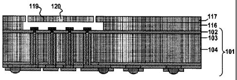
The device 119 may be released from the top layer 116 by another etching
process
that removes selected portions of the device layer 116 as illustrated in FIG.
19. The
device 119 may be connected to other portions of the device layer 116 by one
or more
thin portions 120 that can act as torsional hinges. The device 119 is
electrically isolated
from the electrodes 114 and vias 109 by the insulating layer 103 and
insulating material
107. When a voltage is applied to one of the electrodes 114 the device may
rotate about
the hinges 120 toward the electrode 114. The precise thickness of the top
layer 102 of the
bottom substrate 101 provides a precise gap between the device 119 and the
electrodes
114.
Embodiments of the present invention provide a novel approach to realize a
MEMS device structure with improved yield (number of dies per wafer) and a
much
larger process flexibility. Although fabrication of a single is shown for the
sake of
clarity, those of skill in the art will realize that the process described
above may be
extended to simultaneous fabrication of an arbitrary number of devices on a
common
substrate.
While the above is a complete description of the preferred embodiment of the
present invention, it is possible to use various alternatives, modifications
and equivalents.
Therefore, the scope of the present invention should be determined not with
reference to
the above description but should, instead, be determined with reference to the
appended
claims, along with their full scope of equivalents. Any feature, whether
preferred or not,
may be combined with any other feature, whether preferred or not. In the
claims that
follow, the indefinite article "A" or "An" refers to a quantity of one or more
of the item
following the article, except where expressly stated otherwise. The appended
claims are
CA 02752746 2011-08-16
13
not to be interpreted as including means-plus-function limitations, unless
such a
limitation is explicitly recited in a given claim using the phrase "means
for."