Note: Descriptions are shown in the official language in which they were submitted.
CA 02753373 2011-08-22 110214:910353
DESCRIPTION
TITLE OF THE INVENTION
Silicon Carbide Substrate
TECHNICAL FIELD
The present invention relates to a silicon carbide substrate.
BACKGROUND ART
Recently, a SiC (silicon carbide) substrate has been introduced as a
semiconductor substrate used for manufacturing semiconductor devices. As
compared
with more widely used Si (silicon), SiC has wider bandgap. Therefore, a
semiconductor device using a SiC substrate has advantages such as high
breakdown
voltage and low on-resistance and, in addition, its property does not much
degrade in
high-temperature environment.
In order to enable efficient manufacturing of semiconductor devices, the
substrate must be of a certain size or larger. According to United States
Patent No.
7,314,520 (Patent Document 1), it is possible to manufacture a SiC substrate
having the
size of at least 76 mm (3 inches).
PRIOR ART DOCUMENTS
PATENT DOCUMENTS
Patent Document 1: United States Patent No. 7,314,520
SUMMARY OF THE INVENTION
PROBLEMS TO BE SOLVED BY THE INVENTION
Industrially available size of SiC single crystal substrate is about 100 mm (4
inches) at the largest and, therefore, it has been difficult to efficiently
manufacture
semiconductor devices by using a large single-crystal substrate. When
characteristics
of a plane other than the (0001) plane are to be utilized in hexagonal system
SiC, this
poses a particularly serious problem. This will be discussed in the following.
A SiC single crystal substrate with a very small number of defects is
typically
-1-
CA 02753373 2011-08-22 110214:910353
manufactured by cutting a SiC ingot obtained through surface growth of the
(0001)
plane that is less susceptible to stacking fault. Therefore, it follows that a
single crystal
substrate having plane orientation other than the (0001) plane is cut not
parallel to the
surface of growth. As a result, it becomes difficult to ensure the full size
of single
crystal substrate, or to effectively make use of large part of the ingot.
Consequently, it
is particularly difficult to manufacture with high efficiency semiconductor
devices
utilizing a plane other than the (0001) plane of SiC.
As an alternative to the effort of enlarging the size of SiC single crystal
substrate
involving difficulties, use of a silicon carbide substrate having a support
portion and a
plurality of small single crystal substrates joined thereon has been
considered. The
silicon carbide substrate can be made larger as needed by increasing the
number of single
crystal substrates.
However, the silicon carbide substrate having the support portion and single
crystal substrates joined to each other as described above is susceptible to
warpage and,
possibly, cracks, because of differences in property between the single
crystal substrate
and the support portion.
The present invention was made in view of the foregoing, and its object is to
provide a silicon carbide substrate having a support portion and a single
crystal substrate
joined to each other, which is less prone to warpage.
MEANS FOR SOLVING THE PROBLEMS
The silicon carbide substrate in accordance with the present invention has a
substrate region and a support portion. The substrate region has a first
single crystal
substrate. The first single crystal substrate has a first front-side surface
and a first
backside surface opposite to each other and a first side surface connecting
the first front-
side surface and the first backside surface. The support portion is joined to
the first
backside surface. The dislocation density of the first single crystal
substrate is lower
than the dislocation density of the support portion. At least one of the
substrate region
and the support portion has voids.
-2-
CA 02753373 2011-08-22 110214: 910353
According to the present invention, since the dislocation density of the first
single crystal substrate is lower than the dislocation density of the support
portion,
extremely high crystal quality of silicon carbide substrate can be attained in
the first
single crystal substrate. Further, since stress in the silicon carbide
substrate is
alleviated by voids, warpage of the silicon carbide substrate can be reduced.
Preferably, the number of voids per unit volume in the support portion is
larger
than in the first single crystal substrate. The number of voids in the first
single crystal
substrate is made small while the number of voids in the support portion is
made larger,
so that sufficiently large number of voids to alleviate stress can be
provided. Thus,
warpage of the silicon carbide substrate can be reduced without lowering the
quality of
first single crystal substrate.
Preferably, the first single crystal substrate has a first concentration as
impurity
concentration per unit volume, the support portion has a second concentration
as
impurity concentration per unit volume, and the second concentration is higher
than the
first concentration. Therefore, electric resistance of the support portion can
be made
lower.
Preferably, the substrate region includes a second single crystal substrate.
The
second single crystal substrate has a second front-side surface and a second
backside
surface opposite to each other and a second side surface connecting the second
front-
side surface and the second backside surface. The second backside surface is
joined to
the support portion. Since both the first and second front-side surfaces are
provided as
the surfaces of substrate region, the surface area of silicon carbide
substrate can be
increased.
Preferably, the substrate region includes a space portion positioned between
the
first and second side surfaces facing each other. The space portion has a
filled portion
partially filling the space portion. Therefore, deposition of foreign matter
in the space
portion can be reduced than when the filled portion is not provided.
Preferably, the first single crystal substrate has a first porosity, and the
space
-3-
CA 02753373 2011-08-22 110214:910353
portion has a second porosity. The second porosity is higher than the first
porosity.
Deformation of the space portion promotes stress alleviation. Thus, warpage of
the
silicon carbide substrate can further be reduced.
Preferably, the substrate region includes a third single crystal substrate.
The
third single crystal substrate is joined to the first front-side surface of
the first single
crystal substrate. Thus, the substrate region comes to have a stacked
structure.
Preferably, the number of voids per unit volume in the support potion is at
least
l Ocm 3. Thus, warpage of the silicon carbide substrate can further be
reduced.
Preferably, the number of voids relates to voids whose volume is at least 1
m3.
Thus, warpage of the silicon carbide substrate can more reliably be reduced.
Preferably, the first front-side surface has an off angle of at least 50 and
at
most 65 with respect to the (0001) plane. More preferably, an angle formed by
off
orientation of the first front-side surface and <1-100> direction of the first
single crystal
substrate is at most 5 . Further preferably, off angle of the first front-side
surface with
respect to the {03-38} plane in <1-100> direction of the first single crystal
substrate is
at least -3 and at most 5 . Thus, channel mobility of the first front-side
surface can be
improved than when the first front-side surface is the {0001 } plane.
Preferably, the first front-side surface has an off angle of at least 50 and
at
most 65 with respect to the {0001 } plane. An angle formed by off orientation
of the
first front-side surface and <11-20> direction of the first single crystal
substrate is at
most 5 . Thus, channel mobility of the first front-side surface can be
improved than
when the first front-side surface is the {0001 } plane.
Preferably, the first backside surface of the first single crystal substrate
is formed
by slicing. Specifically, the first backside surface is formed by slicing and
not subjected
to polishing thereafter. Thus, the first backside surface has ups and downs.
The
space in the concave portions of the ups and downs can be used as gaps in
which
sublimation gas accumulates, when the support portion is provided on the first
backside
surface by sublimation.
-4-
CA 02753373 2011-08-22 110214:910353
EFFECTS OF THE INVENTION
As is apparent from the description above, the present invention provides a
silicon carbide substrate having a support portion and a single crystal
substrate joined to
each other, which is less prone to warpage.
BRIEF DESCRIPTION OF THE DRAWINGS
Fig. 1 is a plan view schematically showing a structure of a silicon carbide
substrate in accordance with Embodiment 1 of the present invention.
Fig. 2 is a schematic cross-sectional view taken along the line II-II of Fig.
1.
Fig. 3 is a cross sectional view schematically showing a first step of the
method
of manufacturing a silicon carbide substrate in accordance with Embodiment I
of the
present invention.
Fig. 4 is a partial enlargement of Fig. 3.
Fig. 5 is a partial cross-sectional view schematically showing directions of
material movement caused by sublimation, at the second step of the method of
manufacturing a silicon carbide substrate in accordance with Embodiment 1 of
the
present invention.
Fig. 6 is a partial cross-sectional view schematically showing directions of
gap
movement caused by sublimation, at the second step of the method of
manufacturing a
silicon carbide substrate in accordance with Embodiment 1 of the present
invention.
Fig. 7 is a partial cross-sectional view schematically showing directions of
void
movement caused by sublimation, at the second step of the method of
manufacturing a
silicon carbide substrate in accordance with Embodiment 1 of the present
invention.
Fig. 8 is a cross-sectional view schematically showing a structure of the
silicon
carbide substrate in accordance with Embodiment 2 of the present invention.
Fig. 9 is a cross-sectional view schematically showing a structure of the
silicon
carbide substrate in accordance with Embodiment 3 of the present invention.
Fig. 10 is a cross-sectional view schematically showing a structure of the
silicon
carbide substrate in accordance with Embodiment 4 of the present invention.
-5-
CA 02753373 2011-08-22 110214: 910353
Fig. 11 is a cross-sectional view schematically showing a step of the method
of
manufacturing a silicon carbide substrate in accordance with a modification of
Embodiment 4 of the present invention.
Fig. 12 is a cross-sectional view schematically showing a structure of the
silicon
carbide substrate in accordance with Embodiment 5 of the present invention.
Fig. 13 is a cross-sectional view schematically showing a structure of the
silicon
carbide substrate in accordance with Embodiment 6 of the present invention.
Fig. 14 is a partial cross-sectional view schematically showing a structure of
the
semiconductor device in accordance with Embodiment 7 of the present invention.
Fig. 15 is a schematic flowchart representing the method of manufacturing a
semiconductor device in accordance with Embodiment 7 of the present invention.
Fig. 16 is a partial cross-sectional view schematically showing the first step
of
the method of manufacturing a semiconductor device in accordance with
Embodiment 7
of the present invention.
Fig. 17 is a partial cross-sectional view schematically showing the second
step of
the method of manufacturing a semiconductor device in accordance with
Embodiment 7
of the present invention.
Fig. 18 is a partial cross-sectional view schematically showing the third step
of
the method of manufacturing a semiconductor device in accordance with
Embodiment 7
of the present invention.
Fig. 19 is a partial cross-sectional view schematically showing the fourth
step of
the method of manufacturing a semiconductor device in accordance with
Embodiment 7
of the present invention.
MODES FOR CARRYING OUT THE INVENTION
In the following, embodiments of the present invention will be described with
reference to the figures.
[Embodiment 1]
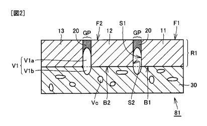
Referring to Figs. 1 and 2, a silicon carbide substrate 81 in accordance with
the
-6-
CA 02753373 2011-08-22 110214: 910353
present embodiment has a support portion 30 and a substrate region R1.
Substrate
region RI has single crystal substrates 11 to 19 and spaces (space portions)
GP. Space
portion GP has a filled portion 20. Substrate region R1 and support portion 30
have a
void VI bridging the interface therebetween. Specifically, void VI has a void
V l a
included in substrate region RI and a void Vlb included in support portion 30.
Void
VI is positioned at the border between each of single crystal substrates 11 to
19 when
viewed two-dimensionally. Further, support portion 30 has voids Vc therein.
Single crystal substrate 11 (first single crystal substrate) has a first front-
side
surface F1 and a first backside surface B 1 opposite to each other, and a
first side surface
S 1 connecting the first front-side surface F 1 and the first backside surface
B 1. Single
crystal substrate 12 (second single crystal substrate) has a second front-side
surface F2
and a second backside surface B2 opposite to each other, and a second side
surface S2
connecting the second front-side surface F2 and the second backside surface
B2. The
first and second single crystal substrates are arranged such that the first
and second side
surfaces Si and S2 face each other with a space GP therebetween. The shortest
distance between the first and second side surfaces is preferably at most 5
mm, more
preferably at most 1 mm, further preferably at most 100 m, and most
preferably at
most 10 m.
The front-side surface of each of single crystal substrates 11 to 19
preferably has
the plane orientation of {03-38}. It is noted, however, that {0001 }, { 1 1-
20} or { 1-
100} may be used as the plane orientation. Further, a plane off from each of
the
above-mentioned plane orientation by a few degrees may also be used.
Filled portion 20 fills a part of space GP to connect the first and second
front-
side surfaces F 1 and F2. Since space GP has relatively large void V 1 a as
shown in Fig.
2, it has, higher porosity (second porosity) as compared with the porosity
(first porosity)
of each of single crystal substrates 11 to 19.
Support portion 30 is joined to each of single crystal substrates 11 to 19,
for
example, to each of the first and second backside surfaces B 1 and B2. Support
portion
-7-
CA 02753373 2011-08-22 110214:910353
30 has, for example, a disk-shape, of which diameter is preferably at least 50
mm, and
more preferably, at least 150 mm.
The number of voids per unit volume is larger in support portion 30 than in
each
of single crystal substrates 11 to 19. Preferably, the number of voids per
unit volume
in support portion 30 is at least 10cm 3. Here, the number of voids refers to
the
number of voids having a certain volume or larger, and the volume is, for
example, 1 m3.
Further, the dislocation density of each of single crystal substrates 11 to 19
is
lower than the dislocation density of support portion 30. Specifically,
crystal quality is
higher in single crystal substrates 11 to 19 than in support portion 30.
Preferably, each of single crystal substrates 11 to 19 has a first
concentration as
impurity concentration per unit volume, and support portion 30 has a second
concentration as the impurity concentration per unit volume. The second
concentration is higher than the first concentration.
Next, the method of manufacturing silicon carbide substrate 81 will be
described.
For simplicity of description, in the following, only the single crystal
substrates 11 and
12 may be referred to among single crystal substrates 11 to 19. It is noted,
however,
that single crystal substrates 13 to 19 are processed in the same manner as
single crystal
substrates 11 and 12.
Referring to Figs. 3 and 4, support portion 30, single crystal substrates 11
to 19,
that is, a group 10 of single crystal substrates, and a heating apparatus are
prepared.
The heating apparatus has first and second heating bodies 91 and 92, a heat-
insulating
container 40, a heater 50, and a heater power source 150. Heat-insulating
container 40
is formed of a material having high heat-insulation property. Heater 50 is,
for example,
an electric resistance heater. The first and second heating bodies 91 and 92
absorb
radiant heat from heater 50 and re-radiate the heat, to attain the function of
heating
support portion 30 and the group 10 of single crystal substrates. First and
second
heating bodies 91 and 92 are formed, for example, of graphite having low
porosity.
Thereafter, first heating body 91, the group 10 of single crystal substrates,
-8-
CA 02753373 2011-08-22 110214:910353
support portion 30 and second heating body 92 are arranged stacked in this
order.
Specifically, first, single crystal substrates 11 to 19 are arranged in a
matrix on first
heating body 91. By way of example, single crystal substrates 11 and 12 are
arranged
such that the first and second side surfaces Si and S2 face each other with a
space GP
therebetween. Then, on the surfaces of group 10 of single crystal substrates,
support
portion 30 is placed. Thereafter, on support portion 30, second heating body
92 is
placed. Thereafter, the first heating body, the group 10 of single crystal
substrates,
support portion 30 and the second heating body 92 stacked one after another
are housed
in heat-insulating container 40 provided with heater 50.
Next, the atmosphere in heat-insulating container 40 is set to a reduced
pressure
atmosphere. Pressure of the atmosphere is set to be higher than 10-'Pa and
lower than
104 Pa.
The atmosphere described above may be an inert gas atmosphere. As the inert
gas, rare gas such as He or Ar, nitrogen gas, or a mixed gas of rare gas and
nitrogen gas
may be used. When the mixed gas is used, the ratio of nitrogen gas is, for
example,
60%. The pressure in heat-insulating container 40 is preferably at most 50kPa,
and
more preferably at most lOkPa.
Thereafter, by heater 50, the group 10 of single crystal substrates and
support
portion 30 are heated to a temperature that causes sublimation and re-
crystallization
reaction, through first and second heating bodies 91 and 92. Heating is done
to
produce temperature difference such that the temperature of support portion 30
becomes higher than the temperature of group 10 of single crystal substrates.
Referring to Fig. 5, at the start of heating mentioned above, support portion
30
is simply placed on each of single crystal substrates 11 and 12 and not joined
thereto.
Therefore, between each of the backside surfaces (upper surfaces in Fig. 5) of
single
crystal substrates 11 and 12 and support portion 30, there are small gaps GQ.
Further,
between single crystal substrates 11 and 12, a space GP is formed, as
described above.
Particularly, if the backside surfaces of single crystal substrates 11 and 12
are formed by
-9-
CA 02753373 2011-08-22 110214:910353
slicing, that is, formed by slicing and not subjected to polishing, there are
ups and downs
on the backside surfaces. Accordingly, by the spaces in concave portions of
ups and
downs, gaps of appropriate size can easily and reliably be provided.
When the temperature of support portion 30 is made higher than that of each of
single crystal substrates 11 and 12 as described above, material movement
occurs
because of sublimation, in gap GQ as indicated by an arrow Mc. Further,
material
movement occurs because of sublimation from support portion 30 to space GP, as
indicated by an arrow Mb. Further, material movement occurs because of
sublimation
in space GP as indicated by an arrow Ma, from the side of backside surface
(upper side
in the figure) to the side of front-side surface (lower side in the figure) of
each of single
crystal substrates 11 and 12.
Further, referring to Fig. 6, the material movement indicated by arrows Ma to
Mc in Fig. 5 correspond to cavity movement of cavities in space GP and gap GQ,
indicated by arrows Hla to Hlc in Fig. 6. Here, the height of gap GQ
(dimension in
the vertical direction in the figure) varies significantly in the plane, and
because of the
variation, velocity of cavity movement (arrow Hlc in the figure) corresponding
to gap
GP varies significantly in the plane.
Further, referring to Fig. 7, because of the variation, the cavity
corresponding to
gap GQ (Fig. 6) cannot move with its shape retained, and instead, a plurality
of voids Vc
(Fig. 7) are generated.
Further, by the movement of cavity corresponding to space GP indicated by
arrows Hla and Hlb (Fig. 6), filled portion 20 filling a part of space GP is
formed to
connect first and second front-side surfaces Fl and F2. As a result, void V1
consisting
of void V lb in support portion 30 facing space GP (Fig. 7) and void V 1 a
positioned in
space GP (Fig. 7) is generated.
As the heating continues, voids V 1 a, V 1 b and Vc move as indicated by
arrows
H2a, H2b and H2c, respectively. Thus, silicon carbide substrate 81 shown in
Fig. 2 is
obtained.
-10-
CA 02753373 2011-08-22 110214:910353
According to the present embodiment, since the dislocation density of each of
single crystal substrates 11 to 19 is lower than the dislocation density of
support portion
30, crystal quality of silicon carbide substrate can be made particularly
higher in each of
single crystal substrates 11 to 19. Further, since stress in silicon carbide
substrate is
alleviated by voids V1 and Vc, warpage of silicon carbide substrate 81 can be
reduced.
Further, the number of voids per unit volume is larger in support portion 30
than
in each of single crystal substrates 11 to 19. Therefore, it is possible to
surely provide
sufficiently large number of voids to alleviate stress by increasing the
number of voids in
support portion 30 while holding down the number of voids in each of single
crystal
substrates 11 to 19. Thus, warpage of silicon carbide substrate 81 can be
reduced
without degrading the quality of single crystal substrates 11 to 19.
Further, since first and second front-side surfaces F 1 and F2 (Fig. 2) are
formed,
the surface area of silicon carbide substrate 81 can be made larger than when
only the
first front-side surface F 1 is formed.
Further, space GP has filled portion 20 partially filling space GP to connect
the
first and second front-side surfaces F1 and F2. Thus, deposition of foreign
matter in
space GP can be prevented.
Further, since the porosity of space GP (second porosity) is higher than the
porosity of single crystal substrate 11 (first porosity), filled portion 20 is
more
susceptible to deformation. This means that stress can more easily be
alleviated by
filled portion 20 and, hence, warpage of silicon carbide substrate 81 can
further be
reduced. Preferably, the porosity of space GP is made larger than the porosity
of each
of other single crystal substrates 12 to 19.
Preferably, single crystal substrate 11 has a first concentration as impurity
concentration per unit volume, and support portion 30 has a second
concentration as the
impurity concentration per unit volume. The second concentration is higher
than the
first concentration. Thus, electric resistance of support portion 30 can be
made lower.
Preferably, the number of voids per unit volume in support portion 30 is at
least
-11-
CA 02753373 2011-08-22 110214:910353
10cm 3. Thus, warpage of silicon carbide substrate 81 can further be reduced.
Preferably, the number of voids mentioned above represents the number of voids
having the volume of at least 1 m3. Thus, warpage of silicon carbide substrate
81 can
further be reduced.
Preferably, each of single crystal substrates 11 to 19 has the SiC crystal
structure
of 4H polytype. Hence, silicon carbide substrate 81 suitable for the
manufacture of
power semiconductor can be obtained.
Preferably, in order to prevent cracking of silicon carbide substrate 81,
difference
in coefficient of thermal expansion between support portion 30 and single
crystal
substrates 11 to 19 is made as small as possible in silicon carbide substrate
81. Thus,
warpage of silicon carbide substrate 81 can further be reduced. For this
purpose,
support portion 30 may be adapted, for example, to have the same crystal
structure as
that of single crystal substrates 11 to 19.
Preferably, in-plane variation of thickness of support portion 30 and each of
the
group 10 of single crystal substrates (Fig. 4) prepared before heat treatment
is made as
small as possible. By way of example, the variation is limited to at most 10
m.
Electric resistance of support portion 30 prepared before heat treatment is
set
preferably lower than 50 mf2=cm and more preferably lower than l OmQ=cm.
The impurity concentration of support portion 30 of silicon carbide substrate
81
is preferably set to at least 5 x 10'8cm"3, and more preferably at least 1 x
1020cm-3.
When a vertical semiconductor device in which current is caused to flow in the
vertical
direction such as a vertical MOSFET (Metal Oxide Field Effect Transistor) is
manufactured using silicon carbide substrate 81 as such, on-resistance of the
vertical
semiconductor device can be reduced.
The average electric resistance of silicon carbide substrate 81 is preferably
at
most 5mS2=cm, and more preferably, at most lmf2=cm.
Preferably, the thickness of silicon carbide substrate 81 (dimension in the
vertical
direction in Fig. 2) is at least 300 m.
- 12-
CA 02753373 2011-08-22 110214: 910353
Preferably, the first front-side surface Fl has an off angle of at least 50
and at
most 65 with respect to the {0001 } plane. Consequently, channel mobility at
the first
front-side surface F 1 can be improved than when the first front-side surface
is the
{0001 } plane. More preferably, either the first or second condition below is
satisfied.
Under the first condition, an angle formed by the off orientation of first
front-
side surface F1 and the <1-100> direction of single crystal substrate 11 is at
most 5 .
More preferably, the off angle of first front-side surface F1 with respect to
the f03-38)
plane in the <1-100> direction of single crystal substrate 11 is at least -3
and at most 5 .
Under the second condition, an angle formed by the off orientation of first
front-
side surface Fl and the <11-20> direction of single crystal substrate 11 is at
most 5 .
Though the preferable orientation of first front-side surface F 1 of single
crystal
substrate 11 has been described in the foregoing, the same applies to the
surface
orientation of each of the remaining single crystal substrates 12 to 19.
(Embodiment 2)
Mainly referring to Fig. 8, different from Embodiment 1 (Fig. 2), a silicon
carbide substrate 82 in accordance with the present embodiment does not have
void Vlb
(Fig. 2). Silicon carbide substrate 82 can be obtained by forming filled
portion 20
mainly through material movement indicated by the arrow Ma (Fig. 5),
substantially
without material movement indicated by the arrow Mb (Fig. 5).
Except for this point, the structure is substantially the same as that of
Embodiment 1 described above. Therefore, the same or corresponding elements
are
denoted by the same reference characters and description thereof will not be
repeated.
The present embodiment also attains effects similar to those attained by
Embodiment 1.
(Embodiment 3)
Mainly referring to Fig. 9, a silicon carbide substrate 83 in accordance with
the
present embodiment has a substrate region R3 in place of substrate region R1
(Fig. 2).
Substrate region R3 has spaces GP fully filled with filled portions 21.
Further, support
portion 30 has voids V2 in addition to voids Vc. Voids V2 are positioned only
in the
-13-
CA 02753373 2011-08-22 110214: 910353
inside of support portion 30. Silicon carbide substrate 83 can be obtained by
continuing the heat treatment until voids V 1 enter and are fully positioned
in support
portion 30.
The material of filled portion 21 may include, for example, silicon carbide
(SiC),
silicon (Si), adhesive, resist, resin or silicon oxide (SiO2).
Except for this point, the structure is substantially the same as that of
Embodiment 1 described above. Therefore, the same or corresponding elements
are
denoted by the same reference characters and description thereof will not be
repeated.
The present embodiment also attains effects similar to those attained by
Embodiment 1.
(Embodiment 4)
Referring to Fig. 10, a silicon carbide substrate 84 in accordance with the
present
embodiment has a substrate region R4 in place of substrate region R1 (Fig. 2).
Substrate region R4 has unfilled space portions GP. In silicon carbide
substrate 84,
support portion 30 can be formed by depositing silicon carbide on the first
and second
backside surfaces B 1 and B2, for example, as indicated by the central arrow
in the figure.
Voids Vc are formed at the time of this deposition. Support portion 30 formed
by the
deposition may not necessarily have the single crystal structure, and it may
have
polycrystalline structure.
A modification of the present embodiment will be described with reference to
Fig.
11. In the present embodiment, support portion 30 having voids Vc is prepared
in
advance. As support portion 30, one similar to that of Embodiment 1 or a
polycrystalline body or a sintered body may be used. As indicated by the
arrows in the
figure, a surface of support portion 30 and backside surface of each of single
crystal
substrates 11 to 13 are joined. This joining may be done by heating the
interface
between each of single crystal substrates 11 to 13 and support portion 30.
Except for this point, the structure is substantially the same as that of
Embodiment 1 described above. Therefore, the same or corresponding elements
are
denoted by the same reference characters and description thereof will not be
repeated.
-14-
CA 02753373 2011-08-22 110214-910353)
The present embodiment also attains effects similar to those attained by
Embodiment 1.
(Embodiment 5)
Referring to Fig. 12, a silicon carbide substrate 85 in accordance with the
present
embodiment has a substrate region R5 in place of substrate region RI (Fig. 2).
Substrate region R5 has only the single crystal substrate 11, rather than
single crystal
substrates 11 to 19 (Fig. 1).
Except for this point, the structure is substantially the same as that of
Embodiment 1 described above. Therefore, the same or corresponding elements
are
denoted by the same reference characters and description thereof will not be
repeated.
The present embodiment also attains effects similar to those attained by
Embodiment 1.
(Embodiment 6)
Referring to Fig. 13, a silicon carbide substrate 86 in accordance with the
present
embodiment has a substrate region R6 in place of substrate region R5 (Fig.
12).
Substrate region R6 has a single crystal substrate 41 (third single crystal
substrate) in
addition to single crystal substrate 11. The third single crystal substrate 41
is joined to
the first front-side surface F 1 of single crystal substrate 11 (first single
crystal substrate).
Thus, substrate region R6 has a stacked structure.
(Seventh Embodiment)
Referring to Fig. 14, a semiconductor device 100 in accordance with the
present
embodiment is a vertical DiMOSFET (Double Implanted Metal Oxide Semiconductor
Field Effect Transistor), having silicon carbide substrate 81, a buffer layer
121, a
breakdown voltage holding layer 122, a p-region 123, an n+ region 124, a p+
region 125,
an oxide film 126, a source electrode 111, an upper source electrode 127, a
gate
electrode 110 and a drain electrode 112.
In the present embodiment, silicon carbide substrate 81 has n-type
conductivity
and, as described in Embodiment 1, it has support portion 30 and single
crystal substrate
11. Drain electrode 112 is provided on support portion 30 such that support
portion
is positioned between the drain electrode and single crystal substrate 11.
Buffer
- 15 -
CA 02753373 2011-08-22 110214.910353
layer 121 is provided on single crystal substrate 11 such that single crystal
substrate 11
is positioned between the buffer layer and support portion 30.
Buffer layer 121 has n-type conductivity, and its thickness is, for example,
0.5
m. The concentration of n-type conductive impurity in buffer layer 121 is, for
example, 5 x 1017cm 3.
Breakdown voltage holding layer 122 is formed on buffer layer 121, and it is
formed of silicon carbide having n-type conductivity. The thickness of
breakdown
voltage holding layer 122 is 10 m, and the concentration of n-type conductive
impurity
is 5 x 101503
On a surface of breakdown voltage holding layer 122, a plurality of p-regions
123 having p-type conductivity are formed spaced apart from each other. In p-
region
123, an n+ region 124 is formed at a surface layer of p-region 123. A p+
region 125 is
formed at a position next to n+ region 124. Extending from above n+ region 124
on
one p-region 123 over breakdown voltage holding layer 122 exposed between two
p-
regions 123, the other p-region 123 and above n+ region 124 in the said the
other p-
region 123, oxide film 126 is formed. On oxide film 126, gate electrode 110 is
formed.
Further, on n+ region 124 and p+ region 125, source electrode 111 is formed.
On
source electrode 111, an upper source electrode 127 is formed.
In a region within 10 nm from the interface between oxide film 126 and each of
the semiconductor layers, that is, n+ region 124, p+ region 125, p-region 123,
and
breakdown voltage holding layer 122, the highest concentration of nitrogen
atoms is at
least 1 x 1021cm 3. Therefore, mobility particularly at the channel region
below oxide
film 126 (the portion of p-region 123 in contact with oxide film 126 between
n+ region
124 and breakdown voltage holding layer 122) can be improved.
Next, the method of manufacturing semiconductor device 100 will be described.
Though process steps only in the vicinity of single crystal substrate 11 among
single
crystal substrates 11 to 19 (Fig. 1) are shown in Figs. 16 to 19, similar
process steps are
performed in the vicinity of each of single crystal substrates 12 to 19.
- 16-
CA 02753373 2011-08-22 110214:910353
First, at the substrate preparation step (step S 110: Fig. 15), silicon
carbide
substrate 81 (Figs. I and 2) is prepared. Silicon carbide substrate 81 has n-
type
conductivity.
Referring to Fig. 16, at the epitaxial layer forming step (step S 120: Fig.
15),
buffer layer 121 and breakdown voltage holding layer 122 are formed in the
following
manner.
First, on a surface of single crystal substrate 11 of silicon carbide
substrate 81,
buffer layer 121 is formed. Buffer layer 121 is formed on silicon carbide
having n-type
conductivity and, by way of example, it is an epitaxial layer of 0.5 .im in
thickness.
Further, concentration of conductive impurity in buffer layer 121 is, for
example, 5 x
1017cm 3.
Next, breakdown voltage holding layer 122 is formed on buffer layer 121.
Specifically, a layer formed of silicon carbide having n-type conductivity is
formed by
epitaxial growth. The thickness of breakdown voltage holding layer 122 is, for
example, 10 m. Concentration of n-type conductive impurity in breakdown
voltage
holding layer 122 is, for example, 5 x 10"cm".
Referring to Fig. 17, at the implantation step (step S 130: Fig. 15), p-region
123,
n+ region 124 and n+ region 125 are formed in the following manner.
First, p-type impurity is selectively introduced to a part of breakdown
voltage
holding layer 122, so that p-region 123 is formed. Next, n-type conductive
impurity is
selectively introduced to a prescribed region to form n+ region 124, and p-
type
conductive impurity is selectively introduced to a prescribed region to form
p+ region
125. Selective introduction of impurities is done using a mask formed, for
example, of
an oxide film.
Following the implantation step as such, an activation annealing treatment is
done. By way of example, annealing is done in an argon atmosphere, at a
heating
temperature of 1700 C for 30 minutes.
Referring to Fig. 18, the gate insulating film forming step (step S 140: Fig.
15) is
- 17 -
CA 02753373 2011-08-22 110214:910353
performed. Specifically, oxide film 126 is formed to cover breakdown voltage
holding
layer 122, p-region 123, n+ region 124 and p+ region 125. The film may be
formed by
dry oxidation (thermal oxidation). Conditions for dry oxidation are, for
example,
heating temperature of 1200 C and heating time of 30 minutes.
Thereafter, the nitrogen annealing step (step S 150) is done. Specifically,
annealing is done in a nitrogen monoxide (NO) atmosphere. Conditions for this
process are, for example, heating temperature of 1100 C and heating time of
120
minutes. As a result, nitrogen atoms are introduced to the vicinity of
interface between
each of breakdown voltage holding layer 122, p-region 123, n+ region 124 and
p+ region
125 and oxide film 126.
Following the annealing step using nitrogen monoxide, annealing using argon
(Ar) gas as an inert gas may be performed. Conditions for the process are, for
example,
heating temperature of 1100 C and heating time of 60 minutes.
Referring to Fig. 19, by the electrode forming step (step S 160: Fig. 15),
source
electrode 111 and drain electrode 112 are formed in the following manner.
First, on oxide film 126, using photolithography, a resist film having a
pattern is
formed. Using the resist film as a mask, portions of oxide film 126 positioned
on n+
region 124 and p+ region 125 are removed by etching. Thus, openings are formed
in
oxide film 126. Next, a conductive film is formed to be in contact with each
of n+
region 124 and p+ region 125 in the openings. Then, the resist film is
removed,
whereby portions of the conductive film that have been positioned on the
resist film are
removed (lift off). The conductive film may be a metal film and, by way of
example, it
is formed of nickel (Ni). As a result of this lift off, source electrode 111
is formed.
Here, heat treatment for alloying is preferably carried out. By way of
example,
heat treatment is done in an atmosphere of argon (Ar) gas as an inert gas, at
a heating
temperature of 950 C for 2 minutes.
Again referring to Fig. 14, on source electrode 111, upper source electrode
127
is formed. Further, on the backside surface of silicon carbide substrate 81,
drain
-18-
CA 02753373 2011-08-22 110214: 910353
electrode 112 is formed. On oxide film 126, gate electrode 110 is formed. By
the
above-described steps, semiconductor device 100 is obtained.
It is noted that a structure having conductivity types reversed from the
present
embodiment, that is, p-type and n-type reversed, may be used.
Further, the silicon carbide substrate for fabricating semiconductor device
100 is
not limited to silicon carbide substrate 81 in accordance with Embodiment 1,
and it may
be any of silicon carbide substrates 82 to 86 (Embodiments 2 to 6).
Further, though a vertical DiMOSFET has been described as an example, other
semiconductor devices may be manufactured using the semiconductor substrate in
accordance with the present invention. For instance, a RESURF-JFET (Reduced
Surface Field-Junction Field Effect Transistor) or a Schottky diode may be
manufactured.
EXAMPLES
As support portion 30 (Fig. 3), a silicon carbide wafer having the diameter of
100mm, thickness of 300 m, polytype 4H, plane orientation of (03-38), n-type
impurity
concentration of 1 x 1020cm 3, micropipe density of 1 x 104cm 2 and stacking
fault
density of 1 x 1015cm 1 was prepared. As each of the group 10 of single
crystal
substrates, that is, each of single crystal substrates 11 to 19 (Fig. 1), a
silicon carbide
wafer having the square shape of 20 x 20 mm, thickness of 300 m, polytype 4H,
plane
orientation of (03-38), n-type impurity concentration of 1 x 1019cm 3,
micropipe density
of 0.2cm 2 and stacking fault density smaller than 1 cm -1 was prepared.
Further, as
each of the first and second heating bodies 91 and 92, a graphite piece was
prepared.
Single crystal substrates 11 to 19 were arranged in a matrix on the first
heating
body 91. On the group 10 of single crystal substrates, support portion 30 was
placed.
Then, the second heating body 92 was placed on support portion 30. In this
manner, a
stacked body consisting of first heating body 91, group 10 of single crystal
substrates,
support portion 30 and second heating body 92 was prepared.
The stacked body described above was housed in heat-insulating container 40
-19-
CA 02753373 2011-08-22 110214-910353
(Fig. 3) of the heating apparatus. Next, the atmosphere in heat-insulating
container 40
was set to nitrogen atmosphere of 1Pa pressure. Thereafter, the temperature in
heat-
insulating container 40 was heated to about 2100 C by heater 50. Here, heating
was
done by heater 50 positioned closer to the second heating body 92 than the
first heating
body 9l . Asa result, the temperature of second heating body 92 was made
higher than
the first heating body 91. Accordingly, the temperature of the group 10 of
single
crystal substrates facing the first heating body 91 was made lower than the
temperature
of support portion 30 facing the second heating body 92. This state was kept
for 24
hours, to attain heat treatment. As a result, silicon carbide substrate 81
(Figs. 1, 2) was
obtained.
The number of voids per unit volume of support portion 30 of silicon carbide
substrate 81 was IOcm' or higher. Further, impurity concentration in support
portion
30 was 5 x 1020cm 3. Specifically, the impurity concentration of support
portion 30
after heat treatment was made higher than the value 1 x 1020cm 3 before heat
treatment.
The reason for this is considered that support portion 30 took in nitrogen in
the
atmosphere described above.
A cross-section of silicon carbide substrate 81 was inspected by an SEM
(Scanning Electron Microscope), and it was found that gaps GQ (Fig. 5) that
had
existed at the interface between single crystal substrate 11 and support
portion 30 before
heat treatment were substantially eliminated.
In the present example, the temperature of single crystal substrate 11 was
made
lower than the temperature of support portion 30 in the heat treatment, while
an
experiment of heat treatment without such temperature difference was
conducted. As
a result, it was found that more gaps GQ were left as compared with the
example of the
invention.
As further samples of the inventive example, silicon carbide substrates having
the
diameters of 50 mm, 75 mm, 100 mm, 125 mm and 150 mm were fabricated for each
of
plane orientations (0001) and (03-38), by the same method as described above.
As
-20-
CA 02753373 2011-08-22 110214:910353
comparative examples, substrates formed of single crystal corresponding to the
dimensions mentioned above were prepared. Each of these substrates was
subjected to
ion implantation and activation annealing. Conditions for activation annealing
were:
atmosphere was Ar atmosphere; pressure was 90 kPa; heat increase rate was
100 C/min; temperature was 1800 C; and holding time was 30 minutes.
Warpage of each of the substrates obtained in the above-described manner was
measured. The results were as shown in Table 1.
[Table 1]
Warpage m)
50 mm 75 mm 100 mm 125 mm 150 mm
Comparative (0001) <40 <50 <100 <200 <500
Examples (03-38) <30 <50 <70 <140 <300
Inventive (0001) <20 <30 <40 <50 <70
Examples (03-38) <20 <20 <30 <40 <50
The results indicated that warpage of substrates could be reduced in the
samples
of the invention.
Further, probability of cracking of each of the substrates was measured. The
results were as shown in Table 2.
[Table 2]
Probability of Cr king
50 mm 75 mm 100 mm 125 mm 150 mm
Comparative (0001) 1/10 1/10 3/10 4/10 7/10
Examples (03-38) 0/10 2/10 2/10 4/10 6/10
Inventive (0001) 0/10 0/10 0/10 0/10 0/10
Examples (03-38) 0/10 0/10 0/10 0/10 0/10
The results indicated that probability of cracking could be reduced in the
samples
of the invention.
Though Ar atmosphere was used for activation annealing in the examples above,
similar results were observed when other inert gas atmosphere such as He or N2
gas
atmosphere was used.
-21-
CA 02753373 2011-08-22 110214-910353
Correlation between the number of voids per unit volume in support portion 30
of silicon carbide substrate 81 and the warpage of substrate was studied. It
was found
that the smaller the number of voids per unit volume, the larger became the
warpage of
substrate. Further, it was found that crack was sometimes observed when the
number
of voids having the volume of 1 m3 or larger per unit volume was smaller than
10cm,3.
The embodiments as have been described here are mere examples and should not
be interpreted as restrictive. The scope of the present invention is
determined by each
of the claims with appropriate consideration of the written description of the
embodiments and embraces modifications within the meaning of, and equivalent
to, the
languages in the claims.
DESCRIPTION OF THE REFERENCE SIGNS
11 single crystal substrate (first single crystal substrate), 12 single
crystal
substrate (second single crystal substrate), 13-19 single crystal substrates,
20 filled
portion, 30 support portion, 41 single crystal substrate (third single crystal
substrate),
81-86 silicon carbide substrates, 91 first heating body, 92 second heating
body, 100
semiconductor device, Rl, R3-R6 substrate regions.
-22-